Integration of self-assembled discotic-based fibres into field-effect transistors: a comparison of preparation approaches†
Rebecca C.
Savage
a,
Jeffrey M.
Mativetsky
a,
Emanuele
Orgiu
a,
Matteo
Palma
a,
Gabin
Gbabode
b,
Yves H.
Geerts
b and
P.
Samorì
*b
aInstitut de Science et d'Ingénierie Supramoléculaires (ISIS)—CNRS 7006, Université de Strasbourg, 8 allée Gaspard Monge, 67000, Strasbourg, France. E-mail: samori@isis-ulp.org
bService de Chimie des Polymères, CP 206/01, Universités Libre de Bruxelles, Boulevard du Triomphe, 1050, Brussels, Belgium
First published on 18th October 2010
Abstract
The role played by the preparation method upon the morphological and electrical properties of alkyl substituted thio-triphenylene-based self-assembled fibres is explored by comparing two processing approaches, termed solvent vapour annealing (SVA) and solvent induced precipitation (SIP). Both approaches led to fibres having widths of several hundred nanometres and lengths of tens of micrometres. SVA formed isolated fibres which were tens of nanometres high, flat, and tapered at the ends. Conversely, SIP fibres exhibited nearly matching heights and widths, but organized into bundles. Despite these morphological differences, the same intermolecular packing is found by XRD in each type of structure, albeit with differing degrees of long-range order. The fibres were integrated into bottom-gate bottom-contact field-effect transistors. The density and configuration of the fibres with respect to the electrodes and gate dielectric were found to play an important role in the transport properties. SIP devices yielded the highest mobilities compared to SVA and spin-coated devices, largely owing to their high degree of internal order and the possibility to achieve high fibre densities within the transistor channel.
Introduction
There is great interest in using nanoscale self-assembled architectures of conjugated molecules as electroactive components in organic electronic devices.1–4 By using non-covalent intermolecular interactions to steer the assembly of materials, a high degree of molecular order can be achieved, resulting in improved electrical transport characteristics.5,6 Moreover, owing to the overall weak interactions governing the self-assembly, such systems have an intrinsic capacity, under mild processing conditions, to undergo repair of defects and grain boundaries which may otherwise act as bottlenecks for charge transport.7–10Polycyclic aromatic hydrocarbons in particular exhibit a marked propensity to stack into columnar architectures featuring a delocalization of the π-orbitals, thus enabling long range charge transport.11,12Alkyl chains are often substituted at the periphery of the molecules in order to increase the solubility in organic solvents and render the material easily processable for large-area applications. Such organic semiconductors are typically processed from solution onto surfaces by means of drop-casting, spin-coating or printing. However, these approaches suffer from secondary processes which are detrimental to long-range molecular ordering. For instance, spin-coating is characterized by fast solvent evaporation leading to kinetically driven assembly. Drop-casting features a slower drying process, subsequently yielding larger and more crystalline deposits; but, the long-range order is strongly influenced by shear forces which arise as the drop recedes during solvent evaporation.
In recent years two promising alternatives for producing self-assembled structures have been proposed which do not suffer from these drawbacks, these being solvent vapour annealing (SVA, Fig. 1a)13–21 and solvent or temperature induced precipitation (SIP, Fig. 1b, or TIP).6,13,21–27 During SVA a spin-coated or drop-cast film is exposed to a solvent vapour which condenses and forms a thin solvent layer at the sample surface, thus permitting the molecules to reorganize. This method has been successfully exploited to form n-type perylene nanowires,13–16,21 p-type pentacene6 and hexa-peri-hexabenzacoronene (HBC)15 fibres, ambipolar perylene/HBC dyad-based mesoscopic ribbons,19 and to improve the characteristics of organic field-effect transistors (OFETs).17–19 During SIP or TIP, molecules are induced to aggregate and precipitate from solution by modifying the chemical environment, e.g. by the addition of a non-solvent or through a decrease in temperature. This method has also been applied to perylene,13,22–26pentacene6,23,24 and HBC-derivatives27 and has been shown to be useful for the formation of self-assembled fibres for use in organic field-effect transistors (OFET)6,26,27 and complementary inverters.25,28
 | ||
| Fig. 1 (a) During Solvent Vapour Annealing (SVA) a previously spin-coated or drop-cast film is exposed to a solvent saturated atmosphere to enable molecular reorganization on the surface. (b) Solvent Induced Precipitation (SIP) causes fibres to precipitate in solution, either by adding a small amount of solution to a vial containing a non-solvent, or by multiple additions over several hours of a small amount of non-solvent to a vial containing the solution. | ||
Though SVA and SIP have been considered in separate studies, to the best of our knowledge, a systematic comparison of the two approaches, both in terms of the resulting fibre morphology and the efficacy for incorporating the fibres into OFET devices is lacking. To shed light on this we used a thioether-substituted triphenylene as a test system, a discotic molecule which has been observed to form highly structured liquid crystalline and crystalline phases by X-ray diffraction (XRD) studies.29–31 Previous charge transport studies have shown p-type behaviour,30,32–34 and an intracolumnar mobility up to 0.4 cm2 V−1s−1.35 Here we investigate the relationship between the morphology and the electrical characteristics of self-assembled fibres of 2,3,6,7,10,11 hexadecylthiotriphenylene (HDTT) prepared by spin-coating, SVA and two different types of SIP. The effect of the processing procedure on the morphology and intermolecular structure was studied by optical and atomic force microscopy (AFM), as well as X-ray diffraction (XRD), whereas the electrical properties were investigated by integrating the fibres into OFETs and measuring the transistor characteristics.
Experimental
The 2,3,6,7,10,11-hexadecylthiotriphenylene (HDTT) molecule (Fig. 2) was synthesized as reported previously.36 Purity was assessed by 1H-NMR spectroscopy and thin layer chromatography. No side-products were observed. The preparation of the fibres required the use of a solvent and non-solvent. For all experiments n-hexane (>99%, Carlo Erba) was used as a solvent and ethanol (98%, Fluka) as a non-solvent. All initial solutions were prepared to a concentration of 1 mM. Films were spin-coated onto pre-patterned electrodes (details below) from 50 µl solution at 800 rpm for 120 seconds. Devices prepared using SVA were similarly spin-coated, then enclosed in a hexane-saturated atmosphere for 36–48 h at room temperature (Fig. 1a).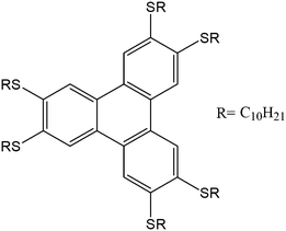 | ||
| Fig. 2 Chemical formula of 2,3,6,7,10,11 hexadecylthiotriphenylene (HDTT). | ||
When preparing fibres by SIP the rate of precipitation was modulated using two procedures, termed fast and slow SIP. For fast SIP a small quantity of solution was rapidly injected into a larger volume of non-solvent (ratio 1![[thin space (1/6-em)]](https://www.rsc.org/images/entities/char_2009.gif) :5), whereas for slow SIP fibres a non-solvent was dribbled into a vial with twice the volume of solution (Fig. 1b) every two hours, until the volume was three times that of the original solution. The vials containing the SIP precipitate were then left overnight to allow clustering, after which they could be picked up with a pipette and deposited onto pre-patterned electrodes, which were subsequently annealed to 45 °C on a laboratory hotplate before electrical characterization. Spin-coating, SVA treatment and deposition of the SIP fibres were performed inside a glovebox with H2O and O2 content below 1 ppm.
:5), whereas for slow SIP fibres a non-solvent was dribbled into a vial with twice the volume of solution (Fig. 1b) every two hours, until the volume was three times that of the original solution. The vials containing the SIP precipitate were then left overnight to allow clustering, after which they could be picked up with a pipette and deposited onto pre-patterned electrodes, which were subsequently annealed to 45 °C on a laboratory hotplate before electrical characterization. Spin-coating, SVA treatment and deposition of the SIP fibres were performed inside a glovebox with H2O and O2 content below 1 ppm.
Topographic AFM images were recorded under ambient conditions using a Digital Instruments Dimension 3100 AFM operating with a Nanoscope IV controller in tapping (intermittent-contact) mode, using commercial silicon cantilevers (Veeco MPP-11120) with a nominal spring constant of 40 N m−1, a resonance frequency of 300 kHz and a tip radius of 10 nm. The widths of structures were measured from the full width half maximum (FWHM) of the edges. No correction was made to account for tip broadening.
X-Ray diffraction measurements (XRDs) were performed on a Bruker D8 Advance diffractometer using Cu-Kα radiation (λ = 1.5418 Å), using samples prepared on bare SiOx substrates. Diffraction patterns were collected in the scattered angular range between 1.6° and 40° with an angular resolution of 0.02° per step and a typical counting time of 10 s per step, using θ/θ reflection geometry, i.e. with the sample holder fixed while the source and detector together move continuously on each side forming the same angle θ with its surface. X-Ray diffraction patterns are represented as the scattering intensity versus 2θ (in degrees), the angle between incident and diffracted X-ray beams.
Electrical characterization was performed in a glovebox with a N2 atmosphere, using a Cascade Microtech M150 probe station. Two electrometres, a Keithley 6517A and 2535, interfaced by in-house developed software (based on NI LabView) were used to source voltages and collect data. The FET substrates of Si/SiOx with pre-patterned electrodes were purchased from the Fraunhofer Institute for Photonic Microsystems. They were provided with highly doped Si as a gate (n ≈ 3 × 1017 cm−3), and a 230 nm layer of thermal SiOx as a dielectric. The interdigitated electrodes consisted of 30 nm of Au on a 10 nm ITO adhesion layer (completely covered by the gold), and had channel lengths (L) of 2.5, 5, 10 and 20 µm, and a width (W) of 10 mm (i.e.W/L = 4000, 2000, 1000 and 500).
Results and discussion
Morphology
AFM-measurements of spin-coated films on SiOx surfaces revealed a network of interconnected domains with a lateral size of a few hundred nanometres and a thickness of 4 ± 1 nm (Fig. 3a). When these films were exposed to a solvent (hexane) saturated atmosphere during SVA, they re-arranged to form anisotropic linear structures, attaining lengths of up to 30 µm, heights of 20 ± 10 nm and widths of 400 ± 100 nm. The fibres typically tapered down to widths of 100 nm or less towards the ends (Fig. 3b). The upper surfaces of the fibres had a roughness under one nanometre (Fig. S1a†). The formation of the fibres can be ascribed to the tendency of HDTT molecules to self-associate via π−π stacking29,31 of the aromatic cores, facilitated during SVA by a thin film of condensed solvent which forms on the substrate.20 Similar structures were formed on Au surfaces (see on top of electrodes in Fig. 6c and d). It was also observed that fibres preferred to nucleate along topographical features (Fig. 6c and d).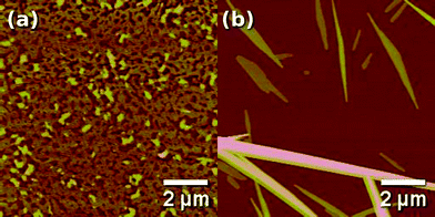 | ||
| Fig. 3 Topographical AFM images of an HDTT spin-coated film on SiOx (a) as prepared and (b) after SVA treatment. z-Scale: (a) 50 nm and (b) 150 nm. | ||
By combining a solution of HDTT in hexane with the non-solvent ethanol, the molecules were induced to aggregate into mesoscopic fibres. The speed of mixing the liquids determines the dynamics of the self-assembly, thus by modulating the time of preparation the dimensions of the fibres could be tuned.26 To determine the role that the precipitation rate plays in the self-assembly we compared two distinct protocols, termed fast- and slow-SIP (Fig. 1b). Fig. 4 shows the morphology of HDTT fibres prepared by fast (Fig. 4a and b) and slow SIP (Fig. 4c and d). The size of the two types of fibres was noticeably different, the fast SIP fibres being considerably smaller, having widths of 340 ± 150 nm, heights of 280 ± 140 nm (as seen by AFM, Fig. 4a) and lengths of 25 ± 3 µm (as measured by optical microscopy, Fig. 4b). The slow SIP fibres on the other hand were 1000 ± 200 nm wide, 500 ± 200 nm tall and 200 ± 60 µm long (Fig. 4c and d). Interestingly, no significant variation in either the widths or heights of the SIP fibres was observed over tens of microns. Unlike the SVA fibres, which formed on a surface and were significantly wider than they were tall, the SIP fibres formed in an isotropic medium and displayed comparable widths and heights as might be expected. The fact that they exhibit in all samples a greater width than height can be largely accounted for by tip broadening. The well-defined, straight edges suggest a considerable long-range order within the fibres. Moreover, the tops of both types of SIP fibres frequently had steps of tens of nanometres in height running parallel to the axis of the structures (Fig. S1b†). SIP fibres typically formed bundles, with the individual fibres lying parallel or twining around each other with a random helicity and pitch. This was particularly evident in the case of fast SIP (Fig. 4a). On a larger scale, optical microscopy showed that multiple bundles of fibres were often attached together at one end, apparently from a common nucleation site.
 | ||
| Fig. 4 The fibres produced by fast and slow SIP showed some notable differences, the most obvious being their different sizes: fast SIP fibres, seen in (a) AFM and (b) optical microscopy, were considerably shorter than slow SIP fibres, as seen in (c) AFM and (d) optical microscopy. All samples prepared on SiOx, vertical scale of (a) is 1000 nm and (c) 1500 nm. | ||
Crystallographic structure
The XRD patterns of the spin-coated films before and after SVA are similar and both consist in a set of equally spaced reflections which are at the same positions for the two samples (see Table 1 and Fig. S2†). The first reflection at low angle corresponds to a repeating intermolecular distance of 2.74 nm while the other ones at higher angles are the higher orders of this reflection (from 2 to 6), indicating a long range intercolumnar stacking order perpendicularly to the surface. Interestingly only these reflections are observed, indicating a preferential orientation of the family of reticular planes responsible for these diffraction peaks parallel to the substrate surface.37 As HDTT molecules are known to pack into columnar assemblies29,38,39 this intermolecular distance of 2.74 nm is likely to correspond to an intercolumnar distance. This means that for both samples the columnar axis is preferentially oriented parallel to the substrate surface in a planar alignment. The crystalline order along this intercolumnar direction has been quantified for the two samples from the width of the first diffraction peak, by means of the correlation length L (Table 1) calculated using the Scherrer equation.40 This value corresponds to the distance over which the repeating distance between planes in a family of reticular planes is kept coherent, or in other words the length over which the order is maintained along a particular crystallographic direction. A slight improvement of the crystalline order along the substrate normal was evident after SVA treatment, hence it was found that the correlation length increased from 18 nm for the spin-coated film to 32 nm for the SVA-treated samples. This, when taking into account the uncertainties of these values of around 10 nm, is in agreement with the heights determined by AFM on the same samples. This does not, however, provide information about the structural coherence along the axis of the fibres which, based on the anisotropic structure shown by AFM, is expected to be significantly longer.| Order | Film dobs/nm | SVA dobs/nm | Fast SIPdobs/nm | Slow SIPdobs/nm |
|---|---|---|---|---|
| 1 | 2.74 | 2.74 | 2.74 | 2.74 |
| 2 | 1.39 | 1.38 | 1.38 | 1.37 |
| 3 | 0.91 | 0.92 | 0.92 | 0.92 |
| 4 | 0.68 | 0.69 | 0.69 | 0.69 |
| 5 | 0.55 | 0.55 | 0.55 | 0.55 |
| 6 | 0.46 | 0.46 | 0.46 | 0.46 |
| 7 | — | — | 0.39 | — |
| Correlation length/nm | 18 | 32 | 74 | 150 |
The XRD patterns of fast and slow SIP samples are superimposed in Fig. 5. Correlated peaks (up to 7th order for fast SIP samples) corresponding to an intermolecular distance of 2.74 nm are, again, observed for both samples (Table 1), demonstrating that the same overall structural arrangement is exhibited by all HDTT samples whatever the crystallization process undertaken (be it spin-coated films, SVA and SIP treatments). Crystalline order is enhanced from fast SIP to slow SIP treatment, which can be seen by the sharpening of the 1st order intercolumnar reflection (inset in Fig. 5). The correlation length increases from 74 nm to 150 nm (Table 1) which can be linked to the increase of the fibres’ lateral dimensions from fast SIP to slow SIP samples pointed out by AFM. The unit cell dimensions could be determined for the solid phase using the XRD pattern of slow SIP sample which presents several sharp reflections up to 22° in 2θ (Fig. 5). Because the intercolumnar distances were found to be the same for all sample types analyzed, it is considered highly unlikely that this distance could be maintained with a different structural arrangement, therefore it is inferred that all sample types have the same molecular packing. The unit cell was determined to be monoclinic (a = 2.775 ± 0.5 nm, b = 0.448 ± 0.1 nm, c = 2.741 ± 0.1 nm, and β = 90.63 ± 7°) with space groupP21 and 2 molecules in the unit cell (complete crystallographic data and peak indexations are given in ESI, Table S1†). The unit cell is similar to that of non-substituted triphenylene, whose crystal structure has been determined from single crystals,38 and which is orthorhombic with space groupP212121. The a and c parametres (which correspond to the a and b parametres in the crystal structure of triphenylene) are much larger due to the presence of the six alkylthiol chains. The columnar axis is parallel to b, this being the shortest axis and perpendicular to the (a, c) plane. The much larger value of b compared to the typical π–π distance (around 0.35 nm) indicates that HDTT molecules are titled towards the columnar axis by an angle α ≈ 40° (α = a cos (b/3.5)). The intense reflections observed between 0.285 nm and 0.260 nm for fast SIP sample can be indexed using the already determined cell parameters. They correspond to hkl reflections with k ≠ 0 (see ESI), indicating that the corresponding reticular planes are related to the intracolumnar arrangement of molecules (all peaks observed at 2θ < 19° are h0l reflections, then corresponding to intercolumnar distances). Then, the observation of these reflections for fast SIP samples could indicate the presence of small domains with homeotropic-like alignment of columns, i.e. columnar axis perpendicular to the substrate. In the present case, we hypothesize that the columns lean from the substrate normal with an angle equal to α so that the HDTT molecules lie flat on the substrate surface. Indeed, the normal to each family of reticular planes corresponding to the reflections observed between 0.285 and 0.260 nm, makes an angle of about 50° with the columnar axis (calculated from the cell parameters and the hkl indexations of the reflections concerned), which is then nearly parallel to the normal to the plane of the HDTT molecules. The diffraction of these reticular planes would then be observed with a “flat-on” orientation of HDTT molecules towards the substrate surface, in other words with the columnar axis bent from the substrate normal. We assume that the presence of domains with homeotropic-like alignment of HDTT columns in fast SIP samples originates from a fast crystallization process during the aggregation procedure. It is thought that, in addition to the predominant alignment along the fibre axis, there is also a stacking of HDTT molecules frozen in at the solid state along various orientations.
 | ||
| Fig. 5 XRD patterns measured at 30 °C for the fast SIP and slow SIP samples. Numbers above the diffraction peaks indicate the order of the correlated reflections. Inset is a zoom on the first order reflection (peak intensity has been multiplied by 3 in the case of the slow SIP in a sake of comparison). | ||
Preparation of FET devices
When preparing transistor devices from self-assembled fibres three important parameters are the coverage of the electrode gap, and the nature of both the fibre–electrode and fibre–dielectric interface. The devices made from SIP fibres were fabricated by depositing fibres onto electrodes. Once the solvent had evaporated the procedure could be repeated until a layer covering most of the devices had been formed (Fig. 6). Based on optical microscope measurements, the transistor channels for the fast SIP devices were estimated to be 80 to 90% covered (Fig. 6a) while the slow SIP devices were 60 to 90% covered (Fig. 6b). It should be noted that though the overall coverage of the devices could be further enhanced by depositing more material, this would not necessarily increase the quantity of material contributing to the electrical transport since it is known that the greatest contribution to charge transport in FETs comes from the first few nanometres of electroactive material at the interface between semiconductor and dielectric layer.41,42 | ||
| Fig. 6 Optical microscopy images of fibres prepared by (a) fast SIP and (b) slow SIP. (c and d) Topographical AFM of SVA prepared fibres, with z-scale (c) 90 nm, and (d) 150 nm. All samples prepared on pre-patterned Au electrodes on SiOx. | ||
Unlike the SIP fibres, which were formed in a vial and then deposited on the substrate, the SVA fibres assembled directly on the Au electrodes and SiOx surface. It was observed that the fibres formed on both materials, despite the different balance between solvent–surface and molecule–surface interactions. Due to preferential nucleation at the electrode edges the fibres were often found to bridge the electrode gaps (Fig. 6c), though this was not always the case (Fig. 6d). Due to this the smaller 2.5 µm gaps were 60 to 90% filled with material, whereas the larger gaps only had 30 to 40% coverage. Again, it should be noted that especially for the larger gaps, significant amounts of the material present in the channel did not actively contribute to the charge transport as it did not bridge the entire channel length (Fig. 6d). This sparse coverage of the device can be understood on the basis of the fibre formation process during SVA, for though the fibres form from homogeneous films, during SVA treatment the molecules rearrange into more condensed structures leading to the depletion of large areas of the device.
Another important aspect is the physical contact of the fibres with the electrodes and the underlying dielectric. It is expected, especially for the case of shorter fibres, that they do not span the entire gap, or that fibres may bridge the gap but not make contact with the electrode (e.g. in the case of SIP they may remain suspended above, supported by other fibres). This leads to difficulties in making an accurate estimation of the true active area of the device, thus hindering a precise quantification of the charge carrier mobility, which is inversely related to the channel width (W) through
 | (1) |
Transistor properties
The electrical properties of the three different types of molecular fibres (SVA, fast SIP, and slow SIP) and spin-coated films were explored by fabricating FET devices with pre-patterned Au source and drain electrodes in a bottom-gate, bottom-contact configuration and gap lengths of 2.5, 5, 10 and 20 µm. The transfer and output characteristics from a fast SIP device are displayed in Fig. 7. The transfer curve in the saturation regime shows a clear gate dependence of the drain current, with low values in the sub-threshold region and Ion/Ioff in the order of 105. However, a noticeable contact resistance can be deduced by looking at the output curves (Fig. 7, inset) where the substantial flattening at low drain voltages can be ascribed to poor charge injection. The complex phenomenon of the charge injection from the electrodes to the fibre can be modelled as an extra resistive component in series with the transistor channel.44 In particular, an injection barrier (Φp) for holes between the HOMO level of the semiconductor and the gold work function (ΦM,Au) of the electrodes can arise when the former is higher in (negative) energy than the latter, leading to difficulties of charge injection from the electrode into the semiconductor. In our study, the work function of gold was measured in argon environment by Macroscopic Kelvin and found to be 5.12 eV with a standard deviation lower than 0.02 eV. Compared to the HOMO level of a molecule with the same core as ours which is reportedly around −5.3 eV,45 an injection barrier Φp from the gold to the HDTT fibres must be then taken into account. The presence of such a barrier can be invoked to partially explain the above-mentioned curve flattening observed on the linear region of the transistor output curves. Further, it has been pointed out that also the morphology at the metal–organic interface plays an important role for the injection properties.46,47 As a result of all these factors, the drain current is very low until a certain drain voltage is reached (approximately −10 V), and the output curves are shifted to the right along the voltage axis. All mobilities were extracted from the transfer curves in the linear regime using eqn (1). Threshold voltages (VT) were calculated from the intersection with the x-axis of the calculated fit to the linear part of the transfer characteristics.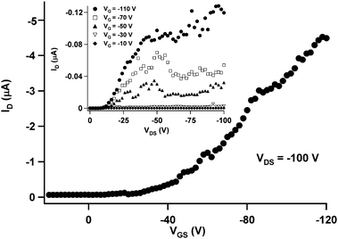 | ||
| Fig. 7 Transfer characteristics of a fast-SIP device with a 2.5 µm channel length in the saturation regime. Inset shows output characteristics of the same device. | ||
The mobilities of fast SIP devices were found to decrease with increased channel length (Fig. 8). This effect was not observed in the slow SIP devices, i.e. those with longer fibres, for those devices with channel lengths below 20 µm. Since the fast SIP fibres had lengths comparable to the two longer electrode gap sizes (10 and 20 µm), and the fibres were randomly oriented on the surface, it is expected that the transport in these cases took place predominantly through overlapping fibres. The subsequent decrease in mobility highlights the detrimental role of inter-fibre junctions on the overall performance.11 This effect would be considerably less pronounced in the case of the longer, slow SIP fibres, which could easily cross the electrode gaps even at an oblique angle.
 | ||
| Fig. 8 Average device mobilities of the SIP- and SVA-prepared devices. | ||
Table 2 presents the average mobilities of at least six 2.5 µm devices, found to be (3 ± 0.4) × 10−6 cm2 V−1s−1 for the fast SIP, and (2 ± 0.5) × 10−7 cm2 V−1s−1 for the slow SIP, with the best fast SIP devices attaining values of up to 2 × 10⁻⁵ cm2 V−1s−1. The mobilities of spin-coated films and SVA-treated devices were independent of channel length, with average mobilities of (5 ± 4) × 10−7 and (6 ± 4) × 10−8 cm2 V−1 s−1 respectively (averaged over at least three devices). As mentioned previously, these values do not take into account the incomplete coverage of the devices, thus overestimating the effective channel width W and underestimating the mobility. The significant decrease in device performance following SVA treatment of films would potentially be reduced if the coincident decrease in coverage were taken into account. However, when preparing devices using SVA, though the surface is initially covered with material, during exposure to solvent vapours molecular rearrangement depletes large areas of the surface. Consequently, though SVA has been seen to form highly ordered structures it is inevitable accompanied by a significant decrease of coverage, something which must be taken into account when using the SVA technique.
Nevertheless, even with these factors taken into account, the mobilities are orders of magnitude below the theoretically predicted value of 1 cm2 V−1s−1 for transport along the main columnar axis of triphenylene stacks.32,33 Still, it must be noted that this can only be considered a theoretical upper limit, as reported experimental values in similar systems for single-domains are an order of magnitude lower, at 0.4 cm2 V−1s−1, as measured by pulse-radiolysis time-resolved microwave conductivity (PR-TRMC).35 Moreover, in actual OFET devices, one must also take into account the effect of grain boundaries and interfacial trapping, both which are expected to severely affect charge transport, and thus further decrease mobility values.11,30,32,34 However, with proper understanding of the various preparation techniques, procedures and device geometry can be optimized to overcome these bottlenecks, allowing device performances to approach the inherent transport properties of supramolecular π–π architectures.
The observed threshold voltages were remarkably high, with average values of −50 ± 3, −50 ± 10, −90 ± 30 and −100 ± 20 V for films, SVA, fast and slow SIP respectively (Table 2). The threshold voltage of the devices is affected by the nature of the electrode–fibre and dielectric–fibre interfaces.48 The fact that the largest VT values were measured for SIP devices suggests that these fibres formed a poorer contact to the electrodes. This is likely to stem from the reduced interaction of the SIP fibres with the electrodes and the gate dielectric, as discussed in the Preparation of FET devices section. That the SIP devices also display a considerably wider range of threshold voltages highlights the variability of the detailed device structure.
Conclusions
We have characterized the morphology of SIP and SVA-based supramolecular thio-triphenylene fibres, and compared their electrical characteristics in an OFET configuration with that of untreated films. The dimensions of fibres prepared by SIP could be tuned by modulating the precipitation dynamics during the preparation, thus forming fibres from tens to hundreds of microns in length. SVA treatment of a spin-coated film was also seen to form highly anisotropic structures, typically tapering towards the ends. Despite these morphological differences the molecular packing arrangement was found to be the same, irrespective of the preparation method, consisting of columnar assemblies running parallel to the substrate. The X-ray structure of the SVA-treated sample showed more crystallinity than the spin-coated film. So too did the fast- and slow-SIP fibres, the latter in particular exhibiting sharper diffraction peaks than all the other samples, thereby indicating the greatest degree of long-range order. The fast SIP also showed evidence for additional reticular planes of molecules, probably frozen in during the fast crystallization process. The fact, however, that this does not reflect on the transport properties of the related devices leads to the conclusion that it is not merely the greatest degree of internal order that gives rise to the best devices, but that also the integration of the structures into the device is critical. This was also seen when comparing SIP with SVA devices, for though SVA devices exhibited lower threshold voltages, due to the poor spanning of the electrode channel the average mobilities of these devices were lower. A further consequence of morphology upon device characteristics was that the mobility of the fast SIP devices scaled inversely to the channel length due to the comparable fibre and channel length for the larger channels. In the view of improving future devices, it would be interesting to explore methods to prepare more homogeneous and aligned layers of fibres. Several methods have been reported, such as aligning pre-prepared fibres using soft lithographic embossing49 or a filtration and transfer method (FAT),26 or alternatively inducing directional growth by taking advantage of dewetting effects50–53 or applying electric54–57or magnetic-fields.11,58 In conclusion, we think that when using alignment in conjunction with appropriate surface treatment59 self-assembled supramolecular fibres are very promising for future large-scale production of organic electronics.Acknowledgements
This work was supported by the EC through the FP7 ONE-P large-scale project no. 212311 and the Marie Curie ITN-SUPERIOR (PITN-GA-2009-238177), the NanoSci-E+ project SENSORS and the International Center for Frontier Research in Chemistry (FRC).Notes and references
- J. S. Wu, W. Pisula and K. Müllen, Chem. Rev., 2007, 107, 718–747 CrossRef CAS.
- A. R. Murphy and J. M. J. Fréchet, Chem. Rev., 2007, 107, 1066–1096 CrossRef CAS.
- A. P. H. J. Schenning and E. W. Meijer, Chem. Commun., 2005, 3245–3258 RSC.
- S. Sergeyev, W. Pisula and Y. H. Geerts, Chem. Soc. Rev., 2007, 36, 1902–1929 RSC.
- C. D. Dimitrakopoulos and P. R. L. Malenfant, Adv. Mater., 2002, 14, 99–117 CrossRef CAS.
- D. H. Kim, D. Y. Lee, H. S. Lee, W. H. Lee, Y. H. Kim, J. I. Han and K. Cho, Adv. Mater., 2007, 19, 678–682 CrossRef CAS.
- R. Dabirian, V. Palermo, A. Liscio, E. Schwartz, M. B. J. Otten, C. E. Finlayson, E. Treossi, R. H. Friend, G. Calestani, K. Müllen, R. J. M. Nolte, A. E. Rowan and P. Samorì, J. Am. Chem. Soc., 2009, 131, 7055–7063 CrossRef CAS.
- K. Puntambekar, J. P. Dong, G. Haugstad and C. D. Frisbie, Adv. Funct. Mater., 2006, 16, 879–884 CrossRef CAS.
- J. Zhang, J. P. Rabe and N. Koch, Adv. Mater., 2007, 20, 3254–3257.
- P. Annibale, C. Albonetti, P. Stoliar and F. Biscarini, J. Phys. Chem. A, 2007, 111, 12854–12858 CrossRef CAS.
- I. O. Shklyarevskiy, P. Jonkheijm, N. Stutzmann, D. Wasserberg, H. J. Wondergem, P. C. M. Christianen, A. Schenning, D. M. de Leeuw, Z. Tomovic, J. S. Wu, K. Müllen and J. C. Maan, J. Am. Chem. Soc., 2005, 127, 16233–16237 CrossRef CAS.
- X. L. Feng, V. Marcon, W. Pisula, M. R. Hansen, J. Kirkpatrick, F. Grozema, D. Andrienko, K. Kremer and K. Müllen, Nat. Mater., 2009, 8, 421–426 CrossRef CAS.
- K. Balakrishnan, A. Datar, T. Naddo, J. Huang, R. Oitker, M. Yen, J. Zhao and L. Zang, J. Am. Chem. Soc., 2006, 128, 7390–7398 CrossRef CAS.
- A. Datar, R. Oitker and L. Zang, Chem. Commun., 2006, 1649–1651 RSC.
- G. De Luca, A. Liscio, F. Nolde, L. M. Scolaro, V. Palermo, K. Müllen and P. Samorì, Soft Matter, 2008, 4, 2064–2070 RSC.
- G. De Luca, A. A. Liscio, P. P. Maccagnani, F. Nolde, V. Palermo, K. Müllen and P. Samorì, Adv. Funct. Mater., 2007, 17, 3791–3798 CrossRef CAS.
- K. C. Dickey, J. E. Anthony and Y. L. Loo, Adv. Mater., 2006, 18, 1721–1726 CrossRef CAS.
- W. H. Lee, D. H. Kim, J. H. Cho, Y. Jang, J. A. Lim, D. Kwak and K. Choa, Appl. Phys. Lett., 2007, 91, 092105 CrossRef.
- J. M. Mativetsky, M. Kastler, R. C. Savage, D. Gentilini, M. Palma, W. Pisula, K. Müllen and P. Samorì, Adv. Funct. Mater., 2009, 19, 2486–2494 CrossRef CAS.
- E. Treossi, A. Liscio, X. Feng, V. Palermo, K. Müllen and a. P. Samorı, Small, 2009, 5, 112–119 CrossRef CAS.
- A. Datar, K. Balakrishnan, X. Yang, X. Zuo, J. Huang, R. Oitker, M. Yen, J. Zhao, D. M. Tiede and L. Zang, J. Phys. Chem., 2006, 110, 12327–12332 Search PubMed.
- K. Balakrishnan, A. Datar, R. Oitker, H. Chen, J. Zuo and L. Zang, J. Am. Chem. Soc., 2005, 127, 10496–10497 CrossRef CAS.
- A. L. Briseno, S. C. B. Mannsfeld, S. A. Jenekhe, Z. Bao and Y. Xia, Mater. Today, 2008, 11, 38–47 CrossRef CAS.
- A. L. Briseno, S. C. B. Mannsfeld, X. Lu, Y. Xiong, S. A. Jenekhe, Z. Bao and Y. Xia, Nano Lett., 2007, 7, 668–675 CrossRef CAS.
- A. L. Briseno, S. C. B. Mannsfeld, C. Reese, J. M. Hancock, Y. Xiong, S. A. Jenekhe, Z. Bao and Y. Xia, Nano Lett., 2007, 7, 2847–2853 CrossRef CAS.
- J. H. Oh, H. W. Lee, S. Mannsfeld, R. M. Stoltenberg, E. Jung, Y. W. Jin, J. M. Kim, J. B. Yoo and Z. N. Bao, Proc. Natl. Acad. Sci. U. S. A., 2009, 106, 6065–6070 CAS.
- S. X. Xiao, J. Y. Tang, T. Beetz, X. F. Guo, N. Tremblay, T. Siegrist, Y. M. Zhu, M. Steigerwald and C. Nuckolls, J. Am. Chem. Soc., 2006, 128, 10700–10701 CrossRef CAS.
- M. M. Ling, Z. N. Bao, P. Erk, M. Koenemann and M. Gomez, Appl. Phys. Lett., 2007, 90, 3.
- E. F. Gramsbergen, H. J. Hoving, W. H. Dejeu, K. Praefcke and B. Kohne, Liq. Cryst., 1986, 1, 397–400 CrossRef CAS.
- D. Adam, P. Schuhmacher, J. Simmerer, L. Haussling, K. Siemensmeyer, K. H. Etzbachi, H. Ringsdorf and D. Haarer, Nature, 1994, 371, 141–143 CrossRef CAS.
- E. Fontes, P. A. Heiney and W. H. Dejeu, Phys. Rev. Lett., 1988, 61, 1202–1205 CrossRef CAS.
- J. Cornil, V. Lemaur, J. P. Calbert and J. L. Bredas, Adv. Mater., 2002, 14, 726–729 CrossRef CAS.
- V. Lemaur, D. A. Da Silva Filho, V. Coropceanu, M. Lehmann, Y. Geerts, J. Piris, M. G. Debije, A. M. Van de Craats, K. Senthilkumar, L. D. A. Siebbeles, J. M. Warman, J. L. Bredas and J. Cornil, J. Am. Chem. Soc., 2004, 126, 3271–3279 CrossRef CAS.
- J. M. Warman and P. G. Schouten, J. Phys. Chem., 1995, 99, 17181–17185 CrossRef CAS.
- A. M. van de Craats, J. M. Warman, M. P.d. Haas, D. Adam, J. Simmerer, D. Haarer and P. Schuhmacher, Adv. Mater., 1996, 8, 823–826 CrossRef CAS.
- O. Roussel, G. Kestemont, J. Tant, V. de Halleux, R. Gómez Aspe, J. Levin, A. Remacle, I. Raluca Gearba, D. Ivanov, M. Lehmann and Y. Geerts, Mol. Cryst. Liq. Cryst., 2003, 396, 35–39 CrossRef CAS.
- The D8 Advance diffractometer works in a reflection mode with a θ/θ geometry, thus, by this geometry, diffraction can only be obtained by molecular planes which have their normal parallel to that of the sample holder, i.e. parallel to the sample substrate.
- F. R. Ahmed and J. Trotter, Acta Crystallogr., 1963, 16, 503–508 CrossRef CAS.
- Y. Maeda, D. S. S. Rao, S. K. Prasad, S. Chandrasekhar and S. Kumar, Liq. Cryst., 2001, 28, 1679–1690 CrossRef CAS.
- L (Å) = Kl/(b cos q) where K is a constant (K = 0.9), λ is the wavelength of the X-ray radiation (1.5418 Å), β is the full width at half maximum of the peak expressed in 2θ (radians) and θ is the angular position of the peak (2θ/2).
- C. Tanase, E. J. Meijer, P. W. M. Blom and D. M. de Leeuw, Org. Electron., 2003, 4, 33–37 CrossRef CAS.
- F. Dinelli, M. Murgia, P. Levy, M. Cavallini, F. Biscarini and D. M. de Leeuw, Phys. Rev. Lett., 2004, 92, 116802 CrossRef.
- G. Horowitz, R. Hajlaoui, H. Bouchriha, R. Bourguiga and M. Hajlaoui, Adv. Mater., 1998, 10, 923–927 CrossRef CAS.
- P. Stallinga and H. L. Gomes, Synth. Met., 2006, 156, 1305–1315 CrossRef CAS.
- B. M. Zhao, B. Liu, R. Q. Png, K. Zhang, K. A. Lim, J. Luo, J. J. Shao, P. K. H. Ho, C. Y. Chi and J. S. Wu, Chem. Mater., 2010, 22, 435–449 CrossRef CAS.
- H. N. Tsao, W. Pisula, Z. H. Liu, W. Osikowicz, W. R. Salaneck and K. Müllen, Adv. Mater., 2008, 20, 2715–2719 CrossRef CAS.
- C. A. Liu, Z. H. Liu, H. T. Lemke, H. N. Tsao, R. C. G. Naber, Y. Li, K. Banger, K. Müllen, M. M. Nielsen and H. Sirringhaus, Chem. Mater., 2010, 22, 2120–2124 CrossRef CAS.
- M. Kitamura, Y. Kuzumoto, S. Aomori, M. Kamura, J. H. Na and Y. Arakawa, Appl. Phys. Lett., 2009, 94, 083310 CrossRef.
- A. M. Hung and S. I. Stupp, Nano Lett., 2007, 7, 1165–1171 CrossRef CAS.
- N. Liu, Y. Zhou, L. Wang, J. Peng, J. Wang, J. Pei and Y. Cao, Langmuir, 2009, 25, 665–671 CrossRef CAS.
- S. C. B. Mannsfeld, A. Sharei, S. H. Liu, M. E. Roberts, I. McCulloch, M. Heeney and Z. A. Bao, Adv. Mater., 2008, 20, 4044–4048 CrossRef CAS.
- V. Palermo and P. Samorì, Angew. Chem., Int. Ed., 2007, 46, 4428–4432 CrossRef CAS.
- R. van Hameren, P. Schon, A. M. van Buul, J. Hoogboom, S. V. Lazarenko, J. W. Gerritsen, H. Engelkamp, P. C. M. Christianen, H. A. Heus, J. C. Maan, T. Rasing, S. Speller, A. E. Rowan, J. A. A. W. Elemans and R. J. M. Nolte, Science, 2006, 314, 1433–1436 CrossRef CAS.
- M. Mas-Torrent, D. den Boer, M. Durkut, P. Hadley and A. P. H. J. Schenning, Nanotechnology, 2004, 15, S265–S269 CrossRef CAS.
- B. W. Messmore, J. F. Hulvat, E. D. Sone and S. I. Stupp, J. Am. Chem. Soc., 2004, 126, 14452–14458 CrossRef CAS.
- L. Sardone, V. Palermo, E. Devaux, D. Credgington, M. De Loos, G. Marletta, F. Cacialli, J. Van Esch and P. Samorì, Adv. Mater., 2006, 18, 1276–1280 CrossRef CAS.
- M. Yoshio, Y. Shoji, Y. Tochigi, Y. Nishikawa and T. Kato, J. Am. Chem. Soc., 2009, 131, 6763–6767 CrossRef CAS.
- D. Lowik, I. O. Shklyarevskiy, L. Ruizendaal, P. C. M. Christianen, J. C. Maan and J. C. M. van Hest, Adv. Mater., 2007, 19, 1191–1195 CrossRef.
- K. Suemori, S. Uemura, M. Yoshida, S. Hoshino, N. Takada, T. Kodzasa and T. Kamata, Appl. Phys. Lett., 2007, 91, 192112 CrossRef.
Footnote |
| † Electronic supplementary information (ESI) available: further experimental details. See DOI: 10.1039/c0jm01754j |
| This journal is © The Royal Society of Chemistry 2011 |