Assembly of shape-controlled nanocrystals by depletion attraction†‡
Marco
Zanella
,
Giovanni
Bertoni
,
Isabella R.
Franchini
,
Rosaria
Brescia
,
Dmitry
Baranov§
and
Liberato
Manna
*
Istituto Italiano di Tecnologia, Via Morego 30, 16163 Genova, Italy. E-mail: liberato.manna@iit.it
First published on 1st October 2010
Abstract
Recently (Baranov et al., Nano Lett., 2010, 10, 743) we demonstrated that depletion attraction between semiconductor nanorods in solution can be employed for both their self-assembly and their separation from spherical nanoparticles. Here we show that depletion attraction can be used to fabricate binary superlattices of nanorods and 3D networks of octapod/tetrapod-shaped nanocrystals.
The variety of nanocrystal sizes, shapes and compositions that is now possible to synthesize and the tunable properties that nanocrystals exhibit has triggered interest in their assembly, for applications in materials and devices.2 Progress has been made in organizing spherical nanocrystals in single, binary (including quasi-crystalline), quasi-ternary and ternary superlattices,3 and in assembling nanorods.4 Depletion attraction (DA) forces can also be involved in nanocrystal assembly.5 So far they have been exploited mainly in the areas of macromolecules and colloids. They have purely entropic origin and their contribution emerges in concentrated solutions of micro/nano-particles in presence of macromolecules like proteins or polymers. When two particles approach each other at a distance smaller than the diameter of the macromolecules, the latter are excluded from the volume between the particles. The formation of a region of pure solvent generates an osmotic pressure which pushes the particles together. The pressure scales according to the amount of excluded volume (to the macromolecules) between the two particles, which depends on the size and the shape of the particles involved. It was shown that DA can affect the formation of binary nanoparticle superlattices,6 it governs the “bundling” of TiO2 nanorods in the presence of oleic acid,7 it can be used to separate gold nanorods in mixtures with spheres,8 and regulates lock-and-key interactions in spherical colloids.9 We employed DA for in-solution assembly of CdSe(sphere, core)/CdS(rod, shell) nanorods and for their separation from spherical nanoparticles.1 Here we use DA for fabricating binary nanorod superlattices, for assembling branched nanocrystals in network structures and for shape-selective separation of other nanocrystals in addition to those reported so far, proving the power of DA in colloidal chemistry.
We fabricated various types of nanorod superlattices via DA. We report here two examples, one based on semiconductor CdSe rods and soft magnetic Fe2P rods, and one based on CdSe/CdS rods and Cu2Se/Cu2S rods. We first proved that the various rod samples could self-organize into ordered superlattices in solution in the presence of molecules like oleylamine or oleic acid. In the experiments, the molecules were added to a solution of rods until it became turbid, indicating the formation of assemblies.1,10 The solution was centrifuged and the precipitate rinsed several times with ethanol in order to remove the excess of additive, and then re-suspended in ethanol. A few drops of this solution were deposited on a carbon-coated TEM grid and the solvent was evaporated. Fig. 1 shows results for Fe2P nanorods, prepared as described in ref. 11 with 4.9 nm diameter and 15.5 nm length (on average) and coated with oleylamine and trioctylphosphine. On the grid we observed bundles of hexagonally packed nanorods, which were organized both in monolayers (Fig. 1a and b) and in multilayers (Fig. 1c and d).12 The main process involved in the formation of monolayers should be most likely nucleation and growth rather than spinodal decomposition, while multilayers should be formed by aggregation of the once formed monolayers, in analogy with results from recent calculations.12 At room temperature these rods are superparamagnetic, and do not have an intrinsic dipole moment (space group is P![[6 with combining macron]](https://www.rsc.org/images/entities/char_0036_0304.gif) 3m, which has a mirror plane perpendicular to the c-axis).11 Hence their organization in solution should be driven preferentially by DA.
3m, which has a mirror plane perpendicular to the c-axis).11 Hence their organization in solution should be driven preferentially by DA.
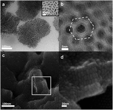 | ||
| Fig. 1 (a) Transmission electron microscope (TEM) image of monolayer bundles of vertically aligned Fe2P rods. Insets: TEM image of Fe2P rods before assembly; (b) high magnification view of a monolayer bundle highlighting hexagonal packing symmetry; (c) scanning electron microscope (SEM) image of multilayer bundles. A magnified SEM view of a multilayer structure of (c) (rotated by 90° clockwise) is displayed in (d). | ||
Binary superlattices (up to 1–2 μm in size) were prepared by applying the procedure described above to the mixture of Fe2P and CdSe nanorods in toluene (the latter prepared following ref. 13 with 5.8 nm diameter and 17.6 nm length, on average).
In order to distinguish between CdSe and Fe2P rods in the bundles (Fig. 2a), energy filtered transmission electron microscopy (EFTEM) was used (Fig. 2b). The two types of rods had comparable diameters and lengths, hence random 2D superstructures of hexagonally packed nanorods are expected in which the occupancy of each lattice site should be dictated by the relative ratio of the two components. In practice, some clustering of Fe2P nanorods could be found among the more abundant CdSe rods. The latter observation might be explained by differences in cumulative attractive force (with electrostatic, van der Waals and dipole–dipole interactions contributing) experienced by rods of different materials and with different capping ligands (oleylamine and trioctylphosphine for Fe2P, alkylphosphonates for CdSe). To minimize differences in size and surface chemistry we fabricated binary superlattices of nanorods of similar average dimensions (3.6 nm diameter, 28 nm length) and coated by the same surfactants (alkylphosphonates). To realize this, one fraction of a sample of CdSe/CdS nanorods (prepared following ref. 13) was exposed to Cu+ ions. This led to exchange of Cd2+ ions in the nanocrystal lattice with Cu+ ions.10 This procedure is similar to the one reported by Alivisatos et al. recently.14 The cation exchanged sample was then mixed with the fraction of pristine CdSe/CdS rods, and assembly was triggered as described above (Fig. 2c). As in the previous case, clustering of the less abundant Cu-based rods (0.4 molar ratio, according to elemental analysis) was observed (Fig. 2d, and ref. 10). There could be several reasons for this clustering, for example assembly might be also influenced by dipolar interactions, which are material-sensitive, or cation exchange modified the packing and/or density of surfactant molecules on the nanocrystal surface, hence influencing van der Waals interactions among them.
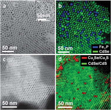 | ||
| Fig. 2 (a) Elastic-filtered image of a binary superlattice of Fe2P and CdSe nanorods; inset: TEM image of non-assembled CdSe nanorods; (b) false color image after superimposing the elemental map of Fe (from Fe L edge) with the Fe L pre-edge, the latter resembling the elemental map of Cd. (c) Elastic-filtered image of a binary superlattice of CdSe/CdS nanorods and Cu-exchanged CdSe/CdS nanorods; (d) false color image after superimposing the elemental map of Cd with that of Cu. | ||
We also exploited DA for assembling branched nanocrystals. Tetrapod-shaped nanocrystals do not exhibit any distinctive self-organized patterns on TEM grids if deposited by conventional techniques adapted from spherical nanocrystals experience. To the best of our knowledge there are no experimental reports of this kind, while a recent theoretical work described a “cubatic” liquid crystalline phase for tetrapod-shaped particles observed in simulations.15 We considered as test systems ZnTe(core)/CdTe(arms) tetrapods and CdSe(core)/CdS(arms) octapods, prepared following recipes developed by us.16 These particles were chosen because of their regular branching and monodispersity. To induce assembly, either oleic acid or a solution of PMMA or PEG-MA (Mw ≈ 15![[thin space (1/6-em)]](https://www.rsc.org/images/entities/char_2009.gif) 000 and Mn ≈ 526, respectively) in toluene was mixed with a concentrated solution of nanocrystals (either tetrapods or octapods) in toluene. For tetrapods, PMMA or PEG-MA was often chosen instead of oleic acid as the latter was found to etch CdTe over time. The assembly of tetrapods in 3D aggregates and 2D networks (Fig. 3) might be due to combined influence of DA forces and specific interactions between nanoparticles and additives (e.g. weak binding or particular bundling of macromolecules). Three different aggregation patterns were observed for tetrapods (Fig. 3). Fragments of treeing (Fig. 3a) and interlacing (Fig. 3c) tetrapods were formed by using either oleic acid or PEG-MA, while honeycomb-like 2D networks (Fig. 3b) were observed in high yield when PMMA was used.10 For octapods, mainly chain-like structures were seen, in addition to large aggregates (Fig. 4), and it was difficult to distinguish if they were due to treeing or to interlacing, due to the large number of arms present in each nanocrystal. In these chains the assembly of nanocrystals appears to maximize the amount of solvent excluded between them. Both types of branched nanoparticles were nicely aligned over short-ranges (up to 10–20 nanoparticles) but lacked long-range order. Further experimental studies and convergence with theoretical simulations will provide better understanding and control over assembly of colloids with complex shapes. We also found that shape selective precipitation by DA can be extended to a variety of materials. As a proof of principle, we report in the ESI‡ the selective precipitation of high aspect ratio TiO2 and WO3 nanorods (prepared as described in ref. 17 from shorter aspect ratio rods and spheres.
000 and Mn ≈ 526, respectively) in toluene was mixed with a concentrated solution of nanocrystals (either tetrapods or octapods) in toluene. For tetrapods, PMMA or PEG-MA was often chosen instead of oleic acid as the latter was found to etch CdTe over time. The assembly of tetrapods in 3D aggregates and 2D networks (Fig. 3) might be due to combined influence of DA forces and specific interactions between nanoparticles and additives (e.g. weak binding or particular bundling of macromolecules). Three different aggregation patterns were observed for tetrapods (Fig. 3). Fragments of treeing (Fig. 3a) and interlacing (Fig. 3c) tetrapods were formed by using either oleic acid or PEG-MA, while honeycomb-like 2D networks (Fig. 3b) were observed in high yield when PMMA was used.10 For octapods, mainly chain-like structures were seen, in addition to large aggregates (Fig. 4), and it was difficult to distinguish if they were due to treeing or to interlacing, due to the large number of arms present in each nanocrystal. In these chains the assembly of nanocrystals appears to maximize the amount of solvent excluded between them. Both types of branched nanoparticles were nicely aligned over short-ranges (up to 10–20 nanoparticles) but lacked long-range order. Further experimental studies and convergence with theoretical simulations will provide better understanding and control over assembly of colloids with complex shapes. We also found that shape selective precipitation by DA can be extended to a variety of materials. As a proof of principle, we report in the ESI‡ the selective precipitation of high aspect ratio TiO2 and WO3 nanorods (prepared as described in ref. 17 from shorter aspect ratio rods and spheres.
 | ||
| Fig. 3 Assemblies of ZnTe/CdTe tetrapods. Fragments of treeing (a) and interlacing (c) of tetrapods induced by PEG-MA and oleic acid respectively. Honeycomb-like networks of tetrapods (b) formed with PMMA present in solution. Models of the various assemblies are sketched in the bottom right panel. | ||
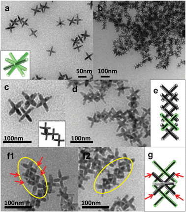 | ||
| Fig. 4 (a) TEM image of non-assembled CdSe/CdS octapods. Most octapods have a cross shape in transmission when four of their arms touch the carbon support film on the grid and they are aligned with the remaining four arms pointing away from the film. (b–d) and (f1, f2) TEM images of various assemblies induced by oleic acid. Models of the various assemblies are also sketched. | ||
In summary, we show how DA forces can be used to assemble nanorods and branched nanocrystals of different materials, and for shape selective precipitation. Superlattices of nanorods of similar size but different chemical composition could be used in various applications. For example, if the two materials have suitable band gaps and offsets, their superlattices could be exploited in photovoltaics. If one of the materials is magnetic, the whole superlattice could be manipulated and/or trapped viamagnetic tweezers. With branched nanoparticles high surface area, “porous” materials could be prepared, and if the polymer that induced DA is semiconducting, the network of interlaced nanocrystals and polymer could be of interest for photovoltaics.
This work was financially supported in part by the FP7 starting ERC grant NANO-ARCH (contract no. 240111). We acknowledge Angela Fiore, Rosanna Mastria and Karol Miszta, for help with nanocrystal synthesis, Alessandro Genovese and Sergio Marras for help with electron microscopy imaging.
Notes and references
- D. Baranov, A. Fiore, M. van Huis, C. Giannini, A. Falqui, U. Lafont, H. Zandbergen, M. Zanella, R. Cingolani and L. Manna, Nano Lett., 2010, 10, 743 CrossRef CAS.
- R. Q. Song and H. Colfen, Adv. Mater., 2010, 22, 1301 CrossRef CAS; D. V. Talapin, J. S. Lee, M. V. Kovalenko and E. V. Shevchenko, Chem. Rev., 2010, 110, 389 CrossRef CAS; R. Costi, A. E. Saunders and U. Banin, Angew. Chem., Int. Ed., 2010, 49, 4878 CrossRef CAS; N. A. Frey, S. Peng, K. Cheng and S. Sun, Chem. Soc. Rev., 2009, 38, 2532–2542 RSC; I. R. Franchini, A. Cola, A. Rizzo, R. Mastria, A. Persano, R. Krahne, A. Genovese, A. Falqui, D. Baranov, G. Gigli and L. Manna, Nanoscale, 2010 10.1039/c0nr00308e.
- H. Friedrich, C. J. Gommes, K. Overgaag, J. D. Meeldijk, W. H. Evers, B. de Nijs, M. P. Boneschanscher, P. E. de Jongh, A. J. Verkleij, K. P. de Jong, A. van Blaaderen and D. Vanmaekelbergh, Nano Lett., 2009, 9, 2719 CrossRef CAS; E. V. Shevchenko, D. V. Talapin, N. A. Kotov, S. O'Brien and C. B. Murray, Nature, 2006, 439, 55 CrossRef; E. V. Shevchenko, J. B. Kortright, D. V. Talapin, S. Aloni and A. P. Alivisatos, Adv. Mater., 2007, 19, 4183 CrossRef CAS; D. V. Talapin, E. V. Shevchenko, M. I. Bodnarchuk, X. C. Ye, J. Chen and C. B. Murray, Nature, 2009, 461, 964 CrossRef CAS; W. H. Evers, H. Friedrich, L. Filion, M. Dijkstra and D. Vanmaekelbergh, Angew. Chem., Int. Ed., 2009, 48, 9655 CAS.
- K. M. Ryan, A. Mastroianni, K. A. Stancil, H. T. Liu and A. P. Alivisatos, Nano Lett., 2006, 6, 1479 CrossRef CAS; S. Gupta, Q. Zhang, T. Emrick and T. P. Russell, Nano Lett., 2006, 6, 2066 CrossRef CAS; S. Ahmed and K. M. Ryan, Nano Lett., 2007, 7, 2480 CrossRef CAS; A. Guerrero-Martinez, J. Perez-Juste, E. Carbo-Argibay, G. Tardajos and L. M. Liz-Marzan, Angew. Chem., Int. Ed., 2009, 48, 9484 CrossRef CAS; J. L. Baker, A. Widmer-Cooper, M. F. Toney, P. L. Geissler and A. P. Alivisatos, Nano Lett., 2010, 10, 195 CrossRef CAS; X. L. Fang, Y. Li, C. Chen, Q. Kuang, X. Z. Gao, Z. X. Xie, S. Y. Xie, R. B. Huang and L. S. Zheng, Langmuir, 2010, 26, 2745 CrossRef CAS.
- S. Asakura and F. Oosawa, J. Chem. Phys., 1954, 22, 1255 CAS.
- D. K. Smith, B. Goodfellow, D. M. Smilgies and B. A. Korgel, J. Am. Chem. Soc., 2009, 131, 3281 CrossRef CAS.
- B. Ye, G. D. Qian, X. P. Fan and Z. Y. Wang, Curr. Nanosci., 2010, 6, 262 Search PubMed.
- K. Park, H. Koerner and R. A. Vaia, Nano Lett., 2010, 10, 1433 CrossRef CAS.
- S. Sacanna, W. T. M. Irvine, P. M. Chaikin and D. J. Pine, Nature, 2010, 464, 575 CrossRef CAS.
- See ESI‡ for details on materials and methods.
- J. P. Park, B. Koo, Y. Hwang, C. Bae, K. An, J. G. Park, H. M. Park and T. Hyeon, Angew. Chem., Int. Ed., 2004, 43, 2282 CrossRef CAS.
- A. Patti and M. Dijkstra, Phys. Rev. Lett., 2009, 102, 128301 CrossRef.
- L. Carbone, C. Nobile, M. De Giorgi, F. D. Sala, G. Morello, P. Pompa, M. Hytch, E. Snoeck, A. Fiore, I. R. Franchini, M. Nadasan, A. F. Silvestre, L. Chiodo, S. Kudera, R. Cingolani, R. Krahne and L. Manna, Nano Lett., 2007, 7, 2942 CrossRef CAS.
- P. K. Jain, L. Amirav, S. Aloni and A. P. Alivisatos, J. Am. Chem. Soc., 2010, 132, 9997 CrossRef CAS.
- R. Blaak, B. M. Mulder and D. Frenkel, J. Chem. Phys., 2004, 120, 5486 CrossRef CAS.
- A. Fiore, R. Mastria, M. G. Lupo, G. Lanzani, C. Giannini, E. Carlino, G. Morello, M. De Giorgi, Y. Li, R. Cingolani and L. Manna, J. Am. Chem. Soc., 2009, 131, 2274 CrossRef CAS; S. Deka, K. Miszta, D. Dorfs, A. Genovese, G. Bertoni and L. Manna, Nano Lett., 2010, 10, 3770 CrossRef CAS.
- J. W. Seo, Y. W. Jun, S. J. Ko and J. Cheon, J. Phys. Chem. B, 2005, 109, 5389 CrossRef CAS; R. Buonsanti, V. Grillo, E. Carlino, C. Giannini, T. Kipp, R. Cingolani and P. D. Cozzoli, J. Am. Chem. Soc., 2008, 130, 11223 CrossRef CAS.
Footnotes |
| † This article is part of the ‘Emerging Investigators’ themed issue for ChemComm. |
| ‡ Electronic supplementary information (ESI) available: Details on the syntheses and TEM; additional examples of superlattices; TEM images demonstrating shape selective precipitation. See DOI: 10.1039/c0cc02477e |
| § Present address: Department of Chemistry, University of Chicago, Chicago, IL 60637, USA. |
| This journal is © The Royal Society of Chemistry 2011 |