Si nanoparticle-decorated Si nanowire networks for Li-ion battery anodes†
Liangbing
Hu
,
Hui
Wu
,
Seung Sae
Hong
,
Lifeng
Cui
,
James R.
McDonough
,
Sy
Bohy
and
Yi
Cui
*
Department of Materials Science and Engineering, Stanford University, Stanford, California 94305, USA. E-mail: yicui@stanford.e
First published on 10th September 2010
Abstract
We designed and fabricated binder-free, 3D porous silicon nanostructures for Li-ion battery anodes, where Si nanoparticles electrically contact current collectors via vertically grown silicon nanowires. When compared with a Si nanowire anode, the areal capacity was increased by a factor of 4 without having to use long, high temperature steps under vacuum that vapour–liquid–solid Si nanowire growth entails.
Silicon is an attractive anode material for lithium ion batteries because of its highest known theoretical capacity (∼4200 mA h g−1). One major challenge for Si anodes is their large volume changes by up to 400% upon insertion and extraction of lithium. Previous studies on bulk Si and micrometre sized particles as electrodes in lithium ion batteries only lead to modest capacities, ∼800 mA h g−1, with rapid capacity fading.1,2 There are primarily two engineering methods for improving the cycling performance of Si as an anode material, which involve overcoming the mechanical difficulties associated with the large volume expansion upon lithiation. One is based on Si thin films, as they allow the anisotropic expansion of the material. Silicon thin films, sometimes on porous current collectors, show improved cycling performance. However, the film thickness is usually a few hundred nanometres, which leads to an areal capacity of ∼0.1 mA h cm−2 and is insufficient for viable applications.3,4 The other approach is based on Si nanostructures with enough porous volume to buffer the Si expansion. Electrodes based on silicon nanoparticles (NPs) with sizes ∼50–100 nm using slurry methods also show poor cycling.5 Recently, Cho et al. successfully demonstrated that agglomeration-free silicon NPs with sizes less than 20 nm lead to improved performance.6 Yushin et al. used a bottom-up approach for Si NPs to realize high-performance anodes with excellent stabilities and high rate capabilities.7Silicon nanowires (NWs) directly grown on stainless steel lead to 75% utilization of Si's maximum capacity with little fading during cycling.8 This is due to the one dimensional structure's ability to accommodate large strains without pulverization. Following that, a variety of forms of Si-based 1D nanostructures have also been developed, including a silicon coating on carbon fibers, silicon nanotubes, and silicon–carbon nanocomposites.9,10 These facile designs share a common attribute: the electrodes are highly porous and electrically connected to current collectors. During the Li insertion, the pores allow enough space for Si to expand to release the strain. However, one drawback of using Si NW electrodes grown by chemical vapour deposition (CVD) in our previous study is its relatively low mass loading, ∼0.3 mg cm−2. Longer growth times could increase the mass loading, which makes the cost prohibitively high. A silicon coating on carbon fibers or other conductive backbones could achieve large mass loadings, ∼1 mg cm−2, which requires approximately half an hour of Si deposition time.
In this work, we use vertically grown Si NWs on stainless steel as nanoporous substrates to deposit Si NPs based on an aqueous, binder-free Si NP ink. This design has several main advantages as a high energy density anode: first, the commercial silicon NPs, with diameters ∼50 nm, effectively increase the mass loading of Si NW electrodes. The low viscosity of the Si ink allows for good penetration of Si NPs in the Si NW network. Second, the Si NWs function as both active electrode materials and electrical pathways to current collectors for the Si NPs. The native oxide coatings on Si NPs and organics would impede the electrical contact. The organic surfactant will decompose at high temperature. If the insulating oxide between Si NPs and Si NWs prohibit charge transport, the chemical vapor deposition (CVD) Si overcoating can function as the conductive path for Si NPs to current collector. Third, the nanoporous 3D structure here provides enough space for the expansion of both Si NWs and NPs after Li insertion, resulting in a stable capacity during cycling. Through this design, we achieved a high mass loading of 1.5 mg cm−2 and a discharge capacity of 1600 mA h g−1 using a lower cutoff voltage of 0.05 V vs.Li/Li+. Minimal fading of capacity is observed after 50 cycles. When compared with Si NW anodes, we effectively increase the areal capacity by a factor of 4 without having to use long, high temperature steps under vacuum that vapour–liquid–solid (VLS) Si NW growth entails.
Fig. 1(a) shows the design of the binder-free structure, where Si NWs are grown by a CVD method through the VLS mechanism with mass loadings of ∼0.3 mg cm−2 and Si NPs are embedded in Si NWs to form a decorated network. Subsequently, a thin layer of Si by a CVD method overcoats the entire network to ensure the excellent electrical conduction between Si NPs and Si NWs, along with the stainless steel substrates. The details of Si NW growth by a CVD method can be found in our previous publications.8 For the Si NP deposition, an aqueous Si ink was prepared. Si NPs with sizes ∼50 nm were purchased from Sigma Aldrich. The Si NPs were dispersed in water with 1% by weight sodium dodecylbenzenesulfonate (SDBS) as a surfactant. The dispersion concentration was 10 mg mL−1 and the ink is stable for several months. Fig. 1(b) shows a photo of the yellowish dispersion. Fig. 1(c) shows its dynamic viscosity which is close to that of distilled water. The binder-free ink shows Newtonian-like fluidic behavior with low viscosity, which allows the ink to easily penetrate into the Si NW network once dropped on its surface. Due to the rough surfaces of the Si NW substrates, the aqueous ink is well anchored to the substrate which leads to a uniform coating. For comparison, we also tried to deposit Si NPs directly onto flat, bare stainless steel substrates. Due to the low viscosity, the aqueous ink moves around which results in poor uniformity. The binder-free, decorated networks on 1 cm by 1 cm stainless steel (SS) substrates are then overcoated by CVD with a thin silicon layer to ensure good electrical contact between Si NPs and silicon NWs, where silicon NWs function as electrical contacts to current collectors.10
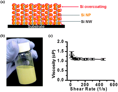 | ||
| Fig. 1 (a) Scheme of a network of Si NP-decorated Si NWs. The Si NPs are drop casted directly onto CVD-grown Si NW networks on SS substrates to increase the mass loading of active materials. Si NW networks provide rough surfaces for Si NPs to stick to. A Si overcoating was used to electrically “glue” Si nanoparticles to NWs. (b) Aqueous, 10 mg mL−1Si ink with 1% SDBS as surfactant. (c) Viscosity vs. shear rate of aqueous Si ink. | ||
The morphology of the Si NW network and the decorated network is shown in Fig. 2. As shown in Fig. 2(a) and (b), the Si NW network has large spaces for filling in Si NPs. The Si NWs are vertically grown from the substrate, with lengths up to 10 μm. The areal mass density is 0.3 mg cm−2, which varies with the VLS time and catalyst density. SEM confirms the successful deposition of Si NPs onto Si NW networks. The decorated network is highly porous, which allows for volume expansion and excellent Li-ion accessibility during battery cycling. The total mass of Si effectively increases from 0.3 mg cm−2 to 1.5 mg cm−2 using a low cost, solution based process. A five minute CVD process then deposits an overcoating of Si, which serves to electrically “glue” the Si NPs to Si NWs. The short growth time of this CVD Si process ensures that the morphology of the decorated Si network doesn't change, but there is a dramatic change in the contact behavior between Si NPs and Si NWs. The binder-free network could allow for a higher mass loading per volume when compared with the traditional slurry-based structure in which conductive super-P additive particles are used as the conductive path. Combined with the additional empty volume for Si expansion, the tap density of the Si based anode is rather low. Therefore, the binder-free, porous decorated network shown in this study can have a higher tap density for Si and larger empty volume for Si expansion.
 | ||
| Fig. 2 (a) SEM of Si NWs grown on a SS substrate, which shows a large amount of empty space. (b) Cross section SEM of Si NWs on a SS substrate. (c) SEM of Si NWs filled with Si NPs. (d) Cross section SEM of Si NWs after being filled with Si NPs. The scale bars are 2 μm, 5 μm, 20 μm and 2 μm in (a)–(d), respectively. | ||
Pouch cells were made in a nitrogen filled glove box with decorated Si networks on stainless steel substrates with Li-metal counter electrodes. Control devices were also made with Si NWs only, and Si NP–Si NW networks without the added short CVD growth step for the Si overcoating. The cells were tested at C/5, based on a theoretical capacity of 4000 mA h g−1, and the voltage range was set between 0.05 V and 1 V. Fig. 3(a) and (b) show the voltage profiles of devices with a decorated Si network as the anode and a Si NW anode, respectively. Fig. 3(c) and (d) shows the coulombic efficiency and cycling performance. The voltage profiles for the first charging sweeps for both structures are very similar and also consistent with previous studies.8 A long, flat plateau during the first charge is due to the reaction of crystalline Si with Li to form LixSi. Subsequent charge–discharge curves are typical profiles from amorphous Si. This behaviour is because the Si NPs and Si NWs in this study are both crystalline initially. The first cycle coulombic efficiency is 81% for the decorated Si network and 88% for Si NWs. As shown in Fig. 3(a), the reversible capacity of the decorated Si network is ∼1600 mA h g−1 for the first 30 cycles at a rate of C/5. Its discharge capacity increases for the first 5 cycles and then shows slight decay. Its coulombic efficiency is generally ∼99.0% from the second cycle onward. The Si NW control anode shows ∼2200 mA h g−1 for the first cycle, and maintains ∼2000 mA h g−1 for the remainder of the first 30 cycles. The capacity of the decorated Si network is close to that of the Si NW anode, which confirms the excellent electrical contact between Si NPs and Si NWs through the CVD Si coating. For the decorated network without the added short CVD growth step for the Si overcoating, the capacity is much lower, ∼500 mA h g−1. The areal capacities for the decorated Si network and the Si NW anode are compared in Fig. 3(c) and (d). The areal capacity increases from ∼0.6 mA h cm−2 for Si NWs to ∼2.5 mA h cm−2 for the decorated network, which is roughly a 4-fold improvement. Future studies include testing different masses of Si NPs on the Si NW network, improving the first cycling coulombic efficiency by varying the CVD overcoating time and temperature, etc.
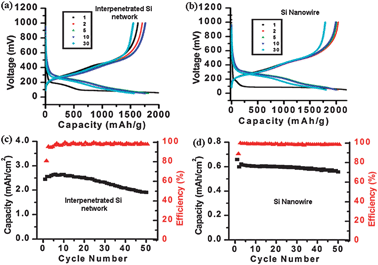 | ||
| Fig. 3 (a) Voltage profile of a Si NP-decorated Si NW network anode. (b) Voltage profile of a control Si NW anode. The control experiment for bare Si NPs shows poor film uniformity due to the low viscosity of the dispersion and only a ∼600 mA h g−1 capacity. (c) Areal capacity of the Si NP–Si NW network anode and its coulombic efficiency. (d) Areal capacity of the Si NW anode and its coulombic efficiency. | ||
To check the morphology of the network after cycling, the pouch cell was dissembled after 20 cycles in the discharged state. The network was soaked in acetonitrile overnight, carefully rinsed with 0.5 M H2SO4 until bubbles disappeared and rinsed with isopropanol in the end. Fig. 4(a) and (b) show the SEM images of the network. The decorated, porous network structure is maintained, where the NPs and NWs are clearly seen. The NW diameters increase largely from ∼100 nm to ∼200 nm. The repeated lithium alloying and dealloying processes have induced nanoporous surfaces on Si as we observed previously.11
 | ||
| Fig. 4 (a) and (b) Top-down view SEM of the Si NP–Si NW network after cycling. The scale bars are 500 μm in (a) and 500 nm in (b), respectively. | ||
In conclusion, we fabricated a Si-NP-decorated Si NW network, where Si NPs are electrically connected to Si NWs. An aqueous, binder-free Si NP dispersion was coated onto VLS-grown Si NW substrates to realize such structures. Such a decorated network greatly increases the areal capacity of Si NW based electrodes, from ∼0.6 mA h cm−2 to ∼2.5 mA h cm−2. The anodes show good cycling performance and maintain the decorated, porous network structures after charging–discharging cycles.
Y. Cui, L. Hu, H. Wu, and L-F. Cui acknowledge the support from the King Abdullah University of Science and Technology (KAUST) Investigator Award (No. KUS-l1-001-12). J. McDonough acknowledges the support from the National Defense Science and Engineering and National Science Foundation Graduate Research Fellowships.
Notes and references
- W. R. Liu, Z. Z. Guo, W. S. Young, D. T. Shieh, H. C. Wu, M. H. Yang and N. L. Wu, J. Power Sources, 2005, 140, 139–144 CrossRef CAS.
- J. P. Maranchi, A. F. Hepp, A. G. Evans, N. T. Nuhfer and P. N. Kumta, J. Electrochem. Soc., 2006, 153, A1246–A1253 CrossRef CAS.
- T. Takamura, M. Uehara, J. Suzuki, K. Sekine and K. Tamura, J. Power Sources, 2006, 158, 1401–1404 CrossRef CAS.
- S. Ohara, J. Suzuki, K. Sekine and T. Takamura, J. Power Sources, 2004, 136, 303–306 CrossRef CAS.
- H. Li, X. J. Huang, L. Q. Chen, Z. G. Wu and Y. Liang, Electrochem. Solid-State Lett., 1999, 2, 547–549 CrossRef CAS.
- H. Kim, M. Seo, M. H. Park and J. Cho, Angew. Chem., Int. Ed., 2010, 49, 2146–2149 CrossRef CAS.
- A. Magasinski, P. Dixon, B. Hertzberg, A. Kvit, J. Ayala and G. Yushin, Nat. Mater., 2010, 9, 353–358 CrossRef CAS.
- C. K. Chan, H. L. Peng, G. Liu, K. McIlwrath, X. F. Zhang, R. A. Huggins and Y. Cui, Nat. Nanotechnol., 2008, 3, 31–35 CrossRef CAS.
- M. H. Park, M. G. Kim, J. Joo, K. Kim, J. Kim, S. Ahn, Y. Cui and J. Cho, Nano Lett., 2009, 9, 3844–3847 CrossRef CAS.
- L. F. Cui, R. Ruffo, C. K. Chan, H. L. Peng and Y. Cui, Nano Lett., 2009, 9, 491–495 CrossRef CAS.
- J. M. J. Choi, S. Jeong, J. Yoo, C. Chan and Y. Cui, Nano Lett., 2010, 10, 1409–1413 CrossRef CAS.
Footnote |
| † This article is part of the ‘Emerging Investigators’ themed issue for ChemComm. |
| This journal is © The Royal Society of Chemistry 2011 |