Control of crystal orientation in soft nanostructures by nanoimprint lithography
Zhijun
Hu
and
Alain M.
Jonas
*
Université catholique de Louvain, Institute of Condensed Matter and Nanosciences, Place Croix du Sud 1, 1348, Louvain-la-Neuve, Belgium. E-mail: alain.jonas@uclouvain.be; Fax: +32 10 451593; Tel: +32 10 473765
First published on 19th November 2009
Abstract
Nanoimprint lithography (NIL) is a low-cost and high resolution technique consisting of replicating the nanofeatures of a hard mold by pressing it into a film of a soft material, in order to create nanostructures of virtually any shape. When NIL is applied to materials capable to self-organize, it may also control their crystallographic orientation and morphology provided imprinting conditions are appropriately selected. The principles governing this ordering involve a decreased nucleation probability in the nanostructures, graphoepitaxial alignment, rheological chain alignment, nanoconfinement in the cavities of the mold, and the effect of pressure on the microstructure of soft materials. The ordering can be rationalized based on the knowledge of the structure of the material and more specifically on the notion of basic structural element of the material. The control over the internal structure of nanomolded materials afforded by NIL translates into improved performance of soft functional nanodevices, as is demonstrated in this highlight.
 Zhijun Hu | Zhijun Hu received his PhD in polymer chemistry and physics in 2004 from Changchun Institute of Applied Chemistry, Chinese Academy of Sciences, under the guidance of Prof. Tianbai He. He moved in 2004 to the University of Louvain in Louvain-la-Neuve (UCLouvain), Belgium, where he worked as post-doctoral researcher in collaboration with Prof. J.-F. Gohy and Prof. A. M. Jonas on block copolymer micelles, fabrication of soft nanostructures and devices by nanoimprint lithography, and polymer crystallization. He was awarded with Prof. Jonas the Runner-up Obducat Prize in 2007 for part of the work presented in this highlight. |
 Alain M. Jonas | Alain M. Jonas is Full Professor of Polymer Science & Engineering at the University of Louvain in Louvain-la-Neuve (UCLouvain), Belgium. He received a PhD in Polymer Science in 1992 from UCLouvain, then worked as post-doctoral scientist in IBM Almaden (USA) before joining the Belgian National Research Foundation in 1994, and then UCLouvain again in 1996. He was Leverhulme visiting professor at the University of Cambridge (UK) in 2007 and was awarded with Dr. Zhijun Hu the Runner-up Obducat Prize in 2007 for part of the work presented in this highlight. |
Introduction
Over the last 50 years, polymers have been developed as efficient structural materials, either by improving chain design using new monomers and more appropriate catalysts, or by tuning their semicrystalline microstructure. Processes such as fiber drawing or film stretching were developed to provide materials displaying excellent mechanical properties in specific spatial directions. Think for instance to polymer packaging films which are currently capable to wrap at least six 1.5 L water bottles and support their weight, an impressive result of improved film blowing technology and associated microstructural changes leading to highly anisotropic mechanical properties.More recently, functional polymers and other soft materials have also been integrated in devices such as photovoltaic cells, light-emitting diodes, or organic transistors and memories.1–3 They are currently establishing themselves as important components for nanotechnology, where the possibility to scale devices down to the single macromolecule level is especially appealing. However, soft materials often suffer from poor performance compared to their inorganic competitors, partly due to a much more disordered random microstructure. For applications, it is therefore critical to control their microstructure and to orient the chains or crystallographic axes in specific directions depending on device geometry. Superficially, the problem is similar to the previous one of improving the mechanical properties of structural polymer materials. However, an important difference exists, because functional devices require materials to be shaped in micro- or nano-objects placed at specific locations relative to other components of the devices, i.e., polymers need to be integrated while controlling their microstructure. In addition, for practical convenience, the developed methods should be rapid and capable to fabricate many devices in parallel.
Traditional methods to control polymer orientation are not easily scalable down to the micro- and nanometer scales. In contrast, most lithographic techniques are ideal to shape and position polymer micro- and nanostructures, but fail to control their internal ordering or are sometimes even detrimental to their functional properties. Bottom-up approaches consisting of first fabricating nanostructures of high internal order and then assembling them are attractive for the long term, but are not mature enough for practical applications. In this highlight, we review the recent work of a small number of research groups on the use of nanoimprint lithography (NIL) to nanoshape soft materials while simultaneously controlling their internal order and spatial position. NIL is first briefly described, then the principles behind the control by NIL of the microstructure of organic soft materials are rationalized and illustrated by specific examples.
Nanoimprint lithography - NIL
The embossing of soft materials such as paper, clay or wax by hard seals is a well-known shaping method, dating back to the Ancient Egypt and Mesopotamia kingdoms and to the first Chinese empire. This method of embossing was transferred to nanotechnology 5000 years after its initial discovery, and is currently known as nanoimprint lithography (NIL),4 hot embossing5 or nanoembossing.6 Since its first disclosure by S. Chou,4,7 the method has attracted strong interest and is currently considered as one of the possible industrial lithographic options for reaching feature sizes below 30 nm.8 Its main advantages are a limited cost, a high throughput and the possibility to reach very small feature sizes. Because NIL was reviewed extensively before,9–15 it will not be discussed in detail in the present context. We thus concentrate on the most important features of the method required to understand the sequel.NIL replicates a relief pattern in a heated thermoplastic or in a thermosetting polymer by mechanical deformation, rather than by the local photo- or electro-chemical modification of the resist as with photo- and electron beam lithography. In its original version (Fig. 1), a thin film of an amorphous thermoplastic polymer is spin-cast onto a flat surface. The polymer film is heated ∼70 °C above its glass transition temperature, Tg. A rigid mold bearing nanoscale features and an anti-adhesive coating is then pressed into the fluid polymer film under a pressure of 10–100 bar. The polymer film is finally hardened by decreasing the temperature below Tg, and the mold is removed. A topological contrast is thus created in the polymer film after imprinting. A thin residual layer of polymer is usually left between the fragile protrusions of the mold and the substrate to prevent the protrusions from crashing on the hard substrate.12 As for most advanced lithographic techniques, NIL requires to fabricate a master by a slow, expensive but efficient technique such as electron-beam lithography; this master is then replicated numerous times by a less expensive, more rapid methodology. This is similar to classical printing or stencil techniques, which also need to create a template from which many copies are subsequently produced.
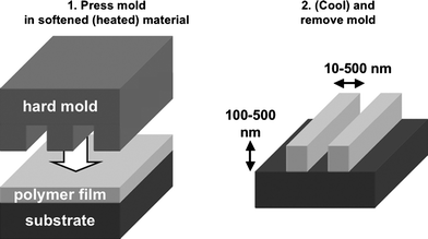 | ||
| Fig. 1 Scheme of nanoimprint lithography. | ||
The imprinting resists used in NIL are typically thermoplastic amorphous homopolymers such as poly(methyl methacrylate) (PMMA), polycarbonate (PC) and polystyrene (PS). However, because NIL is essentially a molding technique acting at the nanometer scale, it can also be used to directly shape functional polymers into nanowires, nanopillars or other useful nanoobjects. Most importantly, when applied to soft materials, NIL also controls ordering processes at the nanometer scale. In this case, not only is the shape of the nanoobjects controlled during embossing, but also their microstructure, giving rise to enhanced performance compared to unprocessed materials.
Ordering soft materials by NIL
We first take semicrystalline polymers to illustrate the reasons why NIL may affect ordering. These materials crystallize in lamellar crystals of ∼10 nm thickness having lateral sizes in the micrometer range (Fig. 2). The chains are perpendicular or slightly inclined to the basal surfaces of the lamellae, and either fold back in the same lamella or reenter a neighboring lamella when emerging from the crystal surface.16,17 Successive lamellae are separated by amorphous interlayers, which accumulate folds, loose loops, tie segments, and dangling ends of the chains.18,19 The crystallization process starts by nucleation from a central seed, most often an impurity,20 from which a complex assembly of lamellae forms by crystal growth, branching and splaying.21 The resulting spherulite has a radius in the micrometer range, and the lamellae are globally radial within the spherulites, although more complex packing schemes exist. At the supraspherulitic scale, semi-crystalline polymers are thus isotropic and consist of an intricate mixture of crystallized and amorphous nanoregions. Therefore, their properties average different phases over all possible orientations, and include components resulting from the numerous crystal/amorphous interfaces present in a spherulite. This significantly reduces the performance of such materials. | ||
| Fig. 2 Schematic illustration of the hierarchical microstructure of semicrystalline polymers crystallized from the isotropic melt. | ||
Consider now the potential effects of NIL on this complex morphology. Embossing is performed in the molten state, but the polymer crystallizes in the mold during cooling.
1. The nucleation process might be affected, because the mold splits the melt into a very large number of small cavities. The probability to find a heterogeneous nucleating seed in a cavity depends on the product between the volume of each nanocavity and the number density of seeds in the melt. Therefore, this probability may be well below 1 if cavities are small enough. In such a case, crystallization will occur in a nanocavity either when a nucleating germ forms spontaneously, a process called homogeneous nucleation rarely encountered in practice when crystallizing bulk polymers; or when a crystal propagates from the outside into the nanocavity, which is only possible if the cavity is not totally isolated and if a nearby crystal grows in the proper orientation. The situation is thus similar to the one encountered when crystallizing polymers in microdroplets,22,23 in microdomains of phase-separated block copolymers24–26 or in the nanopores of membranes,27,28 cases for which retarded crystallization and preferred orientation are often reported. Identical effects are to be expected in NIL as well.
2. The crystal growth process might also be affected. It was reported in Russia in 1972,29 and rediscovered later in the USA,30 that topographically-patterned amorphous surfaces may induce preferential orientation of growing crystals, provided the symmetry of the topography be adapted to the habit of the growing crystals. This phenomenon is known as “graphoepitaxy” or “artificial epitaxy”,31,32 with reference to the epitaxy of crystals on crystalline substrates where matching between the lattice planes of the growing crystal and of the substrate provides for preferential orientation. In graphoepitaxy, however, the matching occurs at a higher scale and does not require a crystalline substrate. Key thermodynamic parameters are the shape of the growing entity and the symmetry of the substrate topography, as well as the surface tensions and surface tension anisotropies of the crystal/substrate and melt/substrate interfaces, which dictate the energy balance of the growing system.33 On the kinetic side, the growth rates of the crystal along specific crystalline directions are also important parameters, because they control the crystal shape, hence the graphoepitaxial matching. In the present context, the topography of the NIL mold may thus control graphoepitaxially the crystallization process of the polymer, resulting in a preferential alignment of specific crystallographic directions with respect to the nanofeatures of the mold.
3. A third factor which could affect the crystallization process in a NIL experiment is the degree of chain alignment resulting from the melt embossing process. Polymers are viscoelastic fluids, which keep for long times the partial memory of the squeeze flow experienced during the imprinting. In addition, polymer chains tend to align along flow lines during processing. This favors oriented crystallization34–36 and the emergence of specific morphologies such as “shish-kebabs”.37,38 In NIL, the residual degree of chain alignment will depend on factors affecting rheology, such as the molar mass of the polymer, its previous processing history, and its annealing time in the melt before crystallization. In addition, molecular confinement of the chains in a thin film may lead to a substantially perturbed rheological behavior.39
4. A fourth factor is confinement itself. Most macromolecules have radii of gyration in the same range as the thickness of films and the size of the mold features, resulting in strong confinement of the chains. There is currently an ongoing discussion regarding the way confinement affects polymer properties such as glass transition and segmental mobility40,41 or whole chain motion.39 Conflicting results have been reported; at any rate, one should keep in mind that the conformation and dynamic properties of confined polymers may be substantially different in a nanocavity than in the bulk, which is likely to modify their crystallization behavior as well. For instance, chains need to fold back and forth to form lamellar crystals (Fig. 2). If this occurs in a space only slightly larger than the intrinsic lamellar thickness, perturbations of the crystallization process are obviously to be expected.
5. Finally, a last factor to take into account is the effect of pressure on polymer crystallization. Polymer crystals formed under high pressure may differ substantially from those obtained at ambient pressure; for instance, extended chain crystals are obtained when crystallizing polyethylene42 or poly(ethylene terephthalate)43 at pressures of a few kbar or above. The pressures used in NIL (10–100 bar) are much smaller, but might already affect morphology when combined with confinement effects.
What is true for polymer crystallization should also be valid for other supramolecular assembly processes, such as the formation of liquid crystalline domains or the ordering of block copolymer mesophases. Below, we show that NIL indeed orients crystals and chains in specific directions, resulting in favorable cases in a significant improvement of the performance of nanodevices. This is demonstrated for amorphous rigid polymers, liquid crystalline polymers, semicrystalline polymers, and phase-separated block copolymers.
The results are divided in two classes, NIL under either full or partial confinement. In the first case, the starting film thickness and the height of the protrusions on the mold are such that the mold can touch the surface of the substrate if pressed strongly enough (Fig. 3). For a mold having a protruding surface fraction σ, each protrusion being of height h, full confinement occurs when the starting film thickness d < (1 − σ)h. In this case, each recess of the mold is effectively isolated from other recesses. In contrast, when d > (1 − σ)h, a continuous residual film remains between the substrate and the protruding features of the mold, no matter how hard the mold is pressed in the film.44 In this case, information on the ordering process may propagate from recess to recess, which has significant consequences on the global ordering of the sample.
 | ||
| Fig. 3 Two modes of nanoimprinting leading to different microstructures after imprinting. | ||
Ordering under partial confinement
An experimental demonstration of molecular alignment by NIL line grating molds was first obtained for chromophores dissolved in a PMMA resist.45 Polarized photoluminescence and absorption measurements indicated that the dye molecules are aligned after imprint with their long axis along the grating lines. The fluorescence anisotropy R quantifies the degree of alignment by comparing the fluorescence emission polarized parallel to the grating lines and perpendicular to them. R values of 0 and 1 correspond to complete isotropy and complete alignment, respectively. For this specific example, R values of 0.1–0.2 indicated that the polymer flow alone is only able to align moderately the dye molecules.For semi-crystalline polymers crystallized in partial confinement with NIL line grating molds, no or very limited preferential orientation of polymer crystals occurs.46,47 Thin films of poly(vinylidene fluoride) (PVDF, α phase) crystallize in their usual spherulitic morphology and are apparently insensitive to the presence of the grooves of the NIL molds.46 The crystalline lamellae propagate from groove to groove (Fig. 4), and the electron diffraction patterns do not show preferred orientation relative to the line grating direction. This has to be ascribed to fast crystal growth in the thin residual film below the protrusions of the mold, from which crystallization propagates into the linear grooves of the mold. The final morphology is thus not controlled by the mold, but mainly by the residual film. Similar results were obtained for poly(ethylene oxide) (PEO),47 although partial elongation of the crystalline lamellae along the grooves of the mold was sometimes observed. These results indicate that graphoepitaxy and/or chain alignment do not occur for semicrystalline polymers processed by NIL in partial confinement.
 | ||
| Fig. 4 AFM height image of a thin film of PVDF nano-imprinted in partial confinement, showing the propagation of crystallographic information from groove to groove. The average orientation of crystalline lamellae in the spherulite is indicated by arrows. | ||
The situation appears to be different when imprinting a low molar mass liquid crystalline conjugated polymer, poly(9,9-dioctylfluorene-co-benzothiadiazole) (F8BT), in its liquid crystalline nematic mesophase.48,49 This green-light-emitting polymer displayed after imprinting R values as large as 0.97, indicating that most polymer chains are aligned parallel to the line grating direction. The order parameter R decreases for thicker films, suggesting that the ordering starts from the surface of the mold and progressively vanishes when going down into the residual film. Light-emitting diodes (PLEDs) were successfully built based on nanoimprinted F8BT, giving rise to the emission of preferentially linearly-polarized light; and a field-effect transistor (FET) was also realized, with a measured hole mobility 10–15 times larger parallel to the grating lines than perpendicular to them. These results illustrate the beneficial impact of aligning molecules, as far as charge mobility or emission polarization is concerned. It should however be noted that NIL failed to align a similar light-emitting conjugated polymer, poly(9,9-dioctylfluorene) (F8) also displaying a liquid crystalline nematic mesophase.50 This was tentatively ascribed to the higher molar mass (hence larger viscosity) of this polymer compared to F8BT. Clearly, NIL under partial confinement is able to align liquid crystalline polymers in favorable circumstances; however, further work is required to fully understand the factors which control this alignment, that might be similar to the ones driving the alignment of liquid crystals on buffing layers.51
Ordering under full confinement
The previous results show that spherulites of semicrystalline polymer grow relatively unaffected when NIL is performed in partial confinement. Because the size of spherulites is governed by the number density of nucleating seeds, significant perturbations of the crystallization process can be expected as soon as the melt is split in cavities of size much smaller than this natural length scale. Stated otherwise, if the melt is split in isolated cavities numerous enough to have a low probability to find a nucleating seed in each of them, the whole process of crystallization will be strongly perturbed. Based on this simple idea, we devised experiments where the starting film thickness was small enough for the NIL mold to enter in contact with the substrate, conditions denoted as ‘full confinement’ hereafter (Fig. 3, right). In this case, the propagation of information from groove to groove is suppressed, and complete graphoepitaxial alignment may even happen as will be demonstrated below. It is critical to realize that graphoepitaxial alignment occurs at some stage during the formation of a structure, depending on the details of the processing history. It may thus orient a growing crystal, or a liquid crystalline domain, or even a single molecule, depending on the basic structural element which interacts with the mold and the kinetics of growth. The notion of basic structural element is thus key to understand and reconcile results published in the literature.When a semi-crystalline polymer crystallizes from the isotropic melt in a line grating mold, the basic structural element to consider is the nascent crystal. Because polymer crystals are elongated along their fast growth axis direction, alignment of this crystal axis along the grating lines is favored for geometrical reasons. This is the case for PVDF crystallized in complete confinement in its orthorhombic α form,46 whose fast b-axis aligns parallel to the grooves of the NIL mold (Fig. 5a). Interestingly, when NIL molds containing curved grooves are used, the b-axis follows these curved tracks.52 This can only be possible if the resulting curved nanowires are polycrystalline. Note that graphoepitaxy in linear channels only aligns one crystal axis, leaving open the issue of the rotation of the crystal about this axis. It was found for NIL-imprinted α-PVDF that the chain c-axis is perpendicular to the substrate for films below about 100 nm (flat-on lamellae), whereas in thicker films the crystals have their chain c-axis parallel to the substrate (edge-on lamellae).52 In both cases, however, the b-axis remains parallel to the grooves. The variation from a flat-on to an edge-on orientation upon increasing film thickness is frequent with polymers and was tentatively rationalized recently.53
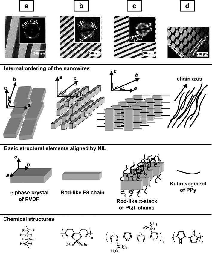 | ||
| Fig. 5 Selected examples of functional polymers aligned preferentially by NIL in full confinement. The upper row shows transmission electron microscopy images of nanowires (a) of PVDF, (b) of electroluminescent F8 and (c) of semi-conducting PQT, and (d) a polarized microscopy image of birefringent arrays of nanowires of conducting PPy (the nanowire axes are at 45° with respect to the polarizer and analyzer directions). Insets in (a–c) are the corresponding electron diffraction patterns, showing the crystal setting relative to the line grating direction of the molds. The second row is a schematic drawing of the internal structure of the nanowires, based on the experimental data. The third row presents schematic drawings of the basic structural elements aligned during imprinting (a nascent crystal for semi-crystalline PVDF, rod-like chains for the nematic liquid crystalline phase of F8, a supramolecular rod of π-stacked chains in the liquid crystalline phase of PQT, and chain segments of the amorphous PPy). The fourth row presents the chemical structures of the compounds. | ||
For polymers imprinted in a liquid crystalline phase, then cooled into a crystalline phase, the basic structural element to consider differs depending on the detailed microstructure of the liquid crystalline phase. Poly(9,9-dioctylfluorene) (F8) was imprinted in its nematic liquid crystalline phase, a phase in which chain axes tend to orient parallel to a director with no other type of long-range ordering.54 Thus, the basic structural element is simply a rod-like chain, which for entropic and geometrical reasons aligns parallel to the grooves. After cooling and crystallization, the preferential ordering is maintained, and the chain axis (which is the c-axis in the low temperature crystal phase) remains parallel to the grooves, hence to the axis of the resulting nanowire (Fig. 5b). The preferential alignment translates into polarized light emission, with a R factor of 0.65–0.7 testifying for a high degree of ordering. This is in stark contrast with the absence of preferential ordering reported when F8 was imprinted in partial confinement,50 and shows the importance of full confinement for NIL-induced graphoepitaxy.
The semi-conducting poly(3,3‴-didodecyl-quaterthiophene) (PQT) was also imprinted in its liquid crystalline phase under full confinement.54 PQT chains form in the liquid crystalline phase supramolecular rod-like nanostructures wherein extended chains pack with their π-stacking direction along the rod axis. The basic structural element is thus the rod-like nanostructure, whose long axis aligns parallel to the grooves of the mold. As a consequence, the π-stacking direction is parallel to the axis of the imprinted nanowire, and this orientation is kept when the polymer crystallizes upon cooling. Therefore, the b-axis of the crystal, which is the π-stacking direction, is similarly aligned at the end of the process (Fig. 5c), whereas the chain c-axis direction was found to be perpendicular to the nanowire axis. The situation is therefore entirely different from F8, where the chain axis was aligned parallel to the nanowire axis. In the present case, this specific crystal setting is interesting for applications, because the PQT b-axis is the axis of high carrier mobility. A nanowire-based field-effect transistor was realized by nanoimprint, and it was demonstrated that the hole mobility is increased by a factor of 1.7 along the nanowire axis compared to an isotropic PQT film. This increase is close to the factor of 2 expected upon passing from an isotropic to a uniaxial bidimensional material (corresponding to the reciprocal of the average value of the square of the cosine of the angle describing the orientation of the b-axis).
For rigid conjugated amorphous polymers, which cannot crystallize and do not adopt a liquid crystalline phase, the basic structural element to consider during imprinting is simply their Kuhn segment. Conjugated polymers have large persistence lengths and therefore long Kuhn segments. These will tend to align parallel to the groove direction during imprinting. The resulting nanowire thus contains chains whose axes are parallel to the nanowire axis, which is favorable for conductivity. For polypyrrole (PPy) for instance, the axial conductivity was improved by a factor of 1.7 in the imprinted nanowires compared to the isotropic film,54 and this was again correlated to the preferential chain alignment observed by birefringence measurements (Fig. 5d).
A final example of graphoepitaxial alignment by NIL in full confinement is provided by the supramolecular assembly of a phase-separated block copolymer.55 The selected poly(styrene)-block-poly(methyl methacrylate) (PS-b-PMMA) copolymer consists of flexible amorphous blocks, which do not align by themselves. However, due to the microphase separation of the two incompatible blocks, the PMMA regions form nanocylinders located on the nodes of a hexagonal lattice, within a continuous PS matrix.56 Such microphase-separated copolymers are known to form graphoepitaxially-oriented supramolecular crystals.57–59 They should thus also align in NIL. Here, the proper structural element is the unit cell of the supramolecular crystal, whose unit cell parameters are in the 10 nm range and above. The axes of the block copolymer unit cell were indeed found to be parallel to the direction of the grooves of the mold, although which axis is parallel to the grooves depends on the thickness of the starting block copolymer film.55 However, the regularity of the packing was limited, most probably because the dimensions of the grooves were not exactly adapted to the natural period of the block copolymer.
So far, all examples given above refer to line gratings as molds. Other feature shapes can be selected, but the success or failure of graphoepitaxy will depend on the matching between the intrinsic size of the basic structural element and the shape of the nanofeatures of the mold.31 When square cavities are selected instead of grooves, it is obvious that no preferential alignment in the plane of the film can be expected. However, this does not preclude ordering effects from appearing. This was reported for a statistical poly(vinylidene fluoride-stat-trifluoroethylene) copolymer (P(VDF-TrFE)), which was imprinted in its paraelectric liquid crystalline phase, then crystallized by cooling into the ferroelectric pseudo-hexagonal β phase.60 The mold consisted of square nanocavities about 100 nm in lateral size, allowing to shape the polymer film into a dense array of nanosquares. As expected, there was no preferential orientation in the plane of the film after imprint; however, the c axis about which the polar b axis rotates was aligned dominantly horizontally, and each 100 nm side square was found to consist of a single ferroelectric domain. This resulted in a much lower voltage than usually required to switch the direction of the electrical dipole moment. Interestingly, if nanoimprinting is performed with micro- instead of nanometer-sized cavities, no preferential orientation of the b-axis is noted, and the performance of the device is not improved compared to the macroscopic film.61 This underlines the importance of confining crystallization to dimensions comparable to or below the intrinsic crystal size for optimal results. This intrinsic size is (150 nm)2 for a P(VDF-TrFE) sample processed as in NIL but in the absence of a mold. In order to control the organization process, one should therefore use molds having cavities smaller than this natural length scale. This example also illustrates that the combination of shaping and crystalline improvement afforded by NIL is extremely useful for device development. Indeed, high-density arrays of ferroelectric polymer crystals exhibiting a low switching voltage were produced by NIL in the present case, that could lead to the development of cheap organic random-access memories.
Conclusions
Nanoimprint lithography is a well-established lithographic technique, which is expected to play a significant role in the development of semiconductor technology. It has been observed recently that when applied to soft materials capable to self-organize, NIL is also capable to orient graphoepitaxially the basic structural elements of the material, provided it is performed under full confinement. In much rarer cases such as for liquid crystals of low molar mass, partial confinement may also lead to preferential crystallographic orientation. The control over the internal structure of nanomolded materials often translates into improved device performance. For instance, it was shown that NIL-induced ordering results in polarized light emission for electroluminescent polymers, increased mobility of charge carriers in semi-conducting polymers, increased conductance of conjugated conducting polymers, or easier switching of permanent electrical dipole moments for ferroelectric polymers.In this highlight, we provided the reader with a series of reasons explaining why NIL under complete confinement should affect ordering processes: decreased nucleation probability in small recesses, graphoepitaxial alignment, rheological chain alignment, nanoconfinement effects and pressure are all important factors to consider. How each of these factors is playing a role for a specific material has still to be fully understood, and much more research is required before being able to obtain a complete picture. Meanwhile, it is still possible to rationalize the principles governing orientation based on the knowledge of the structure of the material and on the notion of basic structural element. This was attempted in the present highlight as summarized in Fig. 5. These simple rules should help device designers to predict the effects of NIL on the microstructure of materials, and therefore to use fully the power of this promising nanoprocessing method when applied to soft materials.
Notes and references
- G. Malliaras and R. Friend, Phys. Today, 2005, 58, 53 CAS.
- T. W. Kelley, P. F. Baude, C. Gerlach, D. E. Ender, D. Muyres, M. A. Haase, D. E. Vogel and S. D. Theiss, Chem. Mater., 2004, 16, 4413 CrossRef CAS.
- Q.-D. Ling, D.-J. Liaw, C. Zhu, D. S.-H. Chan, E.-T. Kang and K.-G. Neoh, Prog. Polym. Sci., 2008, 33, 917 CrossRef CAS.
- S. Y. Chou, P. R. Krauss and P. J. Renstrom, Appl. Phys. Lett., 1995, 67, 3114 CrossRef CAS.
- L. J. Heyderman, H. Schift, C. David, J. Gobrecht and T. Schweizer, Microelectron. Eng., 2000, 54, 229 CrossRef CAS.
- V. Studer, A. Pepin and Y. Chen, Appl. Phys. Lett., 2002, 80, 3614 CrossRef CAS.
- S. Y. Chou, P. R. Krauss and P. J. Renstrom, Science, 1996, 272, 85 CAS.
- International Technology Roadmap for Semiconductors, 2007 edition (http://www.itrs.net) Search PubMed.
- C. M. Sotomayor Torres, ed., Alternative lithography. Unleashing the potentials of nanotechnology. Kluwer Academic/Plenum, New York, 2003 Search PubMed.
- L. J. Guo, J. Phys. D: Appl. Phys., 2004, 37, R123 CrossRef CAS.
- M. D. Stewart and C. G. Willson, MRS Bull., 2005, 30, 947 CAS.
- L. J. Guo, Adv. Mater., 2007, 19, 495 CrossRef CAS.
- D. J. Resnick, in Microlithography science and technology, ed. K. Suzuki and B. W. Smith, Taylor & Francis, Boca Raton, 2007, pp. 465–499 Search PubMed.
- H. Schift and A. Kristensen, in Springer handbook of nanotechnology, ed. B. Bushan, Springer, Berlin, 2nd edn, 2007, pp. 239–278 Search PubMed.
- H. Schift, J. Vac. Sci. Technol., B, 2008, 26, 458 CrossRef CAS.
- U. W. Gedde, Polymer physics, Chapman & Hall, London, 1995 Search PubMed.
- G. Reiter and G. R. Strobl, eds, Progress in understanding of polymer crystallization. Lect. Notes Phys. 714, Springer, Berlin, 2006 Search PubMed.
- L. Mandelkern, Faraday Discuss. Chem. Soc., 1979, 68, 310 RSC.
- S. Gautam, S. Balijepalli and G. C. Rutledge, Macromolecules, 2000, 33, 9136 CrossRef CAS.
- B. Wunderlich, Macromolecular physics. Vol. 2. Crystal nucleation, growth, annealing, Academic Press, New York, 1976 Search PubMed.
- D. C. Bassett, Crit. Rev. Solid State Mat. Sci., 1984, 12, 97 Search PubMed.
- R. L. Cormia, F. P. Price and D. Turnbull, J. Chem. Phys., 1962, 37, 1333 CAS.
- M. V. Massa and K. Dalnoki-Veress, Phys. Rev. Lett., 2004, 92, 255509 CrossRef.
- G. Reiter, G. Castelein, J. U. Sommer, A. Rottele and T. Thurn-Albrecht, Phys. Rev. Lett., 2001, 87, 226101 CrossRef CAS.
- Y. L. Loo, R. A. Register and A. J. Ryan, Macromolecules, 2002, 35, 2365–74 CrossRef CAS.
- A. J. Muller, V. Balsamo, M. L. Arnal, T. Jakob, H. Schmalz and V. Abetz, Macromolecules, 2002, 35, 3048 CrossRef.
- M. Steinhart, P. Göring, H. Dernaika, M. Prabhukaran, U. Gösele, E. Hempel and T. Thurn-Albrecht, Phys. Rev. Lett., 2006, 97, 027801 CrossRef.
- E. Woo, J. Huh, Y. G. Jeong and K. Shin, Phys. Rev. Lett., 2007, 98, 136103 CrossRef.
- N. N. Sheftal and N. A. Bouzynin, Vestn. Mosk. Univ. Ser. Geol., 1972, 27, 102 Search PubMed.
- H. I. Smith and D. C. Flanders, Appl. Phys. Lett., 1978, 32, 349 CrossRef CAS.
- E. I. Givargizov, in Handbook of crystal growth, eds. T. Donald and J. Hurle, Elsevier, Amsterdam, 1994, vol. 3, pp. 941–995 Search PubMed.
- E. I. Givargizov, J. Cryst. Growth, 2008, 310, 1686 CrossRef CAS.
- P.-O. Mouthuy, S. Melinte, Y. H. Geerts and A. M. Jonas, Nano Lett., 2007, 7, 2627 CrossRef CAS.
- R. L. Miller, ed., Flow-induced crystallization in polymer systems, Gordon & Breach, New York, 1979 Search PubMed.
- G. Kumaraswamy, A. M. Issaian and J. A. Kornfield, Macromolecules, 1999, 32, 7537 CrossRef CAS.
- R. H. Somani, B. S. Hsiao, A. Nogales, S. Srinivas, A. H. Tsou, I. Sics, F. J. Balta-Calleja and T. A. Ezquerra, Macromolecules, 2000, 33, 9385 CrossRef CAS.
- G. Eder, H. Janeschitz-Kriegel and G. Krobath, Prog. Colloid Polym. Sci., 1989, 80, 1 CAS.
- S. Kimita, T. Sakurai, Y. Nozue, T. Kasahara, N. Yamaguchi, T. Karino, M. Shibayama and J. A. Kornfield, Science, 2007, 316, 1014 CrossRef CAS.
- H. D. Rowland, W. P. King, J. B. Pethica and G. L. W. Cross, Science, 2008, 322, 720 CrossRef CAS.
- C. J. Ellison and J. M. Torkelson, Nat. Mater., 2003, 2, 695 CrossRef CAS.
- M. Alcoutlabi and G. B. McKenna, J. Phys.: Condens. Matter, 2005, 17, R461 CrossRef CAS.
- B. Wunderlich, Pure Appl. Chem., 1972, 31, 49 CrossRef CAS.
- A. Siegmann and P. J. Harget, J. Polym. Sci., Polym. Phys. Ed., 1980, 18, 2181 CrossRef CAS.
- H. Schift and L. J. Heyderman, in Alternative lithography. Unleashing the potentials of nanotechnology, ed. C. M. Sotomayor Torres, Kluwer Academic/Plenum, New York, 2003, pp. 47–76 Search PubMed.
- J. Wang, X. Sun, L. Chen, L. Zhuang and S. Y. Chou, Appl. Phys. Lett., 2000, 77, 166 CrossRef CAS.
- Z. Hu, G. Baralia, V. Bayot, J.-F. Gohy and A. M. Jonas, Nano Lett., 2005, 5, 1738 CrossRef CAS.
- B. C. Okerberg, C. L. Soles, J. F. Douglas, H. W. Ro, A. Karim and D. R. Hines, Macromolecules, 2007, 40, 2968 CrossRef CAS.
- Z. Zheng, K.-H. Yim, M. S. M. Saifullah, M. E. Welland, R. H. Friend, J.-S. Kim and W. T. S. Huck, Nano Lett., 2007, 7, 987 CrossRef CAS.
- S. A. Schmid, K. H. Yim, M. H. Chang, Z. Zheng, W. T. S. Huck, R. H. Friend, J. S. Kim and L. M. Herz, Phys. Rev. B: Condens. Matter Mater. Phys., 2008, 77, 115338 CrossRef.
- M. H. Song, B. Wenger and R. H. Friend, J. Appl. Phys., 2008, 104, 033107 CrossRef.
- M. F. Toney, T. P. Russell, J. A. Logan, H. Kikuchi, J. M. Sands and S. K. Kumar, Nature, 1995, 374, 709 CrossRef CAS.
- Z. Hu and A. M. Jonas, unpublished work.
- Y. Wang, C. M. Chan, K. M. Ng and L. Li, Macromolecules, 2008, 41, 2548 CrossRef CAS.
- Z. Hu, B. Muls, L. Gence, D. A. Serban, J. Hofkens, S. Melinte, B. Nysten, S. Demoustier-Champagne and A. M. Jonas, Nano Lett., 2007, 7, 3639 CrossRef CAS.
- H.-W. Li and W. T. S. Huck, Nano Lett., 2004, 4, 1633 CrossRef CAS.
- I. W. Hamley, The physics of block copolymers, Oxford University Press, Oxford, 1998 Search PubMed.
- J. Y. Cheng, F. Zhang, H. I. Smith, G. J. Vancso and C. A. Ross, Adv. Mater., 2006, 18, 597 CrossRef CAS.
- I. Bita, J. K. W. Yang, Y. S. Jung, C. A. Ross, E. L. Thomas and K. K. Berggren, Science, 2008, 321, 939 CrossRef CAS.
- S. Park, D. H. Lee, J. Xu, B. Kim, S. W. Hong, U. Jeong, T. Xu and T. P. Russell, Science, 2009, 323, 1030 CrossRef CAS.
- Z. Hu, M. Tian, B. Nysten and A. M. Jonas, Nat. Mater., 2009, 8, 62 CrossRef CAS.
- L. Zhang, S. Ducharme and J. Li, Appl. Phys. Lett., 2007, 91, 172906 CrossRef.
| This journal is © The Royal Society of Chemistry 2010 |