The impact of erbium incorporation on the structure and photophysics of silicon–germanium nanowires†
Ji
Wu
a,
Monika
Wieligor
b,
T. Waldek
Zerda
b and
Jeffery L.
Coffer
*a
aDepartment of Chemistry, Texas Christian University, Fort Worth, TX 76129, USA. E-mail: j.coffer@tcu.edu
bDepartment of Physics, Texas Christian University, Fort Worth, TX 76129, USA
First published on 8th October 2010
Abstract
In this paper, we report multi-step processes for the fabrication of Er3+-doped SiGe nanowires (NWs) and characterization of their emissive properties. Three different alloyed architectures are obtained by altering the deposition sequences of Si and Er3+ on a Ge core NW, each involving a fixed concentration of these three elements. The deposition of Si onto the Ge NW core, followed by an Er3+-rich layer on the outermost surface, permits facile formation of a SiGe alloy given the lack of an erbium diffusion barrier; yet clustering of the erbium centers on the NW surface produces the weakest emitter. For nanowires prepared by co-depositing Si and Er3+ on top of the Ge core, the presence of impurity Er3+ ions greatly reduces the alloying rate of Si and Ge such that less Si can diffuse into the Ge core. For this structure, the reduction of Er–Er interactions by a polycrystalline Si shell results in the strongest emission at 1540 nm. If an Er3+ layer is inserted between the Ge and Si layers (a sandwich structure), it is found that Er3+ ions diffuse preferentially into the SiGe core instead of the silicon-rich shell, with a correspondingly weaker luminescence intensity. A combination of high resolution transmission electron microscopy, energy dispersive X-ray mapping, micro-Raman spectroscopy, and photoluminescence spectroscopy are employed to derive these conclusions.
Introduction
Silicon-germanium (SiGe) alloys are currently of great interest due to their extensive applications in the fields of microelectronics and microoptoelectronics.1 These alloys have useful properties of a tunable band gap and variable refractive index that are determined by the ratio of germanium (Ge) to silicon (Si). Compared with pure Si, SiGe alloys have much higher carrier mobilities, which can greatly enhance the device performance.2 Furthermore, SiGe materials that could be grown epitaxially on Si wafers are fully compatible with the silicon microelectronics industry.3 A number of applications are envisioned as a consequence: microwave and millimetre-wave applications;4 quantum cascade terahertz lasers;5,6 and enhanced p-type field-effect transistors (FETs).2,7The fabrication of one-dimensional (1D) SiGe nanowires (NWs) is a fundamental step to evaluate their merit as potential building blocks for nanoscale devices.8 One very important potential application for nanodevices is the processing and transmission of optical signals in waveguides. It requires efficient light emitters in the 1.5 µm spectral region. The incorporation of Er3+ ions in such structures can make SiGe an efficient light emitter at this wavelength due to the intra-4f 4I13/2 → 4I15/2 transition associated with this rare earth center.
As a strategy toward the bottom-up fabrication of silicon-compatible 1.54 µm light emitters, waveguides, and detector building blocks, our group has explored the preparation and optical properties of Er3+-doped Si nanocrystals (NCs)9–12 as well as Er3+-surface enriched Si and Ge NWs.13–15 Although Er3+-doped Ge NWs show better performance in terms of light emission intensity at 1.54 µm relative to Er3+-doped Si NW analogs,14 Ge NWs are readily oxidized due to their large surface/volume ratio and thermodynamic instability, which can fundamentally limit their functionality.16 In this regard, the incorporation of Si into Ge NWs should circumvent this problem by forming stable SiGe alloys that passivate the reactive surface.
In this paper, we report multi-step processes for the fabrication of Er3+-doped SiGe NWs and characterization of their optical properties. Three different alloyed architectures are obtained by altering the deposition sequence of Si and Er3+ on a Ge NW core; after each unique sequence, alloying is obtained by thermal annealing at elevated temperatures. The structure of products obtained from these reactions is interpreted considering the role of erbium altering the diffusion between the Ge and Si layers and the subsequent impact of thermal treatment on erbium light emission. A combination of electron microscopies—transmission electron microscopy (TEM), high resolution transmission electron microscopy (HREM), conventional scanning electron microscopy (SEM), field emission scanning electron microscopy (FE SEM), in concert with energy dispersive probe mapping and Raman microanalyses—are used for this purpose.
Results
General overview of the fabrication approach
The overall synthetic strategy for Er3+-doped SiGe NWs is illustrated in Fig. 1. In this specific strategy three different variants of Er3+-doped SiGe NWs were grown; each type of doped NW structure is based on a Ge core NW fabricated by a simple vapor-transport method as reported previously.15 | ||
| Fig. 1 General synthetic routes to Er-doped SiGe NWs. | ||
With regard to Si and Er incorporation, three permutations are possible: (1) Si deposition followed by Er (an ‘Erbium surface-rich’ NW); (2) Er, then Si (a sandwich configuration), or (3) concurrent deposition of both species on the Ge NW core (a ‘Si & Er co-deposited’ structure). Several intrinsic properties of erbium are relevant to this strategy. Erbium possesses a very low solubility in crystalline Si, but the affinity of this rare earth for oxygen can significantly improve this parameter through complex formation.17 Furthermore, the presence of oxygen can also strongly enhance erbium luminescence by increasing the percentage of optically active erbium ions, and reduce temperature-quenching effects.18 Literature data are also available for the thermally driven diffusion of erbium in silicon in thin film form with the presence of oxygen.19 Hence the above strategy was pursued given the expectation that erbium ions will alter the rate of alloy formation and stoichiometry of the resultant products formed.
Structural characterization of the 3 different NW permutations
 | ||
| Fig. 2 (a) SEM image of the “sandwich” structure Er3+-doped SiGe NWs (scale bar = 1 µm); (b) EDX spectrum of the NWs; (c) TEM image of a typical NW with ∼30 nm SiGe core and a ∼15 nm shell; (d) EDX linescans of the NW shown in (c). | ||
EDX linescans of an individual NW (Fig. 2d) show that the dark core is Ge-rich, and the light-contrast shell is predominantly composed of Si and some O (not shown). Germanium can also be found in the outer shell near the core/shell interface. The Er concentration is almost constant throughout the SiGe core with only a slightly higher value at the interface between the core and the shell. There is no detectable Er in the outer silicon shell. Three distinct regions on the nanowires annealed at 600 °C for 1 h in N2 were detected by performing quantitative EDX analyses (ESI†). One is the center of the NW that has the lowest Er concentration (2.6%); another region is located at the interface between the bright shell and the dark core, which has a higher Er concentration (6.7%); the third one is the shell, with negligible Er present. This result is interpreted in terms of a preferential diffusion of erbium into the crystalline SiGe core instead of the shell. Very similar results were derived from other linescans across the NWs. These compositional analyses have been complemented by high-resolution TEM (HRTEM) imaging (Fig. 3a). A typical image shows the presence of lattice fringes across the core and an apparently amorphous shell. The measured interplanar spacing of 1.99 Å (±0.02) is consistent with a strongly Ge-rich alloy, given the 1.92 Å d-spacing of Si (220) (JCPDS-ICDD PDF No. 27-1402) and the 2.00 Å value of Ge(220) (JCPDS-ICDD PDF No. 04-0545).
 | ||
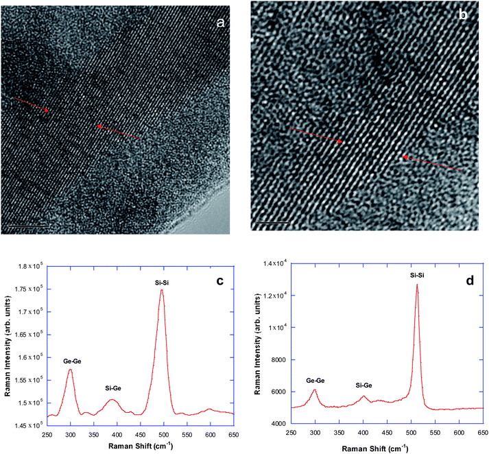
| Fig. 3 (a) HRTEM image of “sandwich” structure Er3+-doped SiGe NWs annealed at 600 °C for 1 h (scale bar = 5 nm); (b) Raman spectrum of the NWs annealed at 600 °C in N2 for 1 h; (c) Raman spectrum of the NWs annealed at 700 °C in N2 for 1 h. | ||
The samples were annealed at 600 °C or 700 °C in N2 for 1 h. The evolution of crystallinity can be probed by Raman spectroscopy. Previous studies on crystalline random Si1−xGex systems report the peak position of the Ge–Ge mode shifts linearly from 281 cm−1 to 300 cm−1 with increasing Ge mole fraction x,20 a shift of the Si–Si Raman-active mode decreasing from 521 cm−1 to 453 cm−1; and a strongly non-linear composition dependence of the corresponding Si–Ge peak position.21
More recent work on Raman analyses of SiGe nanowires have noted a similar compositional dependence of these modes, characterizing samples whose Ge fraction x varies from 0.12 to 0.95.22
The Raman spectrum obtained from a sample annealed at 600 °C (Fig. 3b) has a strong peak at 295 cm−1, attributed to scattering associated with Ge–Ge vibrations. There are two other very weak broad peaks appearing at 387 cm−1 and 494 cm−1, which are assigned to the scattering of the Si–Ge and Si–Si vibrations, respectively. Upon annealing at 700 °C, the Ge–Ge peak remains at 295 cm−1 but the Ge–Si and Si–Si peaks become sharper and shift to 392 cm−1 and 483 cm−1 respectively (Fig. 3c). Comparisons based principally on peak position of the Ge–Ge vibration with those reported earlier for the SiGe nanowires suggest a Ge-rich composition (>0.80), consistent with the HRTEM analysis and the fact that we begin with a Ge core nanowire as the first step in their fabrication. The intensities of the Si–Ge and Si–Si peaks also increase as a result of higher temperature annealing that is helpful in relaxing strain and improving crystallinity in the sample.23
 | ||
| Fig. 4 (a) SEM image of “Er-surface enriched” SiGe NWs; (b) EDX spectrum of the NWs; (c) TEM image of a typical NW (scale bar = 20 nm); (d) EDX linescans of the NW shown in the inset suggest that an average loading of ∼6% Er3+ is present in the center of the NWs (scale bar = 20 nm). | ||
 | ||
| Fig. 5 (a) HRTEM image of a “Er-surface enriched” SiGe NW (scale bar = 5 nm); (b) HRTEM image of another NW (scale bar = 2 nm); (c) Raman spectrum of the NWs after annealing in N2 at 600 °C; (d) Raman spectrum of the NWs after annealed in N2 at 700 °C. | ||
Fig. 5c and d are Raman spectra measured from this type of nanowire sample annealed at 600 °C and 700 °C in N2, respectively. For the sample annealed at 600 °C, Ge–Ge, Si–Ge, and Si–Si peaks appear at 301, 394, and 497 cm−1, respectively, whereas the Si–Ge Raman shift of the NWs annealed at 700 °C appears at 407 cm−1 and all features possess a relatively narrower linewidth after heating. The relative progression of increasing mode intensity with increasing Raman frequency is consistent with enhanced Si content in the alloy.22 It is again reasonable to expect that a higher temperature is beneficial to forming an alloy between Si and Ge, and due to the lack of Er impurity barrier inserted between the Si shell and the Ge core in the case of ‘sandwich’ NWs, more Si can diffuse into Ge core matrix to form alloys with higher concentration of Si for this type of NW. The increased intensity of Raman bands for the NWs annealed at 700 °C suggests that a more highly crystalline SiGe alloy is formed in this case.
 | ||
| Fig. 6 (a) SEM image of the “Co-deposited Er & Si” Ge core NWs; (b) EDX spectrum of the NWs shows the concentration of Er & Si is higher than that of “sandwich” NW under similar preparation conditions; (c) TEM image of the NWs; (d) EDX linescans of the NW shown in the inset indicate that the NW has a Ge-rich core and a Si & Er rich shell. | ||
 | ||
| Fig. 7 (a) Elemental maps of a single “Co-deposited Si & Er” NW (scale bars (top) are 25 nm for each); (b) HRTEM of the NW surface. Two regions are identified: area 1(majority), with a lattice constant of 3.19 Å (corresponding to (111) orientation Si0.45Ge0.55); area 2 (random) with a lattice constant of 2.79 Å close to that of (321) orientation cubic Er2O3 (2.82 Å); (c) Raman spectrum of the “Co-deposited Si & Er” Ge core NWs. | ||
For this type of sample, the extent of alloying is very sensitive to annealing temperature, as reflected in analysis by Raman spectroscopy. For the sample annealed at 600 °C in N2, only the Ge–Ge phonon scattering peak at 294 cm−1 is obtained, inferring that the SiGe phase is either amorphous or not formed at all under these conditions. This is in stark contrast to NWs annealed at 700 °C in N2 (Fig. 7c) demonstrating a broad peak ranging from 280 cm−1 to 400 cm−1; such a feature presumably originates from the heterogeneous Si1−xGex alloy with broad distribution of x values caused by this co-deposition fabrication method. In addition, there also appears to be a weak Si–Si phonon peak present at ∼517 cm−1.
The impact of NW structure and post-fabrication annealing on the near IR light emission
The structure of a given NW greatly affects the light emission intensity at 1.54 µm (Fig. 8), which originates from the intra-f-shell transition associated with the 4I13/2 → 4I15/2 levels in the Er3+ centers. Overall, the strongest light emission from Er3+ in these types of SiGe NWs is obtained from ‘Co-deposited Si & Er’ on a Ge core NW (Fig. 8a). ‘Sandwich’ structure Er3+-doped SiGe NWs have a modest emission intensity at 1540 nm after an appropriate annealing in N2, which is approximately 1/3 of the emission intensity from a similarly treated co-deposited NW (Fig. 8c). For the case of “Er-surface enriched” SiGe NWs (Fig. 8e), negligible light emission in the near IR is obtained, except in the cases of samples coated with a very thin silicon surface layer (∼50 nm) and annealed in air instead of nitrogen; such samples yield much stronger near infrared light emission (Fig. 8b). The light emission for Er-doped Ge NWs is shown in Fig. 8d for comparison; note that its intensity is, under comparable excitation conditions, weaker than all SiGe-containing systems—with the exception of the erbium surface-enriched SiGe nanowire sample. | ||
| Fig. 8 Room temperature photoluminescence (PL) spectra of all types of NWs. (a) PL of “Co-deposited Si & Er” Ge core NW annealed in N2 at 600 °C; (b) PL of “Er-surface enriched” SiGe Structure NW annealed in air at 600 °C; (c) PL of “sandwich” structure NW annealed in N2 at 600 °C; (d) PL of Er-doped Ge NW annealed in air at 600 °C; (e) PL of “Er-surface enriched” SiGe Structure NW annealed in N2 at 600 °C (λex = 488 nm at 200 mW). | ||
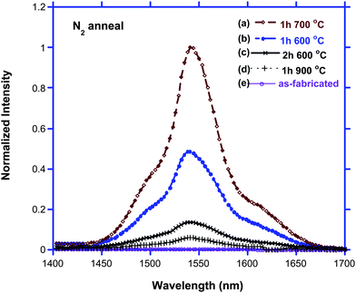 | ||
| Fig. 9 PL spectra of “Co-deposited Si & Er” Ge core NWs. (a) PL of 1 h Si & Er co-deposition NW annealed in N2 at 700 °C for 1 h; (b) PL of 1 h Si & Er co-deposited Ge NW annealed in N2 at 600 °C for 1 h; (c) PL of 2 h co-deposited NW annealed in N2 at 600 °C for 1 h; (d) PL of as-fabricated NW (λex = 488 nm at 200 mW). | ||
Preliminary experiments also suggest that there is a reactant concentration dependence to the intensity of light emission observed for these types of structures. The magnitude of near IR PL also decreases if the co-deposition duration of Si and Er is extended from 1 h to 2 h (Fig. 9c), likely a consequence of more extensive self-quenching from the additional Er3+ ions present, along with a greater Si to Ge ratio in the annealed NWs. The former phenomenon is quite common for erbium, while the latter is in agreement with literature report that erbium-doped SiGe films with higher Ge content grown by molecular beam epitaxy (MBE) are less strained, resulting in a stronger PL intensity.24,25
In an attempt to locate where the optically active Er3+ ions are present, a buffered HF solution was employed. In this case, the etch addresses two possibilities: (1) if the emitting Er3+ centers are localized in an oxide-rich environment at the surface, such ions will be removed; (2) given literature precedents for enhanced dissolution reactivity of Si NWs in HF solutions,26 it is also likely that erbium ions residing in a polycrystalline structural environment on the nanowire shell will also be removed by this etch. Thus, when these ‘Co-deposited’ NWs are exposed to a buffered HF solution, their color becomes darker due to the removal of the light-contrast oxide shell after etching. The light emission at 1.54 µm vanishes completely, which suggests that the optically active Er centers lie inside the shell where higher concentrations of both Er and Si are located.
To further understand the underlying mechanism for the observed 1.54 µm photoluminescence, photoluminescence excitation (PLE) measurements were carried out. Although a slight enhancement of Er-related PL was observed using a 488 nm laser excitation, no distinct increase of the Er-related PL was found upon excitation at 514 nm (Fig. 12a). It can be thus inferred that a carrier-mediated process dominates the process of producing light emission at 1.54 µm.9 A typical UV/visible absorption spectrum of “Co-deposited Si & Er” Ge core NW dispersed in ethylene glycol reveals a broad absorption tail ranging from 300 nm to 600 nm (ESI†).
 | ||
| Fig. 10 PL spectra of “sandwich” structure Er-doped SiGe NW. (a) PL spectrum of the NW annealed at 600 °C in N2 for 1 h; (b) PL spectrum of the NW annealed at 700 °C in N2 for 1 h; (c) PL spectrum of the NW with 0.5 h Er deposition time annealed 600 °C in N2 for 1 h; (d) PL spectrum of the as-fabricated NW (λex = 488 nm at 300 mW). | ||
In a manner quite different from the ‘Co-deposited Si & Er’ NWs, the PL intensity of ‘sandwich’ NWs is significantly increased upon excitation at both 488 and 514 nm (Fig. 12c), which implies that direct excitation mechanism is responsible for the luminescence at 1.54 µm. A typical UV/visible absorption spectrum of ‘sandwich’ structure Er-doped SiGe NWs reveals a broad absorption tail extending beyond the visible light range (ESI†).
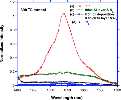 | ||
| Fig. 11 Photoluminescence (PL) spectra of “Er-surface enriched” SiGe NW. (a) PL spectrum of the NW annealed in air at 600 °C. (b) PL spectrum of the NW with thicker Si coating and annealed in N2 at 600 °C. (c) PL spectrum of the NW with thicker Si coating and shorter (0.5 h) Er deposition time that was annealed in N2 at 600 °C. (d) PL spectrum of the NW annealed in N2 at 600 °C. | ||
‘Er-surface enriched’ SiGe NWs with relative high concentrations of Ge were also fabricated by reducing the exposure time of SiH4 to the Ge NW core. Similar to the NW with high concentrations of Si, these ‘Er-surface enriched’ NWs with a correspondingly higher concentration of Ge has no emission after annealed in N2 at 600 °C and very weak emission after being annealed at 700 °C (Fig. 11d). Changing the nature of the gaseous ambient to air results in enhancement of the PL intensity of the NW by more than one order of magnitude (Fig. 11a). This is a consequence of several synergistic factors. First, a thinner Si coating presumably facilitates the diffusion of Ge out into the Si layer, and after oxidation in air, GeOx (or perhaps SiGeOx) with tunable band gap can form and assist in enhancing the PL performance through a carrier-mediated process.28 It should also be noted that the co-doping of oxygen and erbium into crystalline Si greatly increases the amount of excitable Er ions and reduces the room temperature quenching process.29
The PLE behavior of ‘Er-surface enriched’ SiGe NWs annealed in N2 shows an enhanced emission intensity for 488 nm excitation relative to 476 nm, but with an overall diminution in PL intensity with the remaining wavelengths out to 514 nm (Fig. 12b). This suggests that both carrier-mediated and direct excitation processes determine the light emission intensity of this type of NW structure.
 | ||
| Fig. 12 Excitation wavelength dependence of (a) “Co-deposited Si & Er” Ge NW; (b) “Er-surface enriched” SiGe NW; and (c) “sandwich” structure Er-doped SiGe NW. | ||
Discussion
‘Sandwich’ structure
In this type of sample, HRTEM lattice imaging, Raman analyses, and EDX linescans point to an alloy structure that is clearly Ge-rich at the core, with some Si present (∼10%). Hence, the presence of the Er3+ at the interface between Si and Ge does not inhibit Si diffusion into the core with annealing; however, the EDX data suggest that the energy barrier for Er diffusion is significantly lower into the Ge layer than outward into the Si-rich surface layer. A clear compositional gradient does exist, as the surface cap appears amorphous and oxygen rich, with a total absence of erbium. With particular regard to the erbium, the largest concentration of centers is localized at the boundary between the SiGe core and the Si oxide shell.While it is possible with this type of geometry to achieve an emissive Er3+ environment, this relatively high concentration of rare earth ions at the boundary (∼6%) is at a level capable of self-quenching. The weaker 1.54 µm PL of this system (with respect to the two other configurations studied here) is consistent with this conclusion. Detectable emission, when activated by a necessary 600 °C anneal does follow an excitation pathway that involves direct excitation of the Er3+ ligand field levels associated with the 4I15/2 → 4G7/2 and 4I15/2 → 4H9/2 transitions, and not excitons originating from the SiGe phase. Extended anneals at higher temperatures (700 °C) result in a corresponding drop in emission intensity at 1.54 µm, likely only serving to facilitate clustering of erbium centers in this type of sample.
Erbium-surface rich structure
The lack of a diffusion barrier between Ge and Si layers is presumed to facilitate intermixing of the two elements during annealing at 700 °C, and the comparable levels of each element present in the core are consistent with this conclusion.Not surprisingly, this deposition sequence produces the greatest concentration of erbium at the outermost surface of the nanowire, and thus greater opportunities for clustering. This significant erbium fraction present at the surface is structurally reminiscent of the previously studied Er-surface enriched Si nanowires, where a relatively high erbium fraction (>20%) and very weak near IR emission is observed.13
Not surprisingly, the emission intensity at 1.54 µm of these ‘Er-surface enriched’ SiGe NWs is quite weak when annealed in N2 at 600 °C (Fig. 12b); the corresponding UV/visible absorption spectrum of this type of sample shows a weak absorption cross-section (ESI†), which diminishes the possibility of carrier-mediated excitation processes in the erbium photoluminescence. For these NWs annealed in air, the greater PL emission intensity at 1.54 µm likely originates with the dominance of direct excitation of the rare earth ligand field states, as noted for the ‘sandwich’ architecture described above.
Erbium–silicon Co-deposited structure
The structure of this type of nanowire, especially at the surface, is rather different than the two other varieties described in this paper. HRTEM analyses suggest a coating of Si randomly oriented nanocrystals that presumably ‘break up’ the erbium–erbium clustering present in the Er-surface enriched and sandwich nanowire structures. While simultaneous deposition of erbium and silicon onto the Ge NW core likely reduces opportunities for radial epitaxial growth, it nevertheless permits relatively higher fractions of optically active rare earth to be introduced into this type of nanowire. Significant Si diffusion into the Ge core, and subsequent alloying, also takes place upon annealing.Post-fabrication annealing can introduce oxygen impurities that assist in the formation of a non-centrosymmetric coordination environment for Er ions, necessary for yielding much stronger light emission.30 Hence activation by heating at 600 or 700 °C is necessary in these samples; yet use of temperatures higher than these (e.g. 900 °C) results in a significantly diminished PL signal at 1.54 µm, which is associated with a clustering of erbium ions at temperatures closer to the recrystallization temperature of silicon (and an upper thermal threshold for PL activation).
In addition to relative PL intensity at 1.54 µm, analysis of the emission intensity dependence on excitation wavelength finds an overall diminution with increasing excitation wavelength, consistent with carrier-mediated behavior. Strong absorption by this type of sample well into the visible region (>600 nm, detected by electronic absorption) is consistent with this conclusion as well.
Overall, based on the fabrication method the local erbium coordination environment found in this ‘co-deposited’ sample is presumed to resemble that found in erbium-doped silicon-rich silicon oxide films produced by CVD, co-sputtering, and related methods. It is structures of this type that are showing promise in reported observations of optical gain, and we believe that this architecture may ideally prove useful in electroluminescent structures involving carrier transport through a Ge core NW with desirable carrier mobilities. In order to properly elucidate mechanistic details for the near IR PL of these SiGe NWs, more detailed photophysical investigations are desired.
Summary
The studies presented in this work are a clear example of how the relative timing of introducing a dopant or impurity center during semiconductor nanowire fabrication can alter element inter-diffusion during subsequent thermal treatment as well as the clustering of the optically active impurity centers.Further efforts are required to both fully understand the photoluminescence mechanism of these three types of NWs and improve the efficiency of each. Preliminary studies outlined here suggest the necessity of diluting the amount of either erbium or silicon in the structure when such elements are localized along the nanowire shell. As a next generation architecture, multilayer Er-doped SiGe NWs with greatly reduced thicknesses of both Si and Er, which will drastically reduce the diffusion barrier, should produce improved emissive character; these experiments, along with a careful analysis of near IR emission intensity and excitation cross-section of these samples relative to known emissive erbium-doped semiconducting systems, are a part of significant future studies.
Experimental
Er3+-doped SiGe NWs synthesis
To describe briefly, a mixture of carbon (J. T. Baker, reagent grade) and germanium powder (Strem, 99.999%) with a C/Ge molar ratio of 3![[thin space (1/6-em)]](https://www.rsc.org/images/entities/char_2009.gif) :1 was loaded into an alumina boat and then placed in a quartz tube reactor. A 5 × 8 mm2 piece of a Si wafer covered with a 12 nm thermally evaporated Au film was placed in another alumina boat that was positioned 3 cm from the edge of the oven. The ceramic oven (30 cm in length) was heated at 850 °C for 2 h, and then at 1000 °C for 1.5 h under a 3000 sccm helium (Praxair, UHP grade) flow. Upon completion of the reaction, a thick brown fluffy film can be easily seen on the wafer. The average yield of the Ge NWs is about 0.3 mg. In all experiments involving Si and Er deposition, the Ge nanowires must be used immediately for the next fabrication step to avoid surface oxidation, which will result in nanowire surfaces with rough morphologies.
:1 was loaded into an alumina boat and then placed in a quartz tube reactor. A 5 × 8 mm2 piece of a Si wafer covered with a 12 nm thermally evaporated Au film was placed in another alumina boat that was positioned 3 cm from the edge of the oven. The ceramic oven (30 cm in length) was heated at 850 °C for 2 h, and then at 1000 °C for 1.5 h under a 3000 sccm helium (Praxair, UHP grade) flow. Upon completion of the reaction, a thick brown fluffy film can be easily seen on the wafer. The average yield of the Ge NWs is about 0.3 mg. In all experiments involving Si and Er deposition, the Ge nanowires must be used immediately for the next fabrication step to avoid surface oxidation, which will result in nanowire surfaces with rough morphologies.
In the second step, three different permutations involving deposition of Er3+ and Si on the Ge core NWs were employed, as described above. The Si atoms were obtained via the pyrolysis at 500 °C of 0.5% silane diluted in helium (Voltaix) flowing at 4.0 sccm and further diluted by 3000 sccm helium (Praxair, UHP grade). The Er3+ atoms were obtained from Er(tmhd)3 (Strem) vapor. Er(tmhd)3 was heated to 145 °C in a bubbler, and its vapor was carried downstream by 3000 sccm of helium (Praxair, UHP grade) to the pyrolysis oven operating at 500 °C.
The resulting Si/Er coated Ge NW were annealed in a N2 atmosphere. In selected experiments, Buffered-HF Improved (Transene, AR grade) was employed to etch away the oxide shell of the Route 1 NWs. The etching time is 5 minutes, and the etched NWs were rinsed with 2-propanol for several times and dried in air before measuring their photoluminescence.
Characterization
Structural characterization of all samples was performed using a JEOL JEM-2010F field emission transmission electron microscope (TEM) at the University of Illinois-Chicago. The TEM operates both in transmission and scanning transmission modes. A probe size of 1 nm was used for both point analysis and EDX linescan across the nanowires. Specimens for TEM characterization were prepared by dispersing the sample with a 10 µL drop of 2-propanol and then placing the drop onto a grid. EDX analyses of macroscopic nanowire samples were performed using a JEOL JSM-6100 SEM at Texas Christian University. Low resolution (±4 nm) near-IR photoluminescence (PL) spectra were obtained using an Applied Detector Corp. liquid N2-cooled Ge detector using a standard in-phase technique Stanford Research Systems Chopper/Lock-in amplifier. Excitation was provided by a Coherent Ar+ laser. Emitted light was collected at a 40° angle relative to the excitation direction. It was filtered by a RG1000 filter (Melles Griot) and dispersed by an Acton Research Corp. 0.25 m monochromator.Raman spectra were recorded using a standard Raman micro-imaging system. Excitation was provided by the 514 nm line of an argon ion laser. The sample was mounted onto a computer controlled X–Y–Z stage. The system with a CCD detector had 4.0 cm−1 resolution. An Olympus BH-2 microscope with a 100× objective allowed the collection of scattered light from spots as small as 1 µm.
Acknowledgements
We gratefully acknowledge support for this research by the Robert A. Welch Foundation (Grant P-1212). The expertise of Dr Alan Nichols of the Electron Microscopy Facility of the Research Resources Center of the University of Illinois-Chicago is also greatly appreciated. Useful discussions with Professor Leandro Tessler of UNICAMP are gratefully acknowledged.References
- G. Dehlinger, L. Diehl, U. Gennser, H. Sigg, J. Faist, K. Ensslin, D. Grutzmacher and E. Muller, Science, 2000, 290, 2277 CrossRef CAS.
- M. Myronov, C. P. Parry, O. A. Mironov and E. H. C. Parker, Appl. Phys. Lett., 2004, 85, 3145 CrossRef CAS.
- A. T. Naveed, J. H. Evans-Freeman, K. D. Vernon-Parry, A. C. Wright, D. C. Houghton and A. R. Peaker, Semicond. Sci. Technol., 2000, 15, 91 CrossRef CAS.
- M. Telford, III-Vs Review, 2004, 17, 32 Search PubMed.
- A. Borak, Science, 2005, 308, 638 CrossRef CAS.
- S. A. Lynch, R. Bates, D. J. Paul, D. J. Norris, A. G. Cullis, Z. Ikonic, R. W. Kelsall, P. Harrison, D. D. Arnone and C. R. Pidgeon, Appl. Phys. Lett., 2002, 81, 1543 CrossRef CAS.
- M. L. Lee and E. A. Fitzgerald, J. Appl. Phys., 2005, 97, 011101-1.
- C. M. Lieber, MRS Bull., 2003, 28, 486 CAS.
- J. St. John, J. L. Coffer, Y. Chen and R. F. Pinizzotto, J. Am. Chem. Soc., 1999, 121, 1888 CrossRef CAS.
- R. A. Senter, Y. Chen and J. L. Coffer, Nano Lett., 2001, 1, 383 CrossRef CAS.
- J. St. John, J. Coffer, Y. Chen and R. Pinizzotto, Appl. Phys. Lett., 2000, 77, 1635 CrossRef.
- J. Ji, R. Senter, L. R. Tessler, D. Back, C. H. Winter and J. L. Coffer, Nanotechnology, 2004, 15, 643 CrossRef CAS.
- Z. Wang and J. L. Coffer, Nano Lett., 2002, 2, 1303 CrossRef CAS.
- Z. Wang and J. L. Coffer, J. Phys. Chem. B, 2004, 108, 2497 CrossRef CAS.
- J. Wu, P. Punchaipetch, R. M. Wallace and J. L. Coffer, Adv. Mater., 2004, 16, 1444 CrossRef.
- T. Hanrath and B. A. Korgel, J. Am. Chem. Soc., 2004, 126, 15466 CrossRef CAS.
- J. D. Carey, R. C. Barklie, J. F. Donegan, F. Priolo, G. Franzo and S. Coffa, J. Lumin., 1998, 80, 297 CrossRef CAS.
- A. Kenyon, Semicond. Sci. Technol., 2005, 20, R65–R84 CrossRef CAS.
- S. Ossicini, L. Pavesi and F. Priolo, Light Emitting Silicon for Microphotonics (Springer Tracts in Modern Physics), Springer, Berlin, 2003, vol. 194, p. 182 Search PubMed.
- H. K. Shin, D. J. Lockwood and J. M. Baribeau, Solid State Commun., 2000, 114, 505 CrossRef CAS.
- W. J. Brya, Solid State Commun., 1973, 12, 253 CrossRef CAS.
- Q. Lu, K. Adu, H. Gutiérrez, G. Chen, K.-K. Lew, P. Nimmatoori, X. Zhang, E. C. Dickey, J. Redwing and P. C. Eklund, J. Phys. Chem. C, 2008, 112(9), 3209 CrossRef CAS.
- W. K. Choi, L. K. Teh, L. K. Bera, W. K. Chim, A. T. S. Wee and Y. X. Jie, J. Appl. Phys., 2002, 91, 444 CrossRef CAS.
- H. Yin, R. L. Peterson, K. D. Hobart, S. R. Shieh, T. S. Duffy and J. C. Sturm, Mater. Res. Soc. Symp. Proc., 2003, 765, D4.7.1.
- L. V. Krasil'nikova, M. V. Stepikhova, Yu. N. Drozdov, M. N. Drozdov, Z. F. Krasil'nik, V. G. Shengurov, V. Yu. Chalkov, S. P. Svetlov and O. B. Gusev, Phys. Solid State, 2005, 47, 93 CrossRef CAS.
- B. K. Teo, W. W. Chen, X. H. Sun, S. D. Wang and S. T. Lee, J. Phys. Chem. B, 2005, 109, 21716 CrossRef CAS.
- A. Polman and F. C. J. M. van Veggel, J. Opt. Soc. Am. B, 2004, 21, 871 Search PubMed.
- J. H. Chen, D. Pang, H. M. Cheong, P. Wickboldt and W. Paul, Appl. Phys. Lett., 1995, 67, 2182 CrossRef CAS.
- S. Coffa, G. Franzo, F. Priolo, A. Polman and R. Serna, Phys. Rev. B: Condens. Matter, 1994, 49, 16313 CrossRef CAS.
- F. Priolo, G. Franzo, S. Coffa, A. Polman, S. Libertino, R. Barklie and D. Carey, J. Appl. Phys., 1995, 78, 3874 CrossRef CAS.
Footnote |
| † Electronic supplementary information (ESI) available: additional EDX data of the erbium-doped SiGe nanowires; UV/Visible absorption spectra for the different SiGe nanowire configurations. See DOI: 10.1039/c0nr00476f |
| This journal is © The Royal Society of Chemistry 2010 |