Ordered arrays of shape tunable CuInS2 nanostructures, from nanotubes to nano test tubes and nanowires
Liang
Shi
*a,
Congjian
Pei
b and
Quan
Li
b
aDepartment of Chemistry, University of Science and Technology of China, Hefei, 230026, P. R. China. E-mail: sliang@ustc.edu.cn; Fax: +86-551-3607402; Tel: +86-551-3607234
bDepartment of Physics, The Chinese University of Hong Kong, Shatin, New Territory, Hong Kong, P. R. China
First published on 8th September 2010
Abstract
Well-aligned arrays of chalcopyrite CuInS2 one dimensional nanostructures have been prepared in a controllable manner via a convenient wet-chemical approach using anodic aluminium oxide (AAO) as a hard template. Highly oriented CuInS2 nanotubes, nano test tubes and nanowires arrays can be selectively grown by simply varying reaction conditions. Oleylamine (OLA) was found to play a key role in the synthesis and morphology control of the CuInS2 product. The structure, morphology, composition and optical absorption properties of the as-prepared samples were characterized using X-ray powder diffraction, transmission electron microscopy, energy dispersive X-ray spectrometry, scanning electron microscopy and UV–Vis spectrophotometry. The formation mechanism of the CuInS2 arrays is discussed.
1. Introduction
As an important ternary I-III-VI2 chalcopyrite semiconductor, CuInS2 has attracted much attention recently for its various excellent optical and electrical properties. It is well-known that CuInS2 has a high absorption coefficient and its band gap (1.5 eV) matches the desired absorption range of the solar spectrum.1 CuInS2 has also good structural defect tolerance, low toxicity and easy conversion of n/p carrier type.2,3 Synthesis and properties of nanostructured I-III-VI2 chalcopyrite materials including CuInS2 have been actively studied because the shape and size of these nanoscale semiconductors may exert a significant influence on their optoelectronic function and device performance, and sometimes induce unique physical and chemical properties different from their bulk counterparts. Some novel features have been found in the nanoscale semiconductor systems, such as an obvious enhancement of solar energy conversion efficiencies of photovoltaic devices covered with nanocrystalline-based semiconductor absorber layers.4,5Various morphologies of CuInS2 nanostructures including nanorods, nanoacorns, nanobottles, hollow nanospheres, foam-like and flower vase-like nanoparticles have been prepared by diverse methods.6–9 However, the preparation of CuInS2 arrays with well-aligned one dimensional (1D) nanostructures has seldom been reported.10 The fabrication of arrays with well-aligned 1D semiconductor nanostructures (nanowire, nanotube or nanorod) with intensified anisotropy are highly desirable because it is a key step toward building functional nanodevices such as nanoscale electronics and molecular sensors. To date, it remains a challenge to control the preparation of large scale 1D nanostructured CuInS2 arrays with desired shapes. The template method is one of the most efficient methods for the fabrication of highly ordered well-distributed one-dimensional nanomaterials, especially for nanotubes and nanowires.11,12 Among various types of templates, porous anodic aluminium oxide (AAO) is a particularly effective hard template, due to its advantages including monodisperse size distribution, high pore density, nearly parallel porous structures and easily controlled pore diameter.13–15 Most importantly, AAO templates are thermally and mechanically stable; hence they can be employed in more rigorous reaction conditions. Here we report a convenient solution approach with porous alumina templates as hard templates for preparation of CuInS2 arrays of well-aligned one dimensional nanostructures. Moreover, the fabrication of CuInS2 nanotubes, nano test tubes and nanowires arrays was controlled by simply varying the reaction conditions.
2. Experimental section
All reagents are analytical grade and used without further purification. Copper(II) acetylacetonate (Cu(acac)2), indium(III) acetylacetonate (In(acac)3), elemental sulfur, o-dichlorobenzene (DCB) and oleylamine (OLA) were used as starting materials. AAO templates (Whatman Co., U.K.) with pore sizes of 200 nm in diameter were used in the experiments.In a typical procedure, for the fabrication of CuInS2 nanotube array within the AAO template, 1 mmol copper(II) acetylacetonate (Cu(acac)2), 1 mmol indium(III) acetylacetonate (In(acac)3) and 2 mmol elemental sulfur were added to a 25 mL three-neck flask in air. Then 10 mL DCB and 4 mL OLA were added into the above flask with mild magnetic stirring. Afterward, an AAO template was added into the flask and immersed in the liquid. The above liquid mixture in the flask was treated by sonication for 5 min to remove air in the pore of AAO template and fill the pore with liquid. The flask was attached to a Schlenk line and purged of oxygen and water under vacuum for 30 min, followed by nitrogen bubbling for 30 min with mild magnetic stirring. The evacuation and N2 bubbling process was cycled for 3 times at room temperature. The flask was then heated to 100 °C, maintaining a N2 flow. The evacuation and nitrogen bubbling process was conducted at 100 °C again once. The sonication, multi-evacuation and bubbling process was important to enhance the filling efficiency of the AAO template pores with the mixture of reaction solution. Subsequently, a uniform and high density of as-synthesized sample can be obtained. The reaction mixture is refluxed at about 180 °C for 1 h under N2 flow. The reaction was allowed to cool to room temperature and the AAO template containing the product was taken out from the flask, thoroughly washed with ethanol and distilled water, and dried in air. For the fabrication of the CuInS2 nanowire array, the amount of OLA is decreased to 2 mL and other procedures remained the same.
The overall crystallinity of the product is examined by X-ray diffraction (XRD, Rigakau RU-300 with Cu-Kα radiation). The general morphology of the products was characterized using scanning electron microscopy (FESEM QF400). Detailed microstructure analysis was carried using transmission electron microscopy (TEM Tecnai 20ST). The chemical composition analysis was obtained by energy dispersive X-ray spectrometry (EDX) using an EDX spectrometer attached to the same microscope. For the SEM measurements, several drops of 1 M NaOH aqueous solution were added onto the sample to dissolve some part of the AAO template. The residual solution on the surface of the template was rinsed with distilled water. For the TEM and HRTEM measurements, the template was completely dissolved in 2M NaOH aqueous solution. The product was centrifuged, thoroughly washed with distilled water to remove residual NaOH and then rinsed with absolute ethanol.
3. Results and discussion
The crystal structure of the product was firstly characterized by X-ray diffraction (XRD) to obtain information on crystal structure and phase composition. A typical XRD pattern of the as-prepared CuInS2 product is shown in Fig. 1. All diffraction peaks can be indexed to the chalcopyrite (tetragonal) structured CuInS2. After refinement, the lattice constant, a = 5.524 Å and c = 11.137 Å, is obtained, which matches well to the reported value for CuInS2 crystal (JCPDS card, No. 85-1575). The broadening of the XRD peaks suggests that the grain sizes of the product are on a nanometre scale. No other phases are found in the product. XRD pattern shows an increasing background at small diffraction angles, this originates from the diffraction of amorphous alumina in the AAO hard template.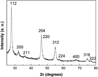 | ||
| Fig. 1 A representative XRD pattern of the as-prepared CuInS2 nanostructures. | ||
The product obtained from the reaction conducted with 4 mL OLA was characterized by SEM. Fig. 2a shows an image of sample with the template partially removed. It can be seen clearly that a large-scale array of highly ordered dense nanotubes protrude from the inner surface of the AAO template pores. These nanotubes are all straight and parallel to each other and oriented vertically to the surface of the AAO template. The size distribution of the as-prepared nanotubes is uniform over the entire area and the average diameter of the nanotubes is about 200 nm, which is consistent with the pore size dimension of the AAO template. The wall thickness of the nanotubes is about 20 nm. It is also found that some isolated nanotubes originating from the breaking of long nanotubes lie on the top of the array, in which case a through-length hollow characteristic can be observed. The CuInS2 nanotubes are structurally robust—although the AAO template has been partially removed, the array configuration remains without collapse. In addition, due to the partial removal of the template, the remnant part should give some extra strength for these nanotubes to support themselves. This make the formed nanotubes array more structurally stable than the corresponding arrays without any such mechanical support. The well-aligned nanotube CuInS2 array may produce ordered p-n junctions and continuous charge carrier transport pathways without dead ends, which may bring about an even higher efficiency of solar cells. Detailed microstructure information and chemical composition of individual nanotube are obtained from TEM related studies including imaging, selected area electron diffraction (SAED) and energy dispersive X-ray spectrometry (EDX). A typical TEM image of a nanotube is shown in Fig. 2b, which confirms that the nanotubes have a uniform diameter of 200 nm and their surface is smooth. The dark/light/dark contrast along the radial direction gives evidence of its hollow tube structure. The diffraction rings in the SAED pattern product taken from such an nanotube, as displayed in the inset of Fig. 2b, reveals its polycrystalline nature. The diffraction ring with the strongest intensity can be indexed to the (112) pane, which may be induced by a preferred growth orientation. The EDX spectrum (Fig. 2c) from the product shows intense peaks of Cu, In and S, displaying the composition as Cu, In and S only. The gold and carbon signals come from the supporting TEM grid. EDX quantitative analysis gives an average Cu/In/S composition ratio of 1![[thin space (1/6-em)]](https://www.rsc.org/images/entities/char_2009.gif) :1:2, in accordance with the stoichiometry of CuInS2. A HRTEM image (Fig. 2d) shows that the as-prepared nanotubes consist of small nanocrystalline domains, displaying their polycrystalline structure. The lattice spacing of most of these CuInS2 single-crystalline particles can be ascribed to the (112) planes of chalcopyrite CuInS2, suggesting similar alignment direction, which is in agreement with the SAED image.
:1:2, in accordance with the stoichiometry of CuInS2. A HRTEM image (Fig. 2d) shows that the as-prepared nanotubes consist of small nanocrystalline domains, displaying their polycrystalline structure. The lattice spacing of most of these CuInS2 single-crystalline particles can be ascribed to the (112) planes of chalcopyrite CuInS2, suggesting similar alignment direction, which is in agreement with the SAED image.
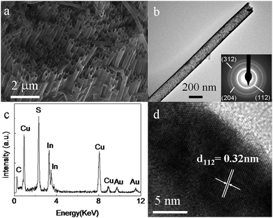 | ||
| Fig. 2 SEM (a), TEM (b), SAED (inset of b) and HRTEM (d) images and EDX spectrum(c) of the as-prepared CuInS2 nanotubes array. | ||
Fig. 3 shows the room temperature UV–Vis absorbance spectrum for the as prepared CuInS2 nanotube sample. Strong photo absorption occurs in the entire visible region, giving rise to the black color of the sample. The as prepared CuInS2 nanotube array should be an effective photocatalyst for solar-driven applications due to its high absorption to the visible light. Estimates of the optical band gap engrgy (Eg) can be obtained using a curve of (αhν)2versus photon energy plotted in the inset of Fig. 3, here α is the absorption coefficient, h is Planck's constant, and ν is frequency. The Eg value is calculated to be 1.76 eV based on the intersection of the extrapolated linear portion, being higher than that of bulk CuInS2 (1.53 eV),16 arising from the quantum size effects from the nanometre sized CuInS2 grains in the polycrystalline nanotube.
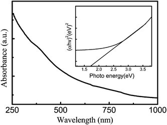 | ||
| Fig. 3 A typical room-temperature UV–visible absorbance spectrum of the as-prepared CuInS2 nanotubes and the bandgap value (inset: estimation of (αhν)2versus photon energy plotted by a curve). | ||
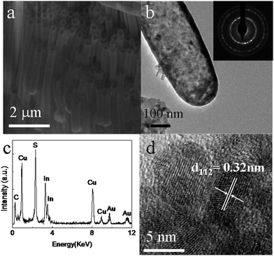
It is found that the amount of OLA has a significant influence on the morphology of the CuInS2 product. If the amount of OLA is decreased to 2 ml with other reaction conditions unchanged, a nanowire array, instead of nanotube array, can be obtained. Fig. 4a shows a SEM image of the as-prepared sample with the template partially removed. One can see that highly ordered array of uniformly distributed nanowires are grown in a large area. These nanowires are continuous, smooth and parallelly aligned. A TEM image in Fig. 4b indicates that the as-prepared nanowires are clean, straight and have a diameter of about 200 nm. SAED pattern (inset of the Fig. 4b) shows diffraction rings, disclosing the polycrystalline nature of the CuInS2 nanowires. The EDX spectrum in Fig. 4c shows its chemical composition of only Cu, In and S only with an atomic ratio of 1:1:2. A HRTEM image (Fig. 4d) shows crystalline domains and confirm nanowires are polycrystalline. The clear lattice spacing of 0.32 nm of one domain in the HRTEM can be indexed to (112) planes of chalcopyrite (tetragonal) CuInS2.
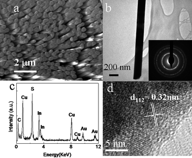 | ||
| Fig. 4 SEM (a), TEM (b) and SAED (inset of b) and HRTEM (d) images and EDX spectrum(c) of the as-prepared CuInS2 nanowires array. | ||
A possible formation mechanism of CuInS2 nanotubes and nanowires arrays could be proposed here according to the experimental results. During the reaction process, AAO templates were first immersed in the reaction solution. The sonication and multi-cycles of evacuation and bubbling process ensure removal of gas from the AAO template pores, filling them with reaction solution by negative pressure and capillary effect. The experimental results indicated that oleylamine played a key role in the preparation of CuInS2. As an organic base, oleylamine provided a strong reductive environment and can decrease precursor decomposition temperature dramatically.17 Therefore, the oleylamine here acted as an activation agent expediting the precursor decomposition process. This will remove the reactivity difference of the precursors and the formation of the homogeneous ternary nanocrystals becomes favorable. When the temperature was increased during the reaction process, the sulfur was first reduced to S2− ions and the Cu and In precursors decomposed. It is well-known that the pore walls of AAO were positively charged due to the presence of a layer of acidic anions held either covalently or present as hydrated anions (complex anions Al(H2O)4(OH)+2 and Al(H2O)+4).18 Therefore, the S2− ions attached preferentially to the pore wall and then induced colloidal CuInS2 deposition on the pore wall owing to the electrostatic forces between the colloid and the AAO pore wall. For template aided synthesis, the nucleation and crystal growth were all confined to the pores of the template. In the nucleation stage, it is possible for either homogeneous nucleation or heterogeneous nucleation to occur in the solution.13 If the interactions between reagent molecules are stronger than those between the reagent molecules and the pore walls, homogeneous nucleation and crystal growth will happen within the voluminous pores near the center and solid single crystalline nanowires or nanorods will be formed as a result. On the contrary, heterogeneous nucleation and crystal growth on pore walls will happen if the interactions between the reagent molecules are weaker than those between the reagent molecules and the pore walls. In this case, heterogeneous nucleation on pore walls generally leads to polycrystalline materials in an AAO template aided synthesis. Furthermore, the crystal growth should start from the wall and the channels of the template confined the crystal-growth shape. During the initial crystal growth stage, one-dimensional polycrystalline nanotubes with diameter determined by the pore size in the AAO template will be generated. Since the crystal growth started from the inner surface of pore walls and extend to the center, the thickness of the nanotubes' wall would become thicker if the reaction proceeds all along. The AAO pore could be filled completely and form solid nanowires with the continuous lateral thickening finally.
In our present case, the product is polycrystalline nanotubes and colloidal CuInS2 deposition exists on the pore wall owing to the electrostatic forces between the colloid and the AAO pore wall. Therefore, in the reaction process, the heterogeneous nucleation on pore walls should happen at the initial stage and accompanied by crystal growth under confinement of the pore walls geometry. With the assembly of the as-formed particles, the final product would be of tubular structure with outer diameter determined by the pore diameter in the AAO template, which is in accordance with our product. On the other hand, OLA also served as an effective capping ligand19 which on binding to the nanocrystal surface further slowed down the growing process once the CuInS2 nucleated on the AAO inner surface. If the amount of OLA is decreased, the suppression on the nucleation and crystal growth will be less significant. The crystal growth can quickly extend to the center of the AAO pore once it starts from the inner surface of AAO pore walls. In such a manner, the AAO pore will be filled completely by continuously lateral thickening of the tubular structure. As a result, the nanowires will form within the pores.
Based on the above proposed mechanism for the nanotube array, it occurred to us that if we use a template where one end of the AAO pores are closed and the other ones are left open, we should obtain a CuInS2 array of nanotubes with one end closed and the other open, i.e. a nano test tube array configuration. We therefore conducted the experiment using the AAO template without removing the underlying aluminium, while other experimental conditions were kept the same. Fig. 5a illustrates a SEM image of the as-prepared sample with the template partially removed. The product is composed of an ordered nanotube array. Fig. 5b is a typical TEM image of the sample, disclosing, as expected, that the nanotubes have unambiguously closed round ends. The EDX (Fig. 5c) and HRTEM (Fig. 5d) results prove these nano test tubes are pure CuInS2 and with polycrystalline nature, similar to the nanotubes with both open ends. The as-prepared nano test tubes with only one end open may find their applications in the field of drug delivery carriers, nanoscale chemical reactors and energy storage media. It would be convenient to fill the nano test tubes with desired molecules. If chemistry is performed in these nano test tubes, nanoscale confinement effects should appear, and the reactions will get closer to the level of single molecule reactions, as a result, some unique effects may arise.
 | ||
| Fig. 5 SEM (a), TEM (b), SAED(inset of b) and HRTEM (d) images and EDX spectrum(c) of the as-prepared CuInS2 nano test tubes array. | ||
4. Conclusion
In summary, we have demonstrated a facile one-step solution approach for controlled fabrication of large scale CuInS2 nanotubes, nano test tubes and nanowire arrays. During the reaction process, AAO is used as a morphology directing template and OLA acted as both an activation agent and an effective capping ligand. By simply changing the amount of OLA or the type of AAO, the morphology of the final product can be modified. A growth mechanism of CuInS2 arrays with different shapes is also proposed. The present synthesis strategy may be extended to prepare other highly ordered array of one dimensional nanostructured ternary sulfides and selenides.Acknowledgements
This work was supported by the National Natural Science Foundation of China (No. 21071135) and Q Li acknowledge the funding from GRF under project No. 414908 and 414709.References
- R. W. Birkmire and E. Eser, Annu. Rev. Mater. Sci., 1997, 27, 625–653 CrossRef CAS.
- R. Klenk, J. Klaer, R. Scheer, M. C. Lux-Steiner, I. Luck, N. Meyer and U. Ruhle, Thin Solid Films, 2005, 480, 509–514 CrossRef.
- M. I. Alonso, K. Wakita, J. Pascual, M. Garriga and N. Yamamoto, Phys. Rev. B: Condens. Matter Mater. Phys., 2001, 63, 75203 CrossRef.
- Y. Wu, C. Wadia, W. Ma, B. Sadtler and A. P. Alivisatos, Nano Lett., 2008, 8, 2551–2555 CrossRef CAS.
- I. Gur, N. A. Fromer, M. L. Geier and A. P. Alivisatos, Science, 2005, 310, 462–465 CrossRef CAS.
- S. T. Connor, C. M. Hsu, B. D. Weil, S. Aloni and Y. Cui, J. Am. Chem. Soc., 2009, 131, 4962–4966 CrossRef CAS.
- K. Das, A. Datta and S. Chaudhuri, Cryst. Growth Des., 2007, 7, 1547–1552 CrossRef.
- Y. Jiang, Y. Wu, X. Mo, W. Yu, Y. Xie and Y. T. Qian, Inorg. Chem., 2000, 39, 2964–2965 CrossRef CAS.
- S. H. Choi, E. G. Kim and T. Hyeon, J. Am. Chem. Soc., 2006, 128, 2520–2521 CrossRef CAS.
- S. Phok, S. Rajaputra and V. P. Singh, Nanotechnology, 2007, 18, 475601 CrossRef.
- T. A. Crowley, K. J. Ziegler, D. M. Lyons, D. Erts, H. Olin, M. A. Morris and J. D. Holmes, Chem. Mater., 2003, 15, 3518–3522 CrossRef CAS.
- O. Rabin, P. R. Herz, Y. M. Lin, A. I. Akinwande, S. B. Cronin and M. S. Dresselhaus, Adv. Funct. Mater., 2003, 13, 631–638 CrossRef CAS.
- Y. Mao and S. S. Wong, J. Am. Chem. Soc., 2004, 126, 15245–15252 CrossRef CAS.
- T. E. Mallouk, Science, 2001, 291, 443–444 CrossRef CAS.
- W. B. Choi, B. H. Cheong, J. J. Kim, J. Chu and E. Bae, Adv. Funct. Mater., 2003, 13, 80–84 CrossRef CAS.
- B. Tell, J. L. Shay and H. M. Kasper, Phys. Rev. B: Solid State, 1971, 4, 2463–2471 CrossRef.
- D. Pan, X. Wang, Z. H. Zhou, W. Chen, C. Xu and Y. Lu, Chem. Mater., 2009, 21, 2489–2493 CrossRef CAS.
- J. W. Diggle, T. C. Downie and C. W. Goulding, Chem. Rev., 1969, 69, 365–405 CrossRef CAS.
- Z. Xu, C. Shen, Y. Hou, H. Gao and S. Sun, Chem. Mater., 2009, 21, 1778–1780 CrossRef CAS.
| This journal is © The Royal Society of Chemistry 2010 |