High purity graphenes prepared by a chemical intercalation method
Sharali
Malik
*a,
Aravind
Vijayaraghavan
ab,
Rolf
Erni
c,
Katsuhiko
Ariga
d,
Ivan
Khalakhan
de and
Jonathan P.
Hill
d
aInstitute of Nanotechnology, Karlsruhe Institute of Technology (KIT), D-76344, Karlsruhe, Germany. E-mail: sharali.malik@kit.edu
bDepartment of Chemical Engineering, Massachusetts Institute of Technology (MIT), Cambridge, MA 02139, USA
cElectron Microscopy Center, Swiss Federal Laboratories for Materials Testing and Research, Dübendorf, Switzerland
dWPI-Center for Materials Nanoarchitectonics, National Institute for Materials Science (NIMS), Namiki 1-1, Tsukuba, Ibaraki 305-0044, Japan
eDepartment of Surface and Plasma Science, Faculty of Mathematics and Physics, Charles University, V Holešovičkách 2, 180 00, Praha 8, Czech Republic
First published on 18th August 2010
Abstract
A simple method of fabricating pristine few-layer and single-layer graphene which could be used for production on a gram scale is described.
Introduction
Graphene is a two dimensional highly crystalline material and can be described as a single layer of all-sp2 carbon atoms packed into a benzenoid ring structure.1 It is widely used to describe the structural and electronic properties of many carbon-based materials, including graphite, fullerenes and nanotubes. For example, carbon nanotubes are usually thought of as graphene sheets rolled up into nanometre-sized cylinders. In 1859, Brodie discovered that pure graphite, when treated with potassium chlorate and nitric acid, formed crystalline graphitic acid (also known as graphitic oxide or graphene oxide). It is likely that he also made small amounts of graphene and in any case he speculated a new form of carbon was present and proposed the name Graphon (Gr).2 However, graphene was not shown to be stable until 2004 when Geim and Novoselov3 described the ‘Scotch tape’ method to peel graphene from samples of crystalline graphite. This mechanical exfoliation method is slow and labour-intensive as an optical microscope is required to hunt for single and few-layer graphene (FLG) amongst the material peeled-off. Earlier attempts to isolate graphene were chemical methods which started by making graphite oxide (GO)2,4 – oxygen stabilized semi-amorphous layers.5,6 GO can then be converted back to graphene by chemical reduction7–9 to form reduced graphene oxide (RGO). However, RGO has a large amount of defects and is significantly strained with respect to graphene.5,6,10,11 Other methods to make graphene involve intercalating graphite such that the graphene planes were cleaved by layers of large molecules to give isolated graphene sheets in a 3D matrix.12,13 However, removal of the intercalation material usually results in an impure sample consisting of restacked and scrolled graphene sheets.14 Nanosized graphene molecules synthesised by organic chemical routes and their uses in organic electronic devices has been reviewed by Müllen et al.1 Nanographene flakes can also be made in the gas-phase as we described earlier.15 The present status of graphene research has been the subject of reviews by Rao et al.16 and by Loh et al.17Currently, the interest of physicists in graphene is enormous, but the interest of chemists has so far not been as great, probably resulting from the absence of well-established large scale methods to produce graphene. Therefore, the most important role chemists can play is the establishment of an inexpensive and simple wet-chemical method for making graphene. For example, intercalation compounds of graphite have been of interest for many years.18 The phenomenon of intercalation was first discovered 3000 years ago by Chinese scientists making fine porcelain utilizing clay minerals,19 and the first exfoliation of graphite by intercalation performed by Schafhaeutl in 1840.20 Exfoliated graphite is an important industrial raw material usually prepared similarly to Schafhaeutl – rapid heating of natural graphite flakes with sulfuric acid to about 1000 °C.21 Expanded graphite has been used previously to make graphene ribbons by heating the material at 1000 °C in forming gas (3% hydrogen in argon).22 More than 100 reagents can be intercalated into graphite. They can be classified as either forming donor or acceptor compounds. Strong Brønsted acids such as H2SO4 and HNO3 form acceptor compounds which generally remain in the molecular form in the intercalation process.23
Herein, we describe an intercalation method to make clean graphene that has good electrical properties. The new method is based on an earlier procedure to make expanded graphite.24 Our method leads to the production of graphene.
Experimental
Sample preparation
Starting with pure graphite in the form of Highly Oriented Pyrolytic Graphite (HOPG), Fig. 1a and b. HOPG (Grade SPI-2, 7 × 7 × 1mm) was expanded by treating with H2SO4 (3 cm3) and HNO3 (1 cm3) for 30 s, and then rinsed with deionised water, put into a porcelain crucible and introduced into a furnace at 500 °C for 3 min. The intercalation species is probably graphite bisulfate as this is rapidly formed when concentrated sulfuric acid is added to graphite in the presence of an oxidizing agent and quickly decomposes in the presence of water.25 The expanded graphite (Fig. 1c) was removed from the furnace and allowed to cool to room temperature. The samples for the TEM, HRTEM, AFM, Raman and FET experiments were prepared in the same way with the only difference being the “dispersing medium” added during crushing. For TEM EtOH was preferred as it is more volatile and for the FET, AFM and Raman experiments NMP was used because a less-volatile dispersing medium was needed to prevent agglomeration. A few milligrams of the expanded graphite were placed in an agate mortar and crushed together with ethanol. The ethanol-graphene mixture was pipetted into a small phial and vigorously shaken by hand and then spotted onto lacy carbon TEM grids for the TEM experiments. The method yields mainly FLG which has characteristics different from that of bulk graphite26,27 and also single layer graphene as evidenced by High Resolution Transmission Electron Microscopy (HRTEM),28,29Fig. 2 and 3. For the AFM and Raman experiments the expanded graphite was crushed together with N-methyl-2-pyrrolidone (NMP) in an agate mortar. This suspension was placed in a sonication bath for 30 mins and then either centrifuged at 1000 rpm for 15 mins or left to stand depending on time constraints. The supernatant were spotted on to polished SiO2 chips and dried at 200 °C for 4 h.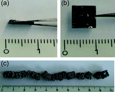 | ||
| Fig. 1 (a) and (b) HOPG before expansion. (c) HOPG after intercalation and expansion. | ||
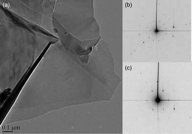 | ||
| Fig. 2 High purity graphene prepared by a chemical intercalation method (a) TEM overview of a graphene flake. (b) Electron diffraction of few-layer region, showing the stacking with orientational mismatch of the sheets. (c) Diffraction pattern from a single layer region. | ||
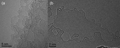 | ||
| Fig. 3 Atomic resolution, aberration-corrected TEM detail of graphene flakes (a) HRTEM micrograph of few-layer high purity graphene prepared by a chemical intercalation method. (b) HRTEM detail revealing the presence of clean, single, and bi-layer graphene areas. | ||
Raman spectroscopy
Raman spectroscopy is a fast and non-destructive method for the characterization of carbons and graphene can be readily identified in terms of the number of layers. Most sp2 carbon materials exhibit a strong Raman feature, the so-called G′ band, in the 2550–2850 cm−1 range. The shape and position of the G′ band can be used to differentiate the number of layers in FLG flakes.30Fig. 4 shows the G′ spectra of some representative flakes.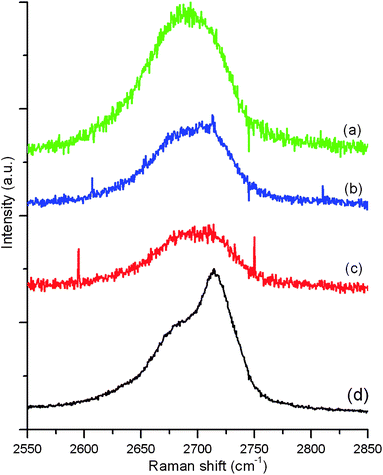 | ||
| Fig. 4 The G′ spectra of (a) monolayer graphene flake, (b) bi-layer graphene flake, (c) FLG fraphene flake and (d) HOPG. | ||
AFM of deposited flakes
Fig. 5 shows AFM of monolayer graphene and FLG flakes. Other workers used this technique to gauge the cleanness of the graphene produced.31 The presence of residual NMP between the graphene layers and the SiO2 substrate can lead to larger than expected flake thickness. This does not seem to be the case here.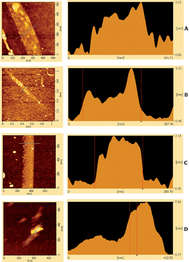
Fabrication of FETs
The graphene-ethanol mixtures used for thr TEM and HRTEM studies were allowed to stand so that the graphene settled out by gravity. The ethanol was pipetted off and replaced by NMP for the transport measurements. The graphene-NMP solution was used for the deposition in order to minimize non-directed deposition that would result from rapid drying of volatile solvents, such as ethanol. Micro-electrode arrays, consisting of 100 electrode pairs in a 100 μm × 100 μm region, were fabricated by electron-beam lithography followed by metallization with 10nm Ti and 50 nm Pd. Each array has one common electrode for all the devices, and one independent electrode for each device. This arrangement allows for simultaneous biasing of all devices by capacitive coupling, as has been previously used for large-scale assembly of carbon nanotubes, while allowing for independent electrical characterization of each device. The doped-Si back-gate, separated by 200 nm thick SiO2 dielectric, allows for three-terminal transport measurement in a field-effect transistor (FET) configuration. A region of this array, with 10 electrode pairs, is shown in Fig. 6a, each location bridged by a graphene flake deposited from suspension in NMP by dielectrophoresis. The detailed procedure for this has been described previously, along with systematic AFM, SEM and device characterization.32 The exfoliated graphene flakes were integrated into micro-electrode arrays by alternating-current (ac) dielectrophoresis (DEP), as we described recently.32 Due to the self-limiting nature of DEP deposition,33 only one flake is assembled at each device location. Fig. 6a shows ten typical devices. The devices exhibit ambipolar electric field effect with respect to the charge transport. Under gate bias (VG) conductance modulation of 50% was observed at room-temperature (Fig. 6c) consistent with previous reports on flakes obtained by micromechanical cleavage of bulk graphite3 and by thermal exfoliation of HOPG.34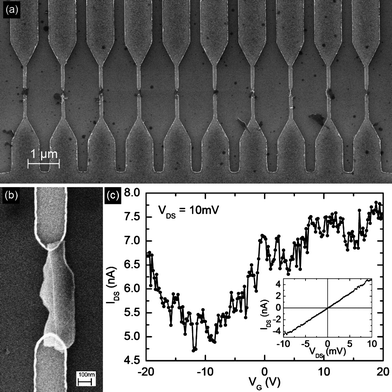 | ||
| Fig. 6 (a) Scanning electron micrograph of a region of the micro-electrode array showing 10 electrode pairs (b) SEM detail of one such device, and the corresponding FET transfer characteristics is shown in (c). | ||
The electronic properties of graphene differ from that of bulk graphite up to a thickness of about 10 layers35 and until this limit we refer to the material as ‘few layer graphene (FLG)’ as opposed to graphene (monolayer) or graphite (>10 layers). Therefore, devices fabricated with FLG flakes by DEP can be expected to show gate dependence of conductivity with a minimum non-zero conductance at the charge-equilibrium (Dirac) point.
Characterization
The experimental data were obtained using SEM (Leo 1530), Raman (JY T6400), AFM (Seiko Instruments Inc SPI-4000), TEM and TEM Diffraction (Tecnai F20 ST), HRTEM (TEAM 0.5 Microscope installed at NCEM). The atomic resolution, aberration corrected TEM measurements were performed as reported by Meyer et al.29 Agitation of the ethanol-graphene mixture was by hand and agitation of the NMP-graphene suspensions was carried out in a Bandelin Sonorex sonication bath. Electron transport measurements were conducted by mounting the chip in a ceramic package, wire-bonding, and measuring with a semiconductor parameter analyzer (Agilent 4155B) under N2 flow.Results and discussion
The ac-DEP route is independent of the graphene source and the graphene flakes can be subsequently patterned without prior AFM or SEM imaging as the location of the flakes and the orientation of the electrodes is predetermined. This overcomes many limitations in scalability and directed-assembly found in other fabrication routes.The majority charge carriers can be tuned between electrons and holes continuously, which is experimentally accomplished by sweeping the back-gate voltage between positive and negative values. Graphene's electron transport is described by the Dirac equation and this allows access to quantum electrodynamics in a simple condensed matter experiment.3,22,34,36 The point of charge neutrality, observed as a minimum in the transconductance characteristics at −10 V, is referred to as the Dirac point (Fig. 6c). It is significant to note that experimentally the carrier mobility in graphene only shows weak dependence on temperature indicating that it is limited by defect and impurity scattering at room temperature. The large noise in the devices is attributed to the fact that measurements were done in air, not in vacuum, and therefore carriers are subject to high degree of scattering from adsorbed gasses on the graphene flake. The devices shown in Fig. 4 consist of FLG flakes, which are sufficiently thin to exhibit gate-modulation of its conductance. Although monolayer graphene flakes were seen in AFM and Raman we were unable to locate any of them amongst the deposited devices, probably because the percentage of monolayers in the solution is small, and the dielectrophoretic deposition is additionally selective to thicker flakes since the dielectrophoretic force scales with volume of the flake. Efforts to produce predominantly monolayer flakes are currently under way to increase the yield of monolayer devices.
The observation of Dirac point in solution-phase exfoliated graphene serves to illustrate the quality of pristine graphene and the lack of significant residual covalent functionalization.
Conclusions
In summary, we have developed a simple method of fabricating few-layer and single-layer graphene which could be used for production on a gram scale. AFM, TEM, Raman and FET measurements all confirm that the process results in high yield of FLG flakes. An important point is that the graphene produced appears to be contamination free as shown from our atomic resolution HRTEM data. Gass et al.28 concluded in their recent paper “All detailed observations of graphene appear to show the presence of contamination, indicating that electrical measurements carried out on graphene are also on contaminated layers, even though this does not seem to significantly affect the electronic properties.” With our graphene this is not an issue. The diffraction patterns shown in Fig. 2a and 2b consist of distinct diffraction spots which reveal the crystalline nature of the graphene flakes. In particular, the diffraction patterns do not contain diffuse circular intensity halos which would indicate the presence of amorphous material. Therefore, we can conclude that the graphene flakes are clean and there is no evidence for any amorphous contamination layers. This is corroborated by the HRTEM micrographs shown in Fig. 3. Our FLG flakes were thin enough for the observation of the Dirac point, similar to FLG flakes recently made by thermal exfoliation34 and, unlike the mechanical exfoliation method favored by physicists, are also free of contamination from adhesive tapes or organic solvents. Although, at present, the flakes appear to fail at an order of magnitude lower than in other graphene devices there are a number of parameters to be optimized such as the graphene-on-electrode configuration rather than electrode-on-graphene. Work is also in progress to determine the exact nature of the intercalation species and to improve the yield of single layer graphene from the method.Acknowledgements
A.V. acknowledges funding by the Initiative and Networking Fund of the Helmholtz-Gemeinschaft Deutscher Forschungszentren (HGF). This work was partly supported by World Premier International Research Center Initiative (WPI Initiative) from MEXT, Japan and we thank Dr Taketoshi Fujita and Dr Yoshihiro Nemoto for technical assistance. Part of this work was performed at NCEM, which is supported by the Office of Science, Office of Basic Energy Sciences of the U.S. Department of Energy under Contract No. DE-AC02—05CH11231.Notes and references
- J. Wu, W. Pisula and K. Müllen, Chem. Rev., 2007, 107, 718 CrossRef CAS.
- B. C. Brodie, Philos. Trans. R. Soc. London, 1859, 149, 249 CrossRef.
- K. S. Novoselov, A. K. Geim, S. V. Morozov, D. Jiang, Y. Zhang, S. V. Dubonos and I. V. Grigorieva, Science, 2004, 306, 666 CrossRef CAS.
- W. S. Hummer and R. E. Offeman, J. Am. Chem. Soc., 1958, 80, 1339 CrossRef CAS.
- A. Lerf, H. He, M. Forster and J. Klinowski, J. Phys. Chem. B, 1998, 102, 4477 CrossRef CAS.
- K. A. Mkhoyan, A. W. Countryman, J. Silcox, D. A. Stewart, G. Eda, C. Mattevi, S. Miller and M. Chhowalla, Nano Lett., 2009, 9, 1058 CrossRef CAS.
- H. P. Boehm, A. Clauss, G. Fischer, U. Hofmann. Proceedings of the 5th Conference on Carbon, Pergamon Press. 1962, 73 Search PubMed.
- H. P. Boehm, A. Clauss, G. Fischer and U. Hofmann, Z. Naturforsch, 1962, 17b, 150 Search PubMed.
- D. Li, M. B. Müller, S. Gilje, R. B. Kaner and G. G. Wallace, Nat. Nanotechnol., 2008, 3, 101 CrossRef CAS.
- S. Stankovich, R. D. Piner, X. Chen, N. Wu, S. B. T. Nguyen and R. S. Ruoff, J. Mater. Chem., 2006, 16, 155 RSC.
- C. Gómez-Navarro, J. C. Meyer, R. S. Sundaram, A. Chuvilin, S. Kurasch, M. Burghard, K. Kern and U. Kaiser, Nano Lett., 2010, 10, 1144 CrossRef CAS.
- H. J. Shioyama, J. Mater. Sci. Lett., 2001, 20, 499 CrossRef.
- L. M. Viculis, J. J. Mack and R. B. Kaner, Science, 2003, 299, 1361 CrossRef CAS.
- A. K. Geim and K. S. Novoselov, Nat. Mater., 2007, 6, 183 CrossRef CAS.
- A. Böttcher, F. Hennrich, H. Rösner, S. Malik, M. M. Kappes, S. Lichtenberg, G. Schoch and O. Deutschmann, Carbon, 2007, 45, 1085 CrossRef.
- C. N. R. Rao, A. K. Sood, K. S. Subrahmanyam and A. Govindaraj, Angew. Chem., Int. Ed., 2009, 48, 7752 CrossRef CAS.
- K. P. Loh, Q. Bao, P. K. Ang and J. Yang, J. Mater. Chem., 2010, 20, 2277 RSC.
- L. B. Ebert, Annu. Rev. Mater. Sci., 1976, 6, 181 CrossRef CAS.
- A. Weiss, Angew. Chem., 1963, 75, 755 CrossRef CAS.
- H. P. Böhm and E. Stumpp, Carbon, 2007, 45, 1381 CrossRef CAS.
- M. Inagaki, R. Tashiro, Y. Washino and M. Toyoda, J. Phys. Chem. Solids, 2004, 65, 133 CrossRef CAS.
- X. Li, X. Wang, L. Zhang, S. Lee and H. Dai, Science, 2008, 319, 1229 CrossRef CAS.
- M. S. Dresselhaus and G. Dresselhaus, Adv. Phys., 2002, 51, 1 CrossRef CAS.
- S. F. McKay, J. Appl. Phys., 1964, 35, 1992 CAS.
- A. R. Ubbelohde and F. A. Lewis. Graphite and Its Crystal Compounds, Oxford University Press, New York, 1960, 151 Search PubMed.
- A. C. Ferrari, J. C. Meyer, V. Scardaci, C. Casiraghi, M. Lazzeri, F. Mauri, S. Piscanec, D. Jiang, K. S. Novoselov, S. Roth and A. K. Geim, Phys. Rev. Lett., 2006, 97, 187401 CrossRef CAS.
- C. Casiraghi, A. Hartschuh, E. Lidorikis, H. Qian, H. Harutyunyan, T. Gokus, K. S. Novoselov and A. C. Ferrari, Nano Lett., 2007, 7, 2711 CrossRef CAS.
- M. H. Gass, U. Bangert, A. L. Bleloch, P. Wang, R. R. Nair and A. K. Geim, Nat. Nanotechnol., 2008, 3, 676 CrossRef CAS.
- J. C. Meyer, C. Kisielowski, R. Erni, M. D. Rossell, M. F. Crommie and A. Zettl, Nano Lett., 2008, 8, 3582 CrossRef CAS.
- M. S. Dresselhaus, A. Jorio, M. Hofmann, G. Dresselhaus and R. Saito, Nano Lett., 2010, 10, 751 CrossRef CAS.
- Y. Hernandez, V. Nicolosi, M. Lotya, F. M. Blighe, Z. Sun, S. De, I. T. McGovern, B. Holland, M. Byrne, Y. K. Gun'Ko, J. J. Boland, P. Niraj, G. Duesberg, S. Krishnamurthy, R. Goodhue, J. Hutchison, V. Scardaci, A. C. Ferrari and J. N. Coleman, Nat. Nanotechnol., 2008, 3, 563 CrossRef CAS.
- A. Vijayaraghavan, C. Sciascia, S. Dehm, A. Lombardo, A. Bonetti, A. C. Ferrari and R. Krupke, ACS Nano, 2009, 3(7), 1729 CrossRef CAS.
- A. Vijayaraghavan, S. Blatt, D. Weissenberger, M. Oron-Carl, F. Hennrich, D. Gerthsen, H. Hahn and R. Krupke, Nano Lett., 2007, 7(6), 1556 CrossRef CAS.
- Y. B. Tang, C. S. Lee, Z. H. Chen, G. D. Yuan, Z. H. Kang, L. B. Luo, H. S. Song, Y. Liu, Z. B. He, W. J. Zhang, I. Bello and S. T. Lee, Nano Lett., 2009, 9, 1374 CrossRef CAS.
- B. Partoens and F. M. Peeters, Phys. Rev. B: Condens. Matter Mater. Phys., 2006, 74, 075404 CrossRef.
- K. S. Novoselov, A. K. Geim, S. V. Morozov, D. Jiang, M. I. Katsnelson, I. V. Grigorieva, S. V. Dubonos and A. A. Firsov, Nature, 2005, 438, 197 CrossRef.
| This journal is © The Royal Society of Chemistry 2010 |