Label-free biological and chemical sensors
Heather K.
Hunt
a and
Andrea M.
Armani
*b
aMork Family Department of Chemical Engineering and Materials Science, University of Southern California, 3651 Watt Way VHE 514, Los Angeles, CA, USA. E-mail: heather.hunt@usc.edu
bMork Family Department of Chemical Engineering and Materials Science and Ming Hsieh Department of Electrical Engineering, University of Southern California, 3651 Watt Way VHE 712, Los Angeles, CA, USA. E-mail: armani@usc.edu
First published on 30th June 2010
Abstract
Highly sensitive, label-free biodetection methods have applications in both the fundamental research and healthcare diagnostics arenas. Therefore, the development of new transduction methods and the improvement of the existing methods will significantly impact these areas. A brief overview of the different types of biosensors and the critical parameters governing their performance will be given. Additionally, a more in-depth discussion of optical devices, surface functionalization methods to increase device specificity, and fluidic techniques to improve sample delivery will be reviewed.
 Heather K. Hunt | Dr Heather Hunt received her BS in Chemical Engineering from Iowa State University (2004) and her PhD in Chemical Engineering from the California Institute of Technology (2009) in the research group of Prof. Mark E. Davis. She was awarded an NSF Graduate Research Fellowship for her doctoral work. Since 2009, she has been a post-doctoral scholar at the University of Southern California in the group of Prof. Andrea Armani. Her research interests include the design of novel nanostructured materials and devices for environmental monitoring and remediation. |
 Andrea M. Armani | Prof. Andrea Armani received her BA in physics from the University of Chicago (2001) and her PhD in applied physics with a minor in biology from the California Institute of Technology (2007), where she continued as the Clare Boothe Luce post-doctoral Fellow in biology and chemical engineering. She is currently the Fluor Early Career Chair of Engineering and an Assistant Professor of Chemical Engineering and Materials Science and Electrical Engineering–Electrophysics in the Viterbi School of Engineering at the University of Southern California. The research focus of the Armani lab is the design and optimization of novel optical devices for studying biological and chemical systems. Prof. Armani has received numerous awards, including the Sigma Xi award for excellence in research (2001), the SPIE BiOS Young Investigator Award (2008), ONR Young Investigator Award (2009), the Technology Review Top 35 Innovators under 35 (2009) and the USC Mellon Mentoring Award (2010). |
1 Background
Intra- and inter-cellular signal transduction describes the biochemical mechanism through which cells respond to environmental stimuli. Similar to electrical control circuits, these biological regulatory circuits or signaling pathways can be immensely complex, consisting of signaling cascades with multiple positive and negative control loops.1–7 Given that these pathways underpin all biological behavior, developing an understanding of signal transduction is therefore of significant importance, both in fundamental and applied research.8–13Unraveling these intricate co-dependent pathways requires multiple analytic methods used in parallel.14 For example, single cell fluorescent microscopy could be used to monitor the behavior and location of known proteins within the cell while western blots would determine the concentration of the signaling protein of interest that is produced in response to a given stimuli. While imaging is able to provide information about the physical behavior of the cell in real-time, the pivotal question is the production rate of the signaling protein.9–13 In contrast, if the signaling protein concentration is measured in real-time, the production rate will describe both the magnitude of the cellular response to the environment change and the time constant for the response.
To further complicate these experimental investigations, it has also been shown that a cell's behavior is dependent on its interactions with neighboring cells. In other words, ensemble measurements provide different results from single cell measurements. Therefore, while it is necessary to perform single cell studies to accurately map out a signaling pathway, ensemble measurements provide a more accurate picture of the magnitude of a given response. Additionally, both of these measurements need to be performed in real-time. However, while there are numerous techniques capable of measuring low concentrations at discrete time points, there are currently very few real-time detection methods.15–19
Therefore, it is necessary to develop improved, multi-modal, label-free sensing technologies that can provide the direct evidence needed.20 The new techniques need to be both sensitive and specific to the target molecule. Additionally, the detection method should be viable in multiple biological solutions. This necessity has spurred a recent surge in the development of innovative biosensing technologies, expanding the toolkit of biologists. These new techniques of detection are based on optical, electrical, magnetic, and mechanical principles.21 Optical devices are based on optical waveguides,22,23 surface plasmon waveguides and resonators,24 and split ring resonators. Electrical sensors typically involve monitoring the current across a gap; however, though based on this simple principle, they are fabricated from a wide range of materials, including nanotubes and wires,25 nanocrystals, polymers, and conventional semiconductors.26 Mechanical sensors or cantilevers are typically lithographically fabricated and can be used in a deflection or vibration mode.27,28
However, like any detection modality, label-free detection methods must be both sensitive and specific. In the case of label-free methods, this task is typically divided between the device and the surface functionalization method. Specificity or selectivity of a sensor for a given molecule is provided through chemical modification of the device's surface.29–31 The selectivity of the sensor for a given molecule is dependent on the quality of the surface functionalization method used (i.e. antibody, antigen, µRNA, synthetic antibody, etc.).
There are other equally important parameters which determine a sensor's practicality, such as collection efficiency and signal![[thin space (1/6-em)]](https://www.rsc.org/images/entities/char_2009.gif) :noise. The collection efficiency of the sensor, or the ability of the sensor to detect a biological element in its vicinity, is crucial. By passivating the non-active surfaces and creating directed flows to the active sensor surfaces, the collection efficiency can be increased.32–35 The signal:noise (SNR) is dependent on the type of sensing modality and the environment around the sensor.
:noise. The collection efficiency of the sensor, or the ability of the sensor to detect a biological element in its vicinity, is crucial. By passivating the non-active surfaces and creating directed flows to the active sensor surfaces, the collection efficiency can be increased.32–35 The signal:noise (SNR) is dependent on the type of sensing modality and the environment around the sensor.
This review will give a brief overview of the label-free sensing methods and the metrics that are used to characterize sensing performance in the bio-domain, focusing primarily on the optical methods. It will also give a survey of the methods that can be used to endow a sensor with specificity, a characteristic that is equally, if not more, important in some applications than sensitivity. Finally, it will review some of the methods which can be employed to improve sample delivery to the sensor surface and decrease the amount of sample which is necessary to perform a measurement.
1.1 Sensor terminology
There are two general classes of transducers: input transducers or sensors and output transducers or actuators. This review article focuses on the former. Briefly, in an input transducer, the signal of interest is detected by the transducer, which generates a recordable signal. The most common type of input transducer is a thermometer. In contrast, in an output transducer, such as nerve endings in your finger, a source signal triggers the transducer to generate a physical signal. All of the transducers in the present review are considered input transducers or sensors. Therefore, we use transducer and sensor interchangeably in the proceeding discussion.In a static configuration, the relationship between the sensor output signal and the measurand is S = a + bs, where S is the electrical signal produced with “s” measurand, a is the intercept or the output signal at zero input signal, and b is the slope or sensitivity of the transducer. However, this relationship assumes that the response of the sensor is perfectly linear, which is usually not the case. To further explore this, it is necessary to define the dynamic range and the dynamic characteristics of the sensor—in other words, the non-static behavior of the sensor. A more in-depth discussion of this topic can be found in a variety of textbooks, and it is merely being reviewed here to standardize terminology for the rest of this article.36,37
One of the most commonly reported metrics of a sensor is the threshold sensitivity or limit of detection (LOD). This term refers to the minimum concentration of a measurand which is detectable. Although researchers use this term interchangeably, the technical term is limit of detection.38 This value is dependent not only on the sensor, but also on the noise of the system.
The dynamic range describes the range of measurand values that are detectable by the sensor, or the minimum and maximum measurand values that generate a response in the sensor (Fig. 1). Specifically, it is described by the full scale output (FSO), linearity and hysteresis of the sensor. The FSO is the maximum output signal over the dynamic range or the difference in output between the highest and lowest values. Linearity describes closeness of the sensor's calibration curve to a straight line. This is typically expressed as a percent of the FSO. Hysteresis is the maximum difference in output at any measured value when the value is approached first with an increasing and then with a decreasing input.
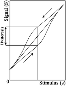 | ||
| Fig. 1 Conventional sensogram showing the relationship between stimulus (s) and signal (S). As indicated by the arrows, hysteresis describes the difference in the forward and reverse response of the sensor. | ||
Related parameters include saturation, selectivity, sensitivity shift, zero-measurand output, and zero shift or drift. Saturation is the point at which there is no further output signal, even if more measurand is added to the sensor. Selectivity describes the suppression of incorrect signals, such as binding of incorrect biological molecules or environmental interference.
While the above parameters describe the fundamental characteristics of a sensor, there are numerous others worth briefly mentioning. The warm-up time and frequency response describe how fast a sensor can respond to a measurand. It is important to make sure that a sensor has a faster response time than the measurand under study. Finally, the repeatability/reproducibility of the sensor describes how the response of the sensor changes if the same measurement is performed under the same conditions. This is dependent on metrics such as the false positive and the false negative rate.38
1.2 Transduction mechanisms
As mentioned, label-free detection typically is performed using an optical, mechanical or electrical transducer (Table 1).20,39,40 As a result of their transduction mechanisms, all of these methods are sensitive; however, in order to detect a specific analyte, they all require surface modification. While the focus of this review article is optical transducers, for comparison, we provide a brief summary of electrical and mechanical methods here.| Modality | Electrical | Mechanical | Optical |
|---|---|---|---|
| Detection signal (change in) | Current, resistance, voltage | Mechanical resonant frequency, strain/stress deflection | Intensity, optical resonant frequency, interference signal |
| Devices | Nanowire, nanopore | Cantilever (passive), resonator (active) | Microcavity, waveguide |
| Example detections | Nanowire: single virus44,45 | Cantilever: single cell27 | Microcavity: single virus and molecule58,59 |
| Nanopore: single DNA41,42 | Resonator: pM DNA184 | Waveguide: ∼100 cells63,185 |
Because these devices are typically fabricated using lithographic techniques, it is possible to develop a completely integrated system, with the sensor and detector on a single platform. Additionally, with the recent innovations in power harvesting, it may soon be possible to have an autonomous electrical sensor for continuous environmental monitoring.
One recent and very significant example of this technique combined antibody mimic proteins with In2O3 nanowire based field effect transistor (FET) biosensors to detect nucleocapsid (N) protein, which is a biomarker for severe acute respiratory syndrome (SARS).46 The surface of the In2O3 nanowire sensor device shown in the inset of Fig. 2 was first functionalized using antibody mimic proteins (AMPs) to improve the ability of the device to detect N protein. Unlike polyclonal or monoclonal antibodies, AMPs are engineered to target a specific analyte, and they can be designed to be stable in a wide range of environments. Therefore, this new class of targeting moiety is ideal for biosensor surface specification.47–50Fig. 2 shows the response of the FET biosensor, functionalized with the AMP, when it is exposed to the indicated nM concentrations of N protein. This experiment was the first demonstration of both AMPs as recognition elements for sensor applications, and this level of detection in complex media (bovine serum albumin).
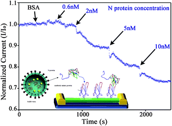 | ||
| Fig. 2 Detection using an In2O3 nanowire FET sensor functionalized with an antibody mimic protein (AMP). The black arrows indicate the times when the solution was raised to the indicated concentration of N protein. Inset: schematic diagram showing the AMP immobilized on the surface of the nanowire FET device. The AMP was attached to the NWs via the sulfydryl group of a cysteine near the C-terminus, remote from the binding site. The AMP probe was used to capture the N protein. N protein is biomarker for SARS. Adapted with permission from ref. 46. © 2009 American Chemical Society. | ||
| Δh = 3σ(1 − ν)/E × (L/d)2 |
One of the initial demonstrations of the utility of the microcantilever sensor was given by Wu et al. (shown in Fig. 3a).54 In this experiment, the cantilever (Fig. 3a, inset) detected ultra-low concentrations of prostate specific antigen (PSA), a biomarker for prostate cancer, in complex media, such as BSA (bovine serum albumin) and HSA (human serum albumin). As the concentration of the PSA in the media increased, the deflection of the cantilever increased. Several cantilever sensor parameters were characterized during these experiments, including the dependence of the signal on the length and thickness of the cantilever, and the sensitivity of the signal to thermal drifts within the system. As can be seen in Fig. 3b, by optimizing this device, it was possible to detect PSA at clinically relevant concentrations.54
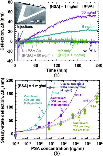 | ||
| Fig. 3 Detection of free prostate specific antigen (PSA) using micro-mechanical cantilevers. (a) Specificity of fPSA detection against a high background of human serum proteins, namely, human serum albumin (HSA) and human plasminogen (HP), both at concentrations of 1 mg ml−1. The cantilevers used were 200 µm long and 0.5 µm thick and made of silicon nitride. Inset: SEM image of a microcantilever. (b) Steady-state cantilever deflections as a function of fPSA and cPSA concentrations for three different cantilever geometries. Note that longer cantilevers produce larger deflections for the same PSA concentration, thereby providing higher sensitivity. Using 600 µm long and 0.65 µm thick silicon nitride cantilevers, it was feasible to detect fPSA concentration of 0.2 ng ml−1. Every data point on this plot represents an average of cantilever deflections obtained in multiple experiments done with different cantilevers, whereas the range of deflections obtained from these experiments is shown as the error bar. The only exception is the data for fPSA detection using 200 µm cantilevers, where the data (green diamonds) from multiple experiments at a given concentration are shown as a cluster plot. The error bar in each of these data points represents the fluctuation of the cantilever during the particular measurement. Adapted by permission from Macmillan Publishers Ltd: Nature Biotechnology, ref. 54 © 2001. | ||
However, the cantilever is also a mechanical resonator, with discrete resonant frequencies that are dependent on all of the properties of the device. In this “active” configuration, the governing equation is:
 | (1) |
Recently, researchers have leveraged this detection method to increase the sensitivity of the device. In this configuration, the resonant frequency is monitored, and it is possible to measure single cell binding events.27
2 Optical detection
Optical detection is performed by exploiting the interaction of the optical field with its environment. While this sounds relatively simple, there are numerous methods of implementation. In this section, three of these will be discussed: (1) general evanescent-field based methods, (2) resonant cavity-based methods, and (3) surface plasmon-based methods. An overview of these different methods is contained in Table 1.2.1 Evanescent field devices
The field of evanescent sensing was first proposed in the 1960's based on spectroscopy and total internal reflection measurements.55,56 In an evanescent field sensor, the optical field is divided between the waveguiding material and the volume around the sensor. Therefore, the optical field directly interacts with any molecules or cells that bind to the sensor surface. Since its conception, evanescent field detection has been realized in many device geometries and platforms and has been integrated with microfluidics, creating the burgeoning field of optofluidics.20,57 While other types of optical sensors, such as resonant microcavities, have higher sensitivity, waveguides are not bandwidth-limited, making them ideal for handheld applications.58,59Optical waveguides are designed to confine and to direct electromagnetic fields along a specific path. The important features of waveguides are their levels of dispersion and optical loss. If the refractive index is dependent on the wavelength, then the dispersion is significant and leads to bandwidth limitations on the waveguide. The optical loss is comprised of both the material or absorption loss and the scattering defects.60,61
Because high performance, integrated waveguides will be a crucial element in the development of optical computing, a significant amount of research has been invested in developing this seemingly simple structure.62 It is important to note that while optical fiber clearly has better performance than either photonic crystal or slab devices, it also is not integrated into a chip. Therefore, the latter types of waveguides are preferred for portable applications, such as biosensors.
The relative simplicity of the optical sensing mechanism endows it with a great degree of flexibility in its implementation. There are two primary sensing methods: (1) directly inducing an optical change in the sensor (refractive index, dielectric constant) or (2) spectroscopically probing the molecule of interest. While the latter method has improved resolution over the former, it is also more complex in its implementation, requiring either a narrow linewidth tunable laser source or an array of narrow linewidth lasers for the spectroscopic measurement. There have been preliminary demonstrations of integrated laser arrays based on Vertical-Cavity Surface-Emitting Lasers (VCSEL).21
To increase the sensitivity, but still use a fixed wavelength source, it is possible to use a technique known as interferometry.63 In this method, one of three changes in the propagating light beam is measured: path length, wavelength or propagation speed. In waveguide sensors, the refractive index (propagation speed) is the dominant detection mechanism. Two key parameters are used to characterize the performance of an evanescent waveguide sensor: penetration depth and threshold sensitivity.
The penetration depth characterizes the overlap of the evanescent field with the environment. In this respect, it is desirable to have as large a penetration depth as possible, to increase the detection area. On the other hand, the loss of the evanescent field within the environment is typically larger than that of the waveguide, which can reduce the overall device sensitivity. For example, the expression for penetration depth (dp) is:
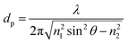 | (2) |
As can be seen, the penetration depth is dependent on wavelength. Therefore, an initial approach would be to operate at longer wavelengths, near-IR to IR, to maximize the penetration depth. However, the absorption of water at these wavelengths is extremely high. In fact, at 600 nm, the loss of water is 0.002 cm−1 whereas at 1540 nm the loss is 11.8 cm−1.64 This increase in loss of the device nullifies any benefit that the increase in penetration depth might provide. Therefore, there is a balance between increasing the penetration depth, which increases the detection efficiency, and increasing the loss of the device, which negatively effects both the signal:noise and the sensitivity.
Initial experiments performed using waveguide sensors compared input power (Pi) to output power (Pf) as a simple ratio, and related the change to the bound analyte. However, this method of detection is extremely sensitive to environmental changes (primarily temperature). Therefore, a more complex method of detection was implemented based on an integrated Mach–Zehnder Interferometer (MZI).
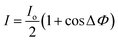
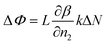
In interferometric detection, environmental effects are normalized out of the signal by the application of the reference arm which is located in the proximity of the sample arm. Detection is performed by monitoring the phase change in the signal. By monitoring the phase of the signal, instead of the power, the effect of laser instabilities on the detection measurement is also minimized. The precise governing equations are shown below:
 | (3) |
 | (4) |
 | (5) |
 | (6) |
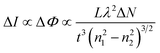
One observation that can be made from these equations is that a longer waveguide sensor produces a larger signal (ΔΦ) at a given wavelength. However, the high loss of the currently available integrated waveguide devices restricts the sensitivity. As the loss decreases, the SNR increases. Therefore, by improving the fundamental optical device, the sensitivity of the biosensor will also improve. This is currently an active area of research by many groups in this field.
2.2 Resonant cavities
An extension or subset of evanescent-based detection, optical resonant cavities confine light of a discrete set of wavelengths which are defined by the cavity.65–68 As molecules bind to the surface of the cavity, these wavelengths change. Therefore, while it is possible to perform detection by monitoring the power, much higher sensitivity is achieved by monitoring changes in the resonant frequency of the device.The primary figure of merit for a resonant cavity is the Quality factor or Q of the cavity. The common figure of merit for optical cavities is the quality factor or Q of the cavity. This term describes the photon lifetime (τo) within the cavity, which is directly related to the optical losses of the cavity. Therefore, a device with a high Q factor has low optical losses, long photon lifetimes or a long photon decay rates (1/τo).61,68 As a result of their compact geometry and large build-up power, optical cavities have numerous applications throughout science and engineering, including fundamental physics studies, biophysics, and telecommunications.20,58,59,61,67,69–80
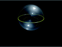
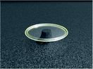
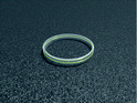
Depending on how the optical field is confined inside the cavity, it is either a standing wave (Fig. 4a) or a traveling wave cavity (Fig. 4b and c).58,81 In either type, the optical field is not completely confined, enabling it to interact and sense changes in the environment.
 | ||
| Fig. 4 Finite element method simulations showing the distribution of the optical field in (a) standing wave and (b and c) traveling wave resonant cavities. Insets: scanning electron micrographs of the specific cavity geometries being modeled: (a) photonic crystal cavity, (b) microdisk resonator and (c) microtoroid resonator. Part (a) is adapted from ref. 81. © 2009 RSC. | ||
By using a tunable narrow-linewidth laser and scanning over a series of wavelengths, specific resonant frequencies can be selectively excited and detected. For coupling light into planar devices, both tapered optical fiber couplers and prism couplers have been used; however, tapered optical fibers have lower losses, and are therefore higher efficiency couplers of light.82,83
One advantage of label-free methods is the ability to perform detection in real-time, which allows for data to be taken continuously while other biologically relevant parameters (such as temperature, pH, salt) are changed. Several geometries of microcavities have already been integrated with semi-automated or automated microfluidic delivery systems to further enable complex biological investigations.
Previous traveling wave or whispering gallery mode microcavity detection experiments have been performed using a wide range of geometries and materials.84–88 An overview of these experiments and the microcavities used is contained in Table 2. In all of these microcavities, detection occurs when a molecule interacts with the evanescent optical field of the microcavity. However, because the location and mode profile of the field are very different, the magnitude of the signal varies between the cavities. Additionally, the molecule delivery method is different. In the case of the microsphere, microtoroid and microring, the analytes are delivered over the sensor surface and bind to it. In contrast, in the liquid core optical ring resonator (LCORR), the solution is flowed through (inside) the device.
|
|
|
|
|
|
|---|---|---|---|---|
| Geometry | Microsphere65,91,92,95 | Microtoroid58,94,186 | Microring77,84,187 | LCORR20,76 |
| Possible material | Silica | Silica | Polymeric materials, silicon | Silica |
| Quality factor (in air) | >109 | >108 | ∼103 to 105 | ∼103 to 105 |
| Quality factor (in water) | >106 | >108 | ∼103 to 105 | ∼103 to 105 |
| Detection demonstrations | Single virus, cis/trans of protein, DNA | Single molecule in buffer and in serum, fluorophore | Detection of bacteria, glucose | Detection of DNA, proteins |
The detection mechanism for optical cavities is similar to that of optical waveguides. The optical field interacts and polarizes each molecule that binds to the surface of the cavity, thus changing the cavity's refractive index. This change is detected as a shift in the resonant frequency of the device. The interaction between the optical field and a bound molecule can be described by an application of Maxwell's equations to the simple governing relations of optical microcavities. An optical cavity's resonance condition is defined by the wavelength λ for which the cavity's circumference is an integer multiple of the orbital wavelengths. Therefore, the resonant wavelength must change for any change in the cavity radius (R) or refractive index (n) according to the following:59,87–90
 | (7) |
If you extend this to the case in which, for instance, a protein is non-uniformly distributed across the cavity surface, a more complex analysis becomes necessary. In this situation, each particle is polarized by the optical field, according to the excess polarizability of the particle (αex). Taking into account the global effect of all the bound molecules by incorporating their surface density (σ), the expression for the resonant frequency shift in this domain, in the case of a sphere, becomes:59,87–92
 | (8) |
It is important to note that, although the magnitude of the shift increases as the radius of the cavity decreases, the radius of the cavity also determines the quality factor of the cavity. Therefore, a more useful expression for detection applications is the threshold sensitivity or limit of detection. This metric is determined by setting the resonant frequency shift to the resonance linewidth (δλ = Δλ = λ/Q). This expression captures the lowest surface density of bound molecules that a given cavity can detect, and is dependent on the cavity Q factor, both for the re-circulation of light and for the narrow resolution.
This basic detection mechanism has been verified using many different geometries of optical resonant cavities and over a wide range of analyte concentrations.20,58,59,74,85–88,93 However, when this analysis is extended to the limit of single molecule detection, it must be modified, primarily in the dependence on the radius of the microcavity (R) and in the nature of the optical field interaction. Therefore, not surprisingly, there is a disconnect between the high concentration and the single molecule theory.
As has been shown by several research groups, the magnitude of single molecule resonant frequency shift depends on where a molecule binds to the surface of the resonant cavity. If a molecule binds at a region of higher field intensity (at the equator), the shift will be larger than if it binds at a region of lower field intensity. Therefore, the single molecule resonant frequency shifts are typically plotted as a distribution of shifts, which directly relates to molecule binding throughout this field.58,94,95
Standing wave resonant cavities or photonic crystal cavities perform detection based on a similar mechanism. However, because the optical field is more tightly confined, these devices have increased sensitivity over the more classic whispering gallery mode sensors.96–98
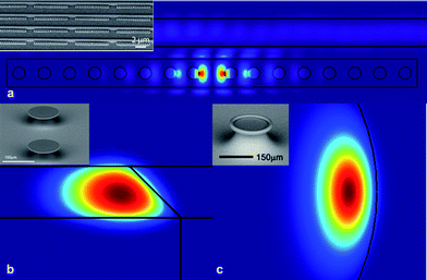
An example of a photonic crystal resonator sensor is shown in Fig. 5A.81 As can be seen in the inset, these devices can be fabricated in large arrays on SOI wafers.99 To perform detection of antibodies, the surface of the resonator was first functionalized with antigens. To improve the detection accuracy of the sensor, it was multiplexed with a control resonator, which removed any environmental effects (thermal drifts, laser fluctuations, etc.) from the detection signal.
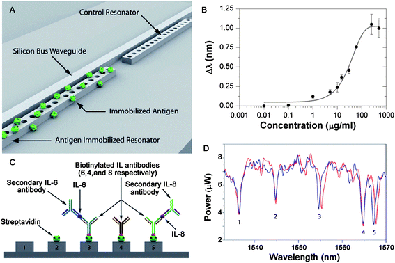 | ||
| Fig. 5 Optofluidic detection. (A) Artistic rendering showing a pair of photonic crystal resonant cavities which are coupled to a silicon waveguide. The first cavity is surface functionalized to target a specific moiety whereas the second cavity acts as a reference. (B) Streptavidin/anti-streptavidin response curve showing the working range of a device designed to target anti-streptavidin. (C) Schematic of a multiplexed resonant cavity array designed to distinguish between IL-4, IL-6, and IL-8 using five resonant cavities. (D) Detection and discrimination of a series of IL's using a multiplexed resonant cavity array such as that shown in part (C). The blue trace is the initial baseline location of each resonator. The red line shows the position of the resonance after both IL-6 and IL-8 and their associated secondary antibodies have been injected. Adapted from ref. 81. © 2009 RSC. | ||
A series of experiments were performed with this device to demonstrate both the working range and the detection sensitivity and specificity. For instance, Fig. 5B shows the dose–response curve for anti-streptavidin. This curve was acquired by incrementally exposing the surface of a streptavidin-functionalized device to increasing concentrations of anti-streptavidin. The data in Fig. 5B are fitted to a sigmoidal dose–response model, indicating that this is a high sensitivity device.81
To demonstrate that this device could perform both specific and sensitive detection, the researchers functionalized the surface of individual resonators using a series of interleukin antibodies (IL-4, IL-6, and IL-8), as shown in Fig. 5C. Subsequently, they exposed the multiplexed sensor to a series of solutions containing IL-8, IL-6, then secondary antibodies for each of these. As can be easily seen in Fig. 5D, only if the correct IL was present, did the resonant frequency change.81 The ability to perform low concentration detection in complex environments, with similar but incorrect antigens present, is extremely important for many applications, especially diagnostics.
2.3 Surface plasmon devices
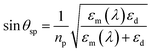
A surface plasmon or surface plasmon-polariton (SPP) is an electromagnetic wave which propagates at a metal–dieletric interface. The conditions for generating a surface plasmon mode are dependent on the geometry of the plasmonic structure and the environmental parameters. Therefore, any changes in the environment, such as the binding of biomolecules to the surface of the metal film, will change the plasmon mode.There are many different methods of performing detection using surface plasmon resonance.100–104 These are typically defined by the method of detecting the sensing signal, such as spectral, angular and localized.39 In angular detection, transverse polarized light is incident on a coupling prism, generating an evanescent field. Because this field is non-propagating at the majority of frequencies/conditions, the optical power is reflected back into a photodetector, with minimal loss. However, at specific angles of incidence (θsp), the energy is coupled into the metal film generating the surface plasmon mode. This is detected as a reduction in power and is described by:101
 | (9) |
It is important to note that εm is dependent on wavelength. Spectral surface plasmon detection exploits this dependence to monitor the coupling conditions between the incident wave and the generated plasmon. The primary difference between angular and spectral detection is in the realization or experimental apparatus. In angular detection, the incident angle is varied, and the wavelength is constant. In spectral detection, the incident angle is constant and the wavelength scanned.
An emerging field in surface plasmon detection is based on highly localized plasmon fields. These can be generated using ordered arrays of nanoparticles or nanohole arrays, instead of thin metal films. By creating more localized optical fields, the sensitivity of the device to changes in the environmental dielectric is greatly increased.
One example is shown in Fig. 6a. Using an array of ordered nanoholes and monitoring the change in the surface plasmon resonance peak, the researchers were able to demonstrate sensing limits of 5E-6 and 1E-5 refractive index units for orthogonal (OP) and parallel (PP) polarized light. The difference between the OP and PP detection sensitivities relates to the linewidth of the resonance or the resolution of the measurement.105
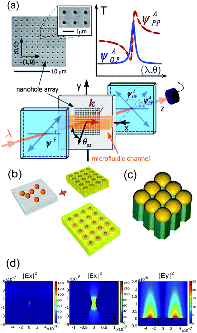 | ||
| Fig. 6 Surface Plasmon Resonance (SPR) based detection (a). Conceptual diagram of the 2-D nanohole-array-based SPR sensor. The input and output polarization states of a tunable laser are controlled, providing variable spectral or angular Fano-type profiles. A microfludic channel is used to transport the analyte fluid to the surface of the sensing area and can be used to control the refractive index on the metal–dielectric interface to tune the SPP resonance frequency. Also shown is a scanning electron microscopy image of a fabricated nanohole array sample. (b) Conceptual diagram of a 3-D nanoresonator array structure combining LSPRs and SPP in a metal film perforated by 2-D nanohole. (c) Schematic diagram of the proposed nanovoid geometry for practical realization of LSPRs coupled with SPP in a 2-D metal film perforated with nanohole. (d) Near-field FEM simulation of the intensity distribution of the electric field in the nanoresonant substrate on the water–metal interface. Surface sensitivity enhancement is verified. Adapted from ref. 105 and 106. © 2006, © 2009 Optical Society of America. | ||
One possible method of improving the detection is to combine techniques. For example, by combining the nanohole array with nanoparticles, it will be possible to create a device with both localized surface plasmons and surface plasmon-polaritons (Fig. 6b and c). As shown in the simulations of this hybrid structure (Fig. 6d), there are significant resonant behaviors for both Ex and Ey. Therefore, the resonant behavior of this device will increase the sensitivity to subtle changes in the environment.106
3 Biochemical surface functionalization methods
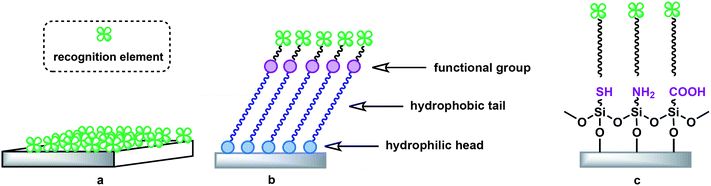
In order to interface with specific biological or chemical compounds, the various optical transducers mentioned above must include recognition moieties particular to the measurand. In this case, the recognition moiety is responsible for the transducer's ability to selectively detect the measurand of interest, while the transducer itself then converts the recognition event (often binding of the measurand to the surface of the transducer) into a measurable optical or electrical signal, as previously discussed. Integration of biological or chemical elements with these solid-state devices therefore enables both the (reversible and specific) interaction of the device with the measurand, and the final signal transduction. The exact protocols for the addition of specificity to a given device depend to a large extent on the proper selection and combination of the optical transducer type, the material(s) used to construct the said device, and the measurand itself. In this section, we discuss several general techniques for lending specificity to highly sensitive, label-free optical transducers. Although many of the techniques described below can also be utilized to create highly specific chemical sensors, for convenience, we refer primarily to the creation of biosensor devices.3.1 Recognition elements
The first step in the creation of a biosensor from an optical transducer is the appropriate selection of a recognition moiety for a targeted measurand. The selection should take into consideration the following capabilities of the recognition element in order to promote excellent sensor performance:(1) the element should be highly specific toward the measurand,
(2) the element should have a high affinity for the measurand,
(3) the element should form a reasonably stable complex with the measurand,
(4) the complexation or other interaction event between the element and measurand should be detectable by the optical transducer, and.
(5) the specificity and affinity of the element should not be altered significantly by its immobilization on the surface of the optical transducer.107–109
Due to continuing improvements in the fields of biochemistry and molecular biology, a diverse array of biological recognition moieties exists (or can be engineered) with the particular specificities and affinities required for a wide range of measurands.110,111 For instance, optical transducers have been paired with enzymes,112,113 peptides,114–116 antibodies (or antibody fragments),108,113,117–119 aptamers,43,120 and receptors121–125 as recognition elements. The biosensors created by the selection of these recognition elements can be categorized according to the type of event they monitor, and are commonly referred to as either biocatalytic or bioaffinity biosensors. The former uses the presence of enzymes on the surface of the transducer to catalyze a biochemical reaction, thus tracking the reaction, while the second monitors the binding of various biomolecular recognition elements, such as proteins, peptides, receptors, antibodies, etc., to the surface using binding moieties that are specific to the measurand.108 Therefore, the selection of the recognition element, and consequently the classification of the biosensor, will depend on the measurand targeted. Biosensors that utilize antibodies or antibody fragments as their recognition element form a subset of the bioaffinity family of biosensors known as “immunosensors.”
An interesting alternative to the use of actual biochemical molecules as recognition elements is the use of molecular imprinting to form “pockets” that are highly specific (that is, with a specificity similar to that of antibody–antigen interactions) in terms of a particular molecule, functional group, or structure type, towards the measurand.108 This technique is performed by coating the surface of the transducer with a solution containing both plastic monomers and the measurand. These components can then interact in the solution to create a low-energy network comprised of the two constituents. The coating is then polymerized, which results in the measurand becoming enfolded or entrapped within the polymer structure. After polymerization, the measurand can be removed by elution, leaving behind a rigid polymer structure with a template “pocket” that can be used to bind the measurand due to its shape and size selectivity. Molecular imprinting is therefore an attractive alternative when a recognition element cannot be found with the correct properties to produce excellent sensor performance.126–129 We refer the interested reader to the excellent reviews of this technique by Alexander et al., and Ye and Mosbach.130,131
3.2 Immobilization techniques
A number of parameters exist in the creation of biosensors that affect the final success of the device. The goal of most immobilization techniques is to create a recognition surface on the optical transducer that is capable of interacting with the measurand with high specificity, speed, and reliability, while maintaining the original sensitivity of the optical transducer. This suggests that the immobilization techniques should be tailored to the optical transducer and measurand, such that the surface functionalities generated through the chosen technique have low optical absorption, high density packing, high binding efficiency, specificity to only the target ligand, and reasonable stability in air and the testing media. Additionally, the technique should create a robust sensor surface that is not easily damaged or degraded, and ideally can be used multiple times without severely affecting the binding ability of the recognition moiety. Some of the key parameters that influence the biosensor properties listed above, and that should be investigated for a given measurand, include the effect of immobilization on the recognition element, the orientation (and its effect on the affinity) of the recognition element, and the effect of variations in surface coverage of the recognition element on its recognition capabilities.Lastly, consideration should be given to the ability of the sensor surface to be regenerated.107,109 The ability of biosensors to be used in a semi-continuous process, such that the biosensor does not need to be replaced between every use, is highly desirable, especially for medical diagnostics or “lab-on-a-chip” applications as this can reduce costs (for instance, of fabrication) and improve the repeatability of the detection measurements. However, Hock showed in his review of immunosensors that although antibody/antigen interactions are reversible, the recognition event is kinetically driven, and therefore high device sensitivity and fast regeneration ability are mutually exclusive capabilities for immunosensors.132 The selection of an appropriate regeneration technique depends upon the type of interaction(s) between the recognition element and the measurand (covalent coupling, hydrogen bonding, van der Waals forces, electrostatic forces, etc.), as well as the strength of that interaction. Dissociation of the bound complex can occur by changes in environmental conditions; for instance, antibodies are known to be sensitive to changes in pH, which can then be used to “encourage” the antibody to release its antigen.108,113 However, care must be taken in such cases, as the reagents used to create environmental changes can negatively impact the binding ability of the recognition element and therefore reduce the overall lifetime of the device.108 Alternatively, dissociation can be prompted by displacement of the complexed measurand with a biochemically similar analyte for which the recognition element has a weaker affinity.108 If this element is present at high enough concentrations, it should be able to successfully displace the measurand, which can then easily displace the analyte during detection. Lastly, in some cases, interchanging the recognition element and the measurand can lead to improved regeneration ability; for instance, replacing antibodies, whose tertiary structure is sensitive to pH, with the corresponding antigen, leads to more reusable immunosensors.113
There are a number of routes to functionalize surfaces using covalent coupling. For metal oxide surfaces, such as TiO2 or SiO2 (both commonly used to create optical transducers) the first step is generally to create surface hydroxyl groups which can then be attached to amines, thiols, carboxylates, etc.via linker agents during the second step. For silica-based materials, these conversion routes frequently involve the use of silane coupling agents, which can either be hydrolyzed to form a silica-based polymeric coating on a substrate via surface condensation, or reacted with surface silanols, without self-hydrolysis, to form a covalently attached monolayer on the substrate via grafting. Generally, the latter technique is preferred because the resulting monolayer promotes a high binding efficiency of target molecules, and is less likely than a thick silane layer to negatively affect the performance of the optical transducer due to absorption issues. Silane coupling to silica surfaces via the grafting technique is a well-understood process, and is easily carried out using organic solvent deposition or vapor deposition techniques. The resulting chemical functionalities on the surface can be further modified for attachment to the recognition element of interest via typical bioconjugate procedures.
Two typical examples of such bioconjugation protocols include N-hydroxysuccinimide (NHS) ester chemistry and “click” chemistry. NHS esters readily react with primary amines on a recognition element to form a stable amide bond. NHS ester groups can be generated on an optical transducer surface by silanizing the surface in a variety of ways; a typical method is the reaction of N,N′-disuccinimidyl carbonate (DSC) with amine-terminated silane surface groups. As an alternative example, heterobifunctional linkers terminated with NHS ester groups on one tail can be attached to the surface via reaction of the functional group on the other tail with the appropriate functional group on the surface (for instance, a maleimide–polyethylene glycol–NHS ester heterobifunctional linker can be attached to a thiol-modified surface through standard Michael Addition conditions). In such cases, the length of the linker can be adjusted based on the sensor requirements.
“Click” chemistry is an increasingly popular approach to the covalent coupling of recognition elements.142 For example, heterobifunctional linkers based on a polyethylene glycol (PEG) molecule, with a silane functionality at one end and an alkyne group at the other end, can be covalently bonded to the surface of the optical transducer. A second linker molecule, with an azide on one end, is then attached to the recognition element in such a way as to not interfere with its ability to recognize the measurand. Click chemistry is then used to “click” the azide-modified recognition element to the alkyne-modified substrate via a cycloaddition reaction which is usually quantitative.58 The primary advantage of this approach is that the alkyne will only bind with the azide functionality, and will not bind with other functionalities found in biological entities, resulting in a surface that is, in a sense, passive, if not all the alkyne groups on the surface are bound to the probe molecules. Additionally, the end product is stable under ambient conditions, and the terminal probe molecule can be interchanged easily, allowing for a wide array of probes to be examined. The disadvantage of this method is that the recognition element must be modified prior to attachment to contain an azide functionality.
The approaches discussed here represent only a general overview of the available routes for the bioconjugation of transducer surfaces, and many of the routes have similar or overlapping features. Several excellent reviews have delved further into the methods by which surfaces can be modified, as well as their applications. For instance, Kalia and Raines' review on bioconjugation techniques gives detailed information regarding different types of covalent coupling linkages, as well as recent advances in those protocols that allow for site-specific bioconjugation that reduces impacts on the active centers of biomolecules.143 Additionally, Knopp et al.'s recent review on the applications of bioconjugated, silica nanoparticles provides further detail on protocols for physical adsorption on and covalent coupling to silica surfaces.144 Lastly, an earlier work by Chi et al. on biosurface organic chemistry provides insight into self-assembly techniques and routes to bioconjugation of said monolayers.145 We direct the interested reader to these sources for more information.
4 Sample delivery
While there are many methods for delivering a biological or chemical sample to a sensing surface, integrated fluidics is one of the most common. However, fluidic delivery is a vast field, encompassing not only sample delivery and purification but also newly emerging applications like fluidic computing and dynamically reconfigurable lasers.21,146–154There are several advantages of integrating sensors with micro/nanofluidic devices. For example, as a result of the length scales and fluid injection methods used in micro/nanofluidics, the majority of the devices operate with laminar flow.155,156 This highly uniform flow field allows for directed and consistent delivery of the sample to the sensor surface, which is crucial for reproducible measurements. Additionally, on-chip filtering for reduced background can be performed, and smaller sample volumes and reagent volumes can be used, reducing the overall cost of a sensor system.151,157–161 Finally, automated data acquisition can be performed, minimizing the chance for human error in the measurement.
Similar to other types of devices, micro/nanofluidic channels can be fabricated from many different types of materials, resulting in a high degree of flexibility and integration prospects. The following sections will discuss several of these different approaches, comparing the positives and negatives. However, it is important to note that, like any device, there is not a single perfect micro/nanofluidic structure. Each device has its perfect application, but, to date, there is not a single device which can be unilaterally applied to all applications.
4.1 Microfluidics
There are two types of microfluidic devices that are fabricated using polymers. The first is fabricated from polydimethylsiloxane and the second is fabricated from parylene.150,158,162,163 Although both use polymers, the fabrication methods and properties of the final devices are very different.To fabricate PDMS devices, a technique called soft lithography or replica molding is used. This very unique fabrication method has been extensively reviewed in other articles, and we refer the interested reader to those.158,164 One of the inherent advantages of this method is that it does not require complex fabrication equipment and can be performed outside of a clean room. This simplicity is one of the strengths of PDMS devices.
As a result of the elastomeric properties of PDMS, it is able to form integrated pumps and valves.152,157,165 These structures are pivotal in designing fluidic mixers, sorters, filters, and micro-centrifuges. Fig. 8 shows an example of one of the first mixer and sorter fluidic structures with integrated valves and pumps. As a result of these integrated structures, PDMS structures have performed protein crystallization on-chip and are now being used in automated PCR applications.152,166,167
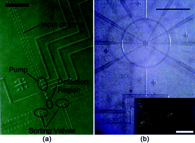 | ||
| Fig. 8 PDMS microfluidic devices with integrated pumps and values. (a) A PDMS microfluidic cell sorter. (b) A microfluidic rotary pump. The material enters via the channel at the bottom, and is circulated by the pneumatically actuated pumping lines. Inset: image showing directed motion of fluorescent beads along the microfluidic channel. Note: color in images is not intrinsic to the device. Scale bar = 1 mm. Adapted by permission from AAAS: Science, ref. 158 © 2000. | ||
However, there are also several limitations of PDMS microfluidics that are inherent in the material properties. The minimum channel size is dependent on the flexibility of the PDMS. In order to make high performance pumps and valves, the polymer must be flexible.155,158 However, this flexibility also can create channels that irreversibly collapse. Therefore, the minimum channel size is typically 10's of microns. Additionally, PDMS is slightly porous and can swell upon exposure to alcohols or extended exposure to common buffers and water. As all biological research takes place in water-based solutions, this effect limits the lifetime of the fluidic device.
More recent research efforts in the field of microfluidics have focused on increasing the density of the fluidic channels, creating 3-D fluidic channels and integrating the devices with sensing elements, such as waveguide sensors and micro-spectrometers.146,161,168 Several of the integrated sensor devices have also included elements of sample preparation, such as filters, enabling the possibility of serum and whole blood to be directly used in the sensor system.153,165
Parylene-based fluidic devices are typically fabricated in a clean room environment, and the sensor component is directly incorporated during the fluidic channel fabrication.169 Because parylene is not transparent over a wide range of wavelengths, it is difficult to integrate with fluorescent optical microscopy methods. However, it has been very successfully integrated with mechanical, electrical and label-free optical techniques.147,162,169
For example, recent results have demonstrated the ability to integrate MEMs sensors with parylene microfluidics.169 Using this type of integrated device, changes in cellular behavior in response to fluid shear stress were detected by monitoring the change in the mechanical properties of the cell. This type of quantitative measurement in a highly controlled environment was very difficult to perform before parylene microfluidic devices were developed.
4.2 Nanofluidic devices
As sensing elements transition from micro- to nano-scale devices, it becomes possible to create very dense arrays of sensors. At this point, the limiting size and scale factor becomes the density of the sample delivery method. Therefore, there is increased pressure for the microfluidic channel size to match that of the sensor. This push has created the new, emerging field of nanofluidics.However, one of the primary hurdles in this area is creating devices with functionality, like dynamically controlled mixing and sorting. Because the silica channel is rigid, it is very difficult to integrate mixing and pumping mechanisms on-chip with complex samples which contain components with similar properties.173–175
Recent work in this area is investigating the use of combining both electrophoretic and thermophoretic sample separation and sorting.173–176 Previous silica devices had focused solely on leveraging the difference in charge of various biological molecules to perform sample filtering. However, by combining the electrophoretic and thermophoretic mechanisms, it is possible to improve the isolation of the component of interest, thereby potentially improving the signal:noise and false-positive and false-negative ratios of the sensor.
Unlike all of the other devices discussed thus far, silicon devices are not completely transparent, restricting the range of potential applications. Additionally, as silicon is very hydrophobic, additional consideration must be given to developing an appropriate surface functionalization to change this property to enable medium to low pressure fluid flow. The incorporation of additional functionality, such as mixers and pumps, must be accomplished using methods similar to the parylene and glass devices.
However, because many of the integrated optical detection methods discussed in the previous sections are fabricated on silicon substrates, the integration of these sensors with silicon-based fluidic channels is straightforward. One example of such an integrated device was recently demonstrated by the research group of Altug at Boston University. In this integrated system, a surface plasmon sensor was integrated with 3-D silicon fluidic channel to improve the sample delivery and reduce the dead volume of the sensor system.183
5 Future outlook and conclusions
The label-free sensing methods discussed in the present review form a toolbox of techniques that can be used by the biotechnologist and that enable numerous experiments and biochemical investigations. Furthermore, the addition of surface specificity to these devices broadens the range of biochemical molecules and pathways that can be investigated, resulting in an almost limitless arena for the discovery and understanding of biochemical interactions. Currently, however, the majority of these devices operate in isolation, forcing researchers to choose between mechanical, optical, or electrical transduction methods. Therefore, a common question asked by biotechnologists is “which method is best”?To eliminate the need for this question, researchers are currently developing multi-modality techniques which combine different surface functionalization chemistries and transduction mechanisms, as well as extending the working range of the transducers from the single molecule level to high concentration. Therefore, although it is unlikely that there will ever be a single, perfect sensor, we can envision the creation of a sensing unit comprised of arrays of numerous devices, with varying transduction methods and specificities, that is capable of capturing the behavior or signal of interest.
Additionally, current research in the area of sample collection and delivery for various types of sensors complements the work done in the areas of sensor development. For instance, by improving the sample collection and delivery methods, it will be possible to relax tolerances on sensor performance, potentially enabling less expensive technology to be used for the given application. While many sensors have already been integrated with microfluidic delivery systems and have seen an improvement in performance as a result, some have yet to make this transition.21 By developing and implementing sample delivery and re-circulation systems, many sensors will improve their detection capabilities.
Lastly, while the development of transduction methods and surface functionalization techniques will have an obvious impact in the areas of detection for military, medical, and environmental diagnostics, it also offers the opportunity to explore new areas that can provide insight and understanding into biological processes. For example, the development of environmentally stable binding sites is a very active area of research, not just for sensors, but also for therapeutics. Using these transduction methods to study, for example, the binding interactions of proteins and ligands could lead to an improved understanding of the structure–function relationship of proteins, which could lead to the development of new protocols for drug development, as well as libraries of binding sites for specific biomolecules, diagnostic type, and environmental survival ability. Alternatively, investigation into sensor material could yield great insight into the relationships between sensor structure, material properties, and detection ability. It is therefore unsurprising that the remarkable breadth and depth of applications for the transduction methods reviewed in this report have created a rich and evolving field of great impact on science and technology.
Acknowledgements
The authors would like to thank Professor Mark Thompson and Professor Chongwu Zhou at the University of Southern California, Professor David Erickson at Cornell University, Professor Yeshaiahu Fainman at the University of California San Diego, Heather McCaig and Professor Nate Lewis at the California Institute of Technology, and Dr Richard Cote and Dr Ram Datar at the University of Miami for authorizing use of figures and images included in this article and in the table of contents image. This review was supported by the National Science Foundation [0852581], the Army Research Lab [W911NF-09-0041], and the ONR Young Investigator Program. Funding was also provided by the USC Women in Science and Engineering program. Additional information can be found at: http://armani.usc.edu/.Notes and references
- Y. S. Bae, S. W. Kang, M. S. Seo, I. C. Baines, E. Tekle, P. B. Chock and S. G. Rhee, J. Biol. Chem., 1997, 272, 217–221 CrossRef CAS.
- T. Balla, J. Cell Sci., 2005, 118, 2093–2104 CrossRef CAS.
- A. Camilli and B. L. Bassler, Science, 2006, 311, 1113–1116 CrossRef CAS.
- L. C. Cantley, Science, 2002, 296, 1655–1657 CrossRef CAS.
- G. Di Paolo and P. De Camilli, Nature, 2006, 443, 651–657 CrossRef CAS.
- D. V. Faller, Clin. Exp. Pharmacol. Physiol., 1999, 26, 74–84 CrossRef CAS.
- D. Vaudry, P. J. S. Stork, P. Lazarovici and L. E. Eiden, Science, 2002, 296, 1648–1649 CrossRef CAS.
- R. L. Silverstein and M. Febbraio, Sci. Signaling, 2009, 2, re3 CrossRef.
- A. K. Mustafa, M. M. Gadalla and S. H. Snyder, Sci. Signaling, 2009, 2, re2 CrossRef.
- Y. Cao, Sci. Signaling, 2009, 2, re1 CrossRef.
- A. Schwegmann and F. Brombacher, Sci. Signaling, 2008, 1, re8 CrossRef.
- R. A. Harris, J. R. Trudell and S. J. Mihic, Sci. Signaling, 2008, 1, re7 CrossRef.
- A. H. Guse and H. C. Lee, Sci. Signaling, 2008, 1, re10 CrossRef.
- M. B. Major and R. T. Moon, Sci. Signaling, 2009, 2, eg7 CrossRef.
- R. Cheong, C. J. Wang and A. Levchenko, Sci. Signaling, 2009, 2, pl2 CrossRef.
- C. M. Franz, A. Taubenberger, P.-H. Puech and D. J. Muller, Science's STKE, 2007, 2007, pl5 Search PubMed.
- A. C. von Philipsborn, S. Lang, Z. Jiang, F. Bonhoeffer and M. Bastmeyer, Science's STKE, 2007, 2007, pl6 Search PubMed.
- M. Kodiha, C. M. Brown and U. Stochaj, Sci. Signaling, 2008, 1, pl2 CrossRef.
- S. Jalal, R. Arsenault, A. A. Potter, L. A. Babiuk, P. J. Griebel and S. Napper, Sci. Signaling, 2009, 2, pl1 CrossRef.
- X. D. Fan, I. M. White, S. I. Shopoua, H. Y. Zhu, J. D. Suter and Y. Z. Sun, Anal. Chim. Acta, 2008, 620, 8–26 CrossRef CAS.
- C. Monat, P. Domachuk and B. J. Eggleton, Nat. Photonics, 2007, 1, 106–114 Search PubMed.
- R. Horvath, H. C. Pedersen, N. Skivesen, D. Selmeczi and N. B. Larsen, Opt. Lett., 2003, 28, 1233–1235 Search PubMed.
- P. Dumais, C. L. Callender, J. P. Noad and C. J. Ledderhof, IEEE Photonics Technol. Lett., 2005, 17, 441–443 CrossRef CAS.
- F. Sundberg and R. Karlsson, Immunology, 2007, 120, 46–47 CrossRef.
- G. F. Zheng, F. Patolsky, Y. Cui, W. U. Wang and C. M. Lieber, Nat. Biotechnol., 2005, 23, 1294–1301 CrossRef CAS.
- R. G. Knobel and A. N. Cleland, Nature, 2003, 424, 291–293 CrossRef CAS.
- T. P. Burg, M. Godin, S. M. Knudsen, W. Shen, G. Carlson, J. S. Foster, K. Babcock and S. R. Manalis, Nature, 2007, 446, 1066–1069 CrossRef CAS.
- B. Huang, H. K. Wu, D. Bhaya, A. Grossman, S. Granier, B. K. Kobilka and R. N. Zare, Science, 2007, 315, 81–84 CrossRef CAS.
- X. L. Sun, C. L. Stabler, C. S. Cazalis and E. L. Chaikof, Bioconjugate Chem., 2006, 17, 52–57 CrossRef CAS.
- R. A. Vijayendran and D. E. Leckband, Anal. Chem., 2001, 73, 471–480 CrossRef CAS.
- B. M. Kihlberg, U. Sjobring, W. Kastern and L. Bjorck, J. Biol. Chem., 1992, 267, 25583–25588 CAS.
- J. C. McDonald, D. C. Duffy, J. R. Anderson, D. T. Chiu, H. K. Wu, O. J. A. Schueller and G. M. Whitesides, Electrophoresis, 2000, 21, 27–40 CrossRef CAS.
- R. Michel, I. Reviakine, D. Sutherland, C. Fokas, G. Csucs, G. Danuser, N. D. Spencer and M. Textor, Langmuir, 2002, 18, 8580–8586 CrossRef CAS.
- C. Neils, Z. Tyree, B. Finlayson and A. Folch, Lab Chip, 2004, 4, 342–350 RSC.
- T. Thorsen, S. J. Maerkl and S. R. Quake, Science, 2002, 298, 580–584 CrossRef CAS.
- J. Fraden, Handbook of Modern Sensor: Physics, Designs, and Applications, Springer, 3rd edn, 2003 Search PubMed.
- S. D. Senturia, Microsystem Design, Springer, 2004 Search PubMed.
- J. Carrano, Chemical and Biological Sensor Standards Study, DARPA, Washington, DC 2005 Search PubMed.
- D. Erickson, S. Mandal, A. H. J. Yang and B. Cordovez, Microfluid. Nanofluid., 2008, 4, 33–52 CrossRef CAS.
- R. Datar, S. Kim, S. Jeon, P. Hesketh, S. Manalis, A. Boisen and T. Thundat, MRS Bull., 2009, 34, 449–454 CAS.
- J. B. Heng, C. Ho, T. Kim, R. Timp, A. Aksimentiev, Y. V. Grinkova, S. Sligar, K. Schulten and G. Timp, Biophys. J., 2004, 87, 2905–2911 CrossRef CAS.
- O. Aksimentiev, Nanoscale, 2010, 2, 468–483 RSC.
- K. S. Kim, H.-S. Lee, J.-A. Yang, M.-H. Jo and S. K. Hahn, Nanotechnology, 2009, 20, 235501 CrossRef.
- F. Patolsky, G. F. Zheng, O. Hayden, M. Lakadamyali, X. W. Zhuang and C. M. Lieber, Proc. Natl. Acad. Sci. U. S. A., 2004, 101, 14017–14022 CrossRef CAS.
- F. Patolsky, G. F. Zheng and C. M. Lieber, Nat. Protoc., 2006, 1, 1711–1724 Search PubMed.
- F. N. Ishikawa, H. K. Chang, M. Curreli, H. I. Liao, C. A. Olson, P. C. Chen, R. Zhang, R. W. Roberts, R. Sun, R. J. Cote, M. E. Thompson and C. W. Zhou, ACS Nano, 2009, 3, 1219–1224 CrossRef CAS.
- J. E. Barrick, T. T. Takahashi, A. Balakin and R. W. Roberts, Methods, 2001, 23, 287–293 CrossRef CAS.
- J. E. Barrick, T. T. Takahashi, J. S. Ren, T. B. Xia and R. W. Roberts, Proc. Natl. Acad. Sci. U. S. A., 2001, 98, 12374–12378 CrossRef CAS.
- H. I. Liao, C. A. Olson, S. M. Hwang, H. Y. Deng, E. Wong, R. S. Baric, R. W. Roberts and R. Sun, J. Biol. Chem., 2009, 284, 17512–17520 CrossRef CAS.
- T. T. Takahashi, R. J. Austin and R. W. Roberts, Trends Biochem. Sci., 2003, 28, 159–165 CrossRef CAS.
- M. Yue, J. C. Stachowiak, H. Lin, R. Datar, R. Cote and A. Majumdar, Nano Lett., 2008, 8, 520–524 CrossRef CAS.
- K. M. Hansen, H. F. Ji, G. H. Wu, R. Datar, R. Cote, A. Majumdar and T. Thundat, Anal. Chem., 2001, 73, 1567–1571 CrossRef.
- G. H. Wu, H. F. Ji, K. Hansen, T. Thundat, R. Datar, R. Cote, M. F. Hagan, A. K. Chakraborty and A. Majumdar, Proc. Natl. Acad. Sci. U. S. A., 2001, 98, 1560–1564 CrossRef CAS.
- G. H. Wu, R. H. Datar, K. M. Hansen, T. Thundat, R. J. Cote and A. Majumdar, Nat. Biotechnol., 2001, 19, 856–860 CrossRef CAS.
- N. J. Harrick, Internal Reflection Spectroscopy, John Wiley and Sons, New York, 1967 Search PubMed.
- J. Fahrenfort, Spectrochim. Acta, 1961, 17, 698–709 CrossRef CAS.
- G. Rong, A. Najmaie, J. E. Sipe and S. M. Weiss, Biosens. Bioelectron., 2008, 23, 1572–1576 CrossRef CAS.
- A. M. Armani, R. P. Kulkarni, S. E. Fraser, R. C. Flagan and K. J. Vahala, Science, 2007, 317, 783–787 CrossRef CAS.
- F. Vollmer and S. Arnold, Nat. Methods, 2008, 5, 591–596 CrossRef CAS.
- D. Derickson, Fiber Optic Test and Measurement, Prentice Hall, 1997 Search PubMed.
- B. E. A. Saleh and M. C. Teich, Fundamentals of Photonics, Wiley-Interscience, 2nd edn, 2007 Search PubMed.
- A. Politi, M. J. Cryan, J. G. Rarity, S. Yu and J. L. O'Brien, Science, 2008, 320, 646–649 CrossRef CAS.
- J. Xu, D. Suarez and D. S. Gottfried, Anal. Bioanal. Chem., 2007, 389, 1193–1199 CrossRef CAS.
- G. M. Hale and M. R. Querry, Appl. Opt., 1973, 12, 555–563 CAS.
- M. L. Gorodetsky, A. A. Savchenkov and V. S. Ilchenko, Opt. Lett., 1996, 21, 453–455 Search PubMed.
- D. W. Vernooy, V. S. Ilchenko, H. Mabuchi, E. W. Streed and H. J. Kimble, Opt. Lett., 1998, 23, 247–249 Search PubMed.
- S. Mookherjea and A. Yariv, IEEE J. Sel. Top. Quantum Electron., 2002, 8, 448–456 CrossRef CAS.
- X. Zhang, H.-S. Choi and A. M. Armani, Appl. Phys. Lett., 2010, 96, 153304 CrossRef.
- G. Anetsberger, R. Riviere, A. Schliesser, O. Arcizet and T. J. Kippenberg, Nat. Photonics, 2008, 2, 627–633 Search PubMed.
- A. Di Virgilio, L. Barsotti, S. Braccini, C. Bradaschia, G. Cella, C. Corda, V. Dattilo, I. Ferrante, F. Fidecaro, I. Fiori, F. Frasconi, A. Gennai, A. Giazotto, P. La Penna, G. Losurdo, E. Majorana, M. Mantovani, A. Pasqualetti, D. Passuello, F. Piergiovanni, A. Porzio, P. Puppo, P. Rapagnani, F. Ricci, S. Solimeno, G. Vajente and F. Vetrano, Phys. Rev. A: At., Mol., Opt. Phys., 2006, 74, 013813 CrossRef.
- I. Favero and K. Karrai, Nat. Photonics, 2009, 3, 201–205 Search PubMed.
- J. E. Heebner and R. W. Boyd, J. Mod. Opt., 2002, 49, 2629–2636 CrossRef.
- P. Rabiei and W. H. Steier, IEEE Photonics Technol. Lett., 2003, 15, 1255–1257 CrossRef.
- H. C. Ren, F. Vollmer, S. Arnold and A. Libchaber, Opt. Express, 2007, 15, 17410–17423 CrossRef.
- K. Srinivasan, P. E. Barclay and O. Painter, Phys. Status Solidi B, 2005, 242, 1187–1191 CrossRef CAS.
- J. D. Suter, I. M. White, H. Zhu, H. Shi, C. W. Caldwell and X. Fan, Biosens. Bioelectron., 2008, 23, 1003–1009 CrossRef CAS.
- Q. F. Xu and M. Lipson, Opt. Express, 2007, 15, 924–929 CrossRef.
- T. Aoki, B. Dayan, E. Wilcut, W. P. Bowen, A. S. Parkins, T. J. Kippenberg, K. J. Vahala and H. J. Kimble, Nature, 2006, 443, 671–674 CrossRef CAS.
- S. Mookherjea and A. Oh, Opt. Lett., 2007, 32, 289–291 Search PubMed.
- S. Mookherjea and M. A. Schneider, Opt. Express, 2008, 16, 15130–15136 CrossRef.
- S. Mandal, J. M. Goddard and D. Erickson, Lab Chip, 2009, 9, 2924–2932 RSC.
- S. M. Spillane, T. J. Kippenberg, O. J. Painter and K. J. Vahala, Phys. Rev. Lett., 2003, 91, 043902 CrossRef CAS.
- M. Cai and K. Vahala, Opt. Lett., 2001, 26, 884–886 Search PubMed.
- C. Y. Chao and L. J. Guo, Appl. Phys. Lett., 2003, 83, 1527–1529 CrossRef CAS.
- A. M. Armani and K. J. Vahala, Opt. Lett., 2006, 31, 1896–1898 Search PubMed.
- C. Monat, P. Domachuk and B. J. Eggleton, Nat. Photonics, 2006, 1, 106–114 Search PubMed.
- E. Krioukov, D. J. W. Klunder, A. Driessen, J. Dreve and C. Otto, Opt. Lett., 2002, 27, 512–514 Search PubMed.
- A. Ksendzov and Y. Lin, Opt. Lett., 2005, 30, 3344–3346 Search PubMed.
- R. W. Boyd and J. E. Heebner, Appl. Opt., 2001, 40, 5742–5747 CrossRef CAS.
- S. Blair and Y. Chen, Appl. Opt., 2001, 40, 570–582 CrossRef CAS.
- V. S. Ilchenko and L. Maleki, in Laser Resonators IV, ed. A. V. Kudryashov and A. H. Paxton, Proceedings of the SPIE, 2001, vol. 4270, pp. 120–130 Search PubMed.
- J. L. Nadeau, V. S. Iltchenko, D. Kossakovski, G. H. Bearman and L. Maleki, in Laser Resonators and Beam Control V, ed. A. V. Kudryashov, Proceedings of the SPIE, 2002, vol. 4629, pp. 172–180 Search PubMed.
- S. Mandal and D. Erickson, Conference on Lasers & Electro-Optics/Quantum Electronics and Laser Science Conference (Cleo/Qels 2007), 2007, vol. 1–5, pp. 311–312, 2796 Search PubMed.
- J. G. Zhu, S. K. Ozdemir, Y. F. Xiao, L. Li, L. N. He, D. R. Chen and L. Yang, Nat. Photonics, 2010, 4, 46–49 Search PubMed.
- F. Vollmer, S. Arnold and D. Keng, Proc. Natl. Acad. Sci. U. S. A., 2008, 105, 20701–20704 CrossRef CAS.
- Y. Akahane, T. Asano, B. S. Song and S. Noda, Nature, 2003, 425, 944–947 CrossRef CAS.
- B. S. Song, S. Noda, T. Asano and Y. Akahane, Nat. Mater., 2005, 4, 207–210 CrossRef CAS.
- M. Lee and P. M. Fauchet, Opt. Express, 2007, 15, 4530–4535 CrossRef CAS.
- S. Mandal and D. Erickson, Opt. Express, 2008, 16, 1623–1631 CrossRef.
- J. Homola, I. Koudela and S. S. Yee, Sens. Actuators, B, 1999, 54, 16–24 CrossRef.
- J. Homola, S. S. Yee and G. Gauglitz, Sens. Actuators, B, 1999, 54, 3–15 CrossRef.
- A. J. Haes, S. L. Zou, G. C. Schatz and R. P. Van Duyne, J. Phys. Chem. B, 2004, 108, 109–116 CrossRef CAS.
- A. J. Haes, S. L. Zou, G. C. Schatz and R. P. Van Duyne, J. Phys. Chem. B, 2004, 108, 6961–6968 CrossRef CAS.
- A. J. Haes and R. P. Van Duyne, Plasmonics: Metallic Nanostructures and their Optical Properties, Proceedings of the SPIE, 2003, vol. 5221, pp. 47–58 Search PubMed.
- K. A. Tetz, L. Pang and Y. Fainman, Opt. Lett., 2006, 31, 1528–1530 CrossRef.
- L. Pang, H. M. P. Chen, L. L. Wang, J. M. Beechem and Y. Fainman, Opt. Express, 2009, 17, 14700–14709 CrossRef CAS.
- X. S. Jiang, D. Y. Li, X. Xu, Y. B. Ying, Y. B. Li, Z. Z. Ye and J. P. Wang, Biosens. Bioelectron., 2008, 23, 1577–1587 CrossRef CAS.
- P. B. Luppa, L. J. Sokoll and D. W. Chan, Clin. Chim. Acta, 2001, 314, 1–26 CrossRef CAS.
- M. Y. Wei and L. H. Guo, Prog. Chem. (Beijing, China), 2009, 21, 492–502 Search PubMed.
- C. A. K. Borrebaeck, Immunol. Today, 2000, 21, 379–382 CrossRef CAS.
- E. Soderlind, M. Ohlin and R. Carlsson, Immunotechnology, 1999, 4, 279–285 CrossRef CAS.
- A. Amine, H. Mohammadi, I. Bourais and G. Palleschi, Biosens. Bioelectron., 2006, 21, 1405–1423 CrossRef CAS.
- D. R. Shankaran, K. V. A. Gobi and N. Miura, Sens. Actuators, B, 2007, 121, 158–177 CrossRef.
- K. Hegnerova, M. Bockova, H. Vaisocherova, Z. Kristofikova, J. Ricny, D. Ripova and J. Homola, Sens. Actuators, B, 2009, 139, 69–73 CrossRef.
- L. Zanoli, R. D'Agata and G. Spoto, Minerva Biotechnol, 2008, 20, 165–174 Search PubMed.
- O. R. Bolduc, C. M. Clouthier, J. N. Pelletier and J. F. Masson, Anal. Chem., 2009, 81, 6779–6788 CrossRef CAS.
- K. V. Gobi, H. Iwasaka and N. Miura, Biosens. Bioelectron., 2007, 22, 1382–1389 CrossRef CAS.
- K. V. Gobi, S. J. Kim, H. Tanaka, Y. Shoyama and N. Miura, Sens. Actuators, B, 2007, 123, 583–593 CrossRef.
- J. K. Zhang, S. M. Dong, J. H. Lu, A. P. F. Turner, Q. J. Fan, S. R. Jia, H. J. Yang, C. S. Qiao, H. Zhou and G. W. He, Anal. Lett., 2009, 42, 2905–2913 CrossRef CAS.
- M. Lee and D. R. Walt, Anal. Biochem., 2000, 282, 142–146 CrossRef CAS.
- S. H. Lee, H. J. Ko and T. H. Park, Biosens. Bioelectron., 2009, 25, 55–60 CrossRef.
- J. E. Dover, G. M. Hwang, E. H. Mullen, B. C. Prorok and S. J. Suh, J. Microbiol. Methods, 2009, 78, 10–19 CrossRef CAS.
- S. Kumbhat, D. R. Shankaran, S. J. Kim, K. V. Gobi, V. Joshi and N. Miura, Chem. Lett., 2006, 678–679 CrossRef CAS.
- S. Kumbhat, D. R. Shankaran, S. J. Kim, K. V. Gobi, V. Joshi and N. Miura, Biosens. Bioelectron., 2007, 23, 421–427 CrossRef CAS.
- S. Subrahmanyam, S. A. Piletsky and A. P. F. Turner, Anal. Chem., 2002, 74, 3942–3951 CrossRef CAS.
- T. C. Chou, J. Rick and Y. C. Weng, 7th IEEE Conference on Nanotechnology, 2007, vol. 1–3, pp. 16–20 Search PubMed.
- T. H. Nguyen and R. J. Ansell, Org. Biomol. Chem., 2009, 7, 1211–1220 RSC.
- A. Rehman, N. Iqbal, P. A. Lieberzeit and F. L. Dickert, Monatsh. Chem., 2009, 140, 931–939 CrossRef CAS.
- Q. Y. Yang, Q. Sun, T. S. Zhou, G. Y. Shi and L. T. Jin, J. Agric. Food Chem., 2009, 57, 6558–6563 CrossRef CAS.
- C. Alexander, H. S. Andersson, L. I. Andersson, R. J. Ansell, N. Kirsch, I. A. Nicholls, J. O'Mahony and M. J. Whitcombe, J. Mol. Recognit., 2006, 19, 106–180 CrossRef.
- L. Ye and K. Mosbach, Chem. Mater., 2008, 20, 859–868 CrossRef CAS.
- B. Hock, Anal. Chim. Acta, 1997, 347, 177–186 CrossRef CAS.
- N. Miura, M. Sasaki, K. V. Gobi, C. Kataoka and Y. Shoyama, Biosens. Bioelectron., 2003, 18, 953–959 CrossRef CAS.
- V. Chechik, R. M. Crooks and C. J. M. Stirling, Adv. Mater., 2000, 12, 1161–1171 CrossRef CAS.
- A. Ulman, Chem. Rev., 1996, 96, 1533–1554 CrossRef CAS.
- S. R. Wasserman, Y. T. Tao and G. M. Whitesides, Langmuir, 1989, 5, 1074–1087 CrossRef CAS.
- J. W. Lee, S. J. Sim, S. M. Cho and J. Lee, Biosens. Bioelectron., 2005, 20, 1422–1427 CrossRef CAS.
- S. S. Mark, N. Sandhyarani, C. C. Zhu, C. Campagnolo and C. A. Batt, Langmuir, 2004, 20, 6808–6817 CrossRef CAS.
- T. Kaiser, P. Gudat, W. Stock, G. Pappert, M. Grol, D. Neumeier and P. B. Luppa, Anal. Biochem., 2000, 282, 173–185 CrossRef CAS.
- S. Andras, N. Adanyi, I. Szekacs, K. Majer-Baranyi and S. Istvan, Appl. Opt., 2009, 48, B151–B158 CrossRef.
- T. Nagel, E. Ehrentreich-Forster, M. Singh, K. Schmitt, A. Brandenburg, A. Berka and F. F. Bier, Sens. Actuators, B, 2008, 129, 934–940 CrossRef.
- B. S. Sumerlin and A. P. Vogt, Macromolecules, 2009, 43, 1–13.
- J. Kalia and R. T. Raines, Curr. Org. Chem., 2010, 14, 138–147 CrossRef CAS.
- D. Knopp, D. P. Tang and R. Niessner, Anal. Chim. Acta, 2009, 647, 14–30 CrossRef CAS.
- Y. S. Chi, J. K. Lee, K. B. Lee, D. J. Kim and I. S. Choi, Bull. Korean Chem. Soc., 2005, 26, 361–370 CrossRef CAS.
- C. J. Choi, I. D. Block, B. Bole, D. Dralle and B. T. Cunningham, IEEE Sens. J., 2009, 9, 1697–1704 CrossRef.
- S. Zheng, H. Lin, J. Q. Liu, M. Balic, R. Datar, R. J. Cote and Y. C. Tai, J. Chromatogr., A, 2007, 1162, 154–161 CrossRef CAS.
- P. Svarnas, A. Plecis, C. Nanteuil, D. Duong, C. David, M. Muller and Y. Chen, Eur. Phys. J.: Appl. Phys., 2008, 44, 245–253 CrossRef CAS.
- D. T. Chiu, E. Pezzoli, H. K. Wu, A. D. Stroock and G. M. Whitesides, Proc. Natl. Acad. Sci. U. S. A., 2001, 98, 2961–2966 CrossRef CAS.
- S. K. Sia and G. M. Whitesides, Electrophoresis, 2003, 24, 3563–3576 CrossRef CAS.
- G. M. Whitesides, Nature, 2006, 442, 368–373 CrossRef CAS.
- D. Pushkarev, N. F. Neff and S. R. Quake, Nat. Biotechnol., 2009, 27, 847–U101 CrossRef CAS.
- R. Gomez-Sjoberg, A. A. Leyrat, D. M. Pirone, C. S. Chen and S. R. Quake, Anal. Chem., 2007, 79, 8557–8563 CrossRef.
- A. Groisman, M. Enzelberger and S. R. Quake, Science, 2003, 300, 955–958 CrossRef CAS.
- T. M. Squires and S. R. Quake, Rev. Mod. Phys., 2005, 77, 977–1026 CrossRef CAS.
- R. F. Ismagilov, D. Rosmarin, P. J. A. Kenis, D. T. Chiu, W. Zhang, H. A. Stone and G. M. Whitesides, Anal. Chem., 2001, 73, 4682–4687 CrossRef CAS.
- A. D. Stroock, S. K. W. Dertinger, A. Ajdari, I. Mezic, H. A. Stone and G. M. Whitesides, Science, 2002, 295, 647–651 CrossRef CAS.
- S. R. Quake and A. Scherer, Science, 2000, 290, 1536–1540 CrossRef CAS.
- Y. Marcy, T. Ishoey, R. S. Lasken, T. B. Stockwell, B. P. Walenz, A. L. Halpern, K. Y. Beeson, S. M. D. Goldberg and S. R. Quake, PLoS Genet., 2007, 3, 1702–1708 Search PubMed.
- R. Mendis, V. Astley, J. B. Liu and D. M. Mittleman, Appl. Phys. Lett., 2009, 95, 171113 CrossRef.
- V. Maselli, J. R. Grenier, S. Ho and P. R. Herman, Opt. Express, 2009, 17, 11719–11729 CrossRef CAS.
- M. Rouhanizadeh, G. Soundararajan, R. Lo, D. Arcas, F. K. Browand and T. K. Hsiai, IEEE Sens. J., 2006, 6, 78–88 CrossRef.
- H. S. Noh, Y. Huang and P. J. Hesketh, Sens. Actuators, B, 2004, 102, 78–85 CrossRef.
- D. B. Weibel, W. R. DiLuzio and G. M. Whitesides, Nat. Rev. Microbiol., 2007, 5, 209–218 Search PubMed.
- E. P. Kartalov, J. F. Zhong, A. Scherer, S. R. Quake, C. R. Taylor and W. F. Anderson, BioTechniques, 2006, 40, 85–90 CrossRef CAS.
- C. L. Hansen, E. Skordalakes, J. M. Berger and S. R. Quake, Proc. Natl. Acad. Sci. U. S. A., 2002, 99, 16531–16536 CrossRef CAS.
- S. R. Bates and S. R. Quake, Appl. Phys. Lett., 2009, 95, 073705 CrossRef.
- C. F. Carlborg, K. B. Gylfason, A. Kazmierczak, F. Dortu, M. J. B. Polo, A. M. Catala, G. M. Kresbach, H. Sohlstrom, T. Moh, L. Vivien, J. Popplewell, G. Ronan, C. A. Barrios, G. Stemme and W. van der Wijngaart, Lab Chip, 2010, 10, 281–290 RSC.
- M. Rouhanizadeh, W. Takabe, L. S. Ai, H. Y. Yu and T. Hsiai, in Nitric Oxide, Pt G: Oxidative and Nitrosative Stress in Redox Regulation of Cell Signaling, ed. E. Cadena and L. Parker, Elsevier Academic Press Inc., 2008, vol. 441, pp. 111–150 Search PubMed.
- Q. H. He and S. A. Chen, Prog. Chem. (Beijing, China), 2008, 20, 2061–2067 Search PubMed.
- B. Renberg, K. Sato, T. Tsukahara, K. Mawatari and T. Kitamori, Microchim. Acta, 2009, 166, 177–181 CrossRef CAS.
- T. Maleki, S. Mohammadi and B. Ziaie, Nanotechnology, 2009, 20, 105302 CrossRef CAS.
- W. Sparreboom, A. van den Berg and J. C. T. Eijkel, Nat. Nanotechnol., 2009, 4, 713–720 CrossRef CAS.
- V. N. Phan, C. Yang and N. T. Nguyen, Microfluid. Nanofluid., 2009, 7, 519–530 CrossRef CAS.
- Y. J. Oh, A. L. Garcia, D. N. Petsev, G. P. Lopez, S. R. J. Brueck, C. F. Ivory and S. M. Han, Lab Chip, 2009, 9, 1601–1608 RSC.
- Y. S. Choi and S. J. Kim, J. Colloid Interface Sci., 2009, 333, 672–678 CrossRef CAS.
- S. M. Stavis, E. A. Strychalski and M. Gaitan, Nanotechnology, 2009, 20, 165302 CrossRef.
- S. K. Kim, H. Cho, H. K. Park, J. H. Kim and B. H. Chung, J. Nanosci. Nanotechnol., 2010, 10, 637–642 CrossRef CAS.
- A. P. Han, N. F. de Rooij and U. Staufer, Nanotechnology, 2006, 17, 2498–2503 CrossRef CAS.
- Q. F. Xia, K. J. Morton, R. H. Austin and S. Y. Chou, Nano Lett., 2008, 8, 3830–3833 CrossRef CAS.
- Q. F. Xia and S. Y. Chou, Appl. Phys. A: Mater. Sci. Process., 2010, 98, 9–59 CrossRef CAS.
- D. Stein, F. H. J. van der Heyden, W. J. A. Koopmans and C. Dekker, Proc. Natl. Acad. Sci. U. S. A., 2006, 103, 15853–15858 CrossRef CAS.
- A. A. Yanik, M. Huang, A. Artar, T. Y. Chang and H. Altug, Appl. Phys. Lett., 2010, 96, 021101 CrossRef.
- J. Zhang, H. P. Lang, F. Huber, A. Bietsch, W. Grange, U. Certa, R. McKendry, H. J. Guntgerodt, M. Hegner and C. Gerber, Nat. Nanotechnol., 2006, 1, 214–220 CrossRef CAS.
- J. Xu, D. Suarez and D. S. Gottfried, Anal. Bioanal. Chem., 2007, 389, 1193–1199 CrossRef CAS.
- D. K. Armani, T. J. Kippenberg, S. M. Spillane and K. J. Vahala, Nature, 2003, 421, 925–928 CrossRef CAS.
- C. Y. Chao and L. J. Guo, J. Vac. Sci. Technol., B, 2002, 20, 2862–2866 CrossRef CAS.
| This journal is © The Royal Society of Chemistry 2010 |