Single light-emitting polymer nanofiber field-effect transistors
Deyu
Tu
a,
Stefano
Pagliara
ab,
Andrea
Camposeo
a,
Luana
Persano
a,
Roberto
Cingolani
ac and
Dario
Pisignano
*abd
aNNL, National Nanotechnology Laboratory of CNR-Istituto Nanoscienze, Università del Salento,
via Arnesano, I-73100, Lecce, Italy. E-mail: Dario.pisignano@unisalento.it; Fax: +39 0832298146; Tel: +39 0832298146
bUniversità del Salento,
via Arnesano, I-73100, Lecce, Italy
cIstituto Italiano di Tecnologia (I.I.T.),
via Morego 30, I-16163, Genova, Italy
dIstituto Italiano di Tecnologia (I.I.T.), Center for Biomolecular Nanotechnologies,
via Barsanti 1, I-73010, Arnesano, LE, Italy
First published on 9th September 2010
Abstract
We report on single nanofiber field-effect transistors made by the light-emitting polymer, poly(2-methoxy-5-(2-ethylhexoxy)-1,4-phenylenevinylene). We measure electrical performances comparable to or better than those of thin-film transistors by the same organic semiconductor, due to the molecular alignment induced by electrospinning, such as hole mobility of the order of 10−3 cm2 V−1 s−1 and on/off current ratios up to 780. In addition, we observe controllable photoluminescence intensity quenching by varying the gate voltage up to −40 V with device operation in the luministor mode. Single light-emitting polymer nanofiber transistors coupling electrical and optical functionalities open the way towards low cost and flexible one-dimensional switches and nanofiber-based light-emitting transistors.
Introduction
One-dimensional (1D) semiconductor nanostructures attract growing interest in basic investigations of confinement effects on electronic and optical properties, and potential device applications.1 Inorganic nanowires2 and nanotubes3 are widely explored for their excellent carrier mobilities and high supported currents. On the other hand, 1D organic nanostructures are very promising because of their remarkable mechanical flexibility, cheapness, and tunable functionality. They are especially intriguing in view of their application as active channels in field-effect transistors (FETs) with reduced size and cost, and increased component density.4 FETs based on organic nanowires and nanofibers are particularly suitable for fundamental studies of the conduction and assembly properties of polymers in 1D nanostructures, and can be realized easily by solution processing methods, with applications ranging from electronic textiles to bio-chemical sensors.5 Polymer nanowire and fibers can be realized by various approaches, such as polymerization in nanoporous templates,6 self-assembly,7 soft lithographies,8 and electrospinning (ES).4,9Among these, ES is the simplest and highest-throughput technology, being based on the plastic stretching of a polymer solution by means of an applied voltage (1–50 kV on ∼10 cm). The stretching finally leads to the formation of fibers of sub-μm diameter. In particular, ES has been recently applied to light-emitting conjugated polymers such as poly(phenylenevinylene) (PPV) derivatives,10 which are strategic for the realization of many optoelectronic devices including light-emitting transistors.11 However, though exploited to fabricate single nanofiber transistors with semiconductor compounds such as the poly(3-hexylthiophene) (P3HT),4 ES is still unexplored as a method to realize FETs based on single nanofibers by light-emitting polymers.
In fact, the ES of light-emitting polymers is still challenging, because of the poor solubility and viscoelastic behaviour of many conjugated compounds. For these reasons, the most of previous reports are based on blending or wrapping conjugated polymers with soluble, thermoplastic and electrically insulating materials.12 Other methods include the coupling with molecular sieves into composite structures,10 and the incorporation of light-emitting dyes in optically inert matrices.13
In this paper, we report on fully conjugated polymer electrospun fibers by the 2-methoxy-5-(2-ethylhexoxy)-1,4-phenylenevinylene (MEH-PPV, inset of Fig. 1a) as p-type FET semiconductor channels. We measure a maximum hole mobility of 5 × 10⁻³ cm2/Vs and a current on-off ratio (Ion/Ioff) up to about 780. We find that the intensity of photoluminescence (PL) from single fibers within FETs can be electrically modulated in a luministor mode, decreasing down by a factor of 1.5 upon varying the gate voltage (VGS) from 0 to −40 V.
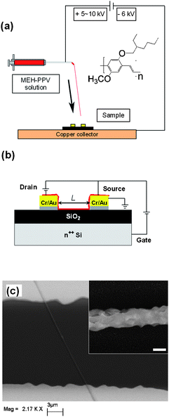 | ||
| Fig. 1 (a) Schematics of ES process to fabricate single nanofiber-based FETs. The arrow schematises the elongational direction of fiber extrusion, corresponding to the stretching direction during the deposition process. Inset: MEH-PPV molecular structure. (b) Schematics drawing of a single nanofiber FET in bottom-contact and back-gate configuration. L: inter-electrodes fiber length. (c) SEM micrograph of a typical device. Inset: Single nanofiber surface at high magnification. Marker = 200 nm. | ||
Experimental
Materials
Single-side polished n-type silicon (100) wafers with low resistivity (< 6 mΩ cm) and coated by thermally-grown SiO2 with thicknesses of 100 nm and 400 nm are by Silicon Materials, Landsberg am Lech, Germany. The light-emitting conjugated polymer, MEH-PPV, with average molecular weight (Mw) 750 000–1 250 000 is purchased from Sigma-Aldrich, St. Louis, MO, and dissolved in 0.016–0.027 mM chloroform solutions for ES.ES procedure and FET fabrication
The substrates for FET fabrication are carefully cleaned by ultrasonic baths in acetone and isopropanol for 5 min, followed by drying with N2. Cr/Au (with thickness 5 nm and 100 nm, respectively) source and drain electrodes, with a length of 200 μm and a width of 20 μm, are then defined by photolithography and metal lift-off processes. Au is commonly used as electrode material for hole injection into organics, whereas Cr is employed as underlying adhesion promoter.4,11 In addition, a thin layer of photoresist primer (hexamethyldisilizane, HMDS, Rohm and Haas Electronic Materials Ltd. Philadelphia, PA) is deposited on samples by spin-coating for 40 s at 4000 rpm to optimize the dielectric/organics interface.14 400–600 μL of the polymer solution is stored into a 1.0 mL plastic syringe tipped with a 27-gauge stainless steel needle, and injected at the end of the needle at a constant rate of 20 μL min−1 by a syringe pump (33 Dual Syringe Pump, Harvard Apparatus Inc., Holliston, MA). The positive lead from a high voltage supply (XRM30P, Gamma High Voltage Research Inc., Ormond Beach, FL) is connected to the metal needle applying a bias in the range of 5–10 kV over an inter-electrodes distance of about 10 cm, whereas the Si substrates with the defined Cr/Au microelectrodes are placed on a copper collector with an area of 10 × 10 cm2, on its turn biased at a negative voltage of −6 kV. Aligned arrays of fibers are obtained by using as collector a 1 mm-thick copper foil with a 2 mm rectangular gap. The foil is placed at about 10 cm from the needle and employed over a collection time of 103 s while rotating on a mandrel (RT Collector, Linari Engineering Srl) at 2500 rpm. All the ES experiments are performed in air at room temperature, with a humidity of 40–50%. Deposited fibers exhibit diameter between 100 nm and 1 μm, with an average value around 600 nm. Upon ES, devices are annealed in N2 at 90 °C for 60 min to remove residual solvent in polymer nanofibers and to enhance adhesion on the primer-treated SiO2 surface.SEM and AFM characterization
The morphology of single MEH-PPV nanofiber transistors is investigated by SEM using a Raith 150 electron-beam system operating with an acceleration voltage of 5 kV and an aperture size of 60 μm, and by AFM employing a Nanoscope IIIa controller with Multimode head, Veeco Instruments, Plainview, NY. Phosphorous-doped Si tips are employed with an 8–10 nm nominal curvature radius and a resonant frequency of 150 kHz.Electrical characterization
A probe station (PH100, Süss Micro Tec AG, Garching, Germany) and a stereomicroscope (MZ16FA, Leica Microsystems GmbH, Wetzlar, Germany) are used for electrically contacting the single MEH-PPV nanofiber transistors. The electrical characterization is carried out in air at room temperature and in dark, collecting and analyzing signals by means of a semiconductor parameter analyzer (4200 SCS, Keithley Instruments Inc. Cleveland, OH). The mean values reported are obtained by averaging over about 40 single light-emitting polymer nanofiber FETs fabricated and characterized in this study.Optical characterization
We perform fluorescence stereomicroscopy (MZ16 FA, Leica, Wetzlar, Germany) by exciting the samples with an Hg lamp (excitation wavelength in the range 470–490 nm) and spectrally selecting the emission through a long-pass emission filter (λ > 515 nm). The PL spectroscopy is performed by carefully coupling the luminescence signal from a nanofiber embedded in a FET device into a fiber-connected monochromator equipped with a charge coupled device detector (Ocean Optics, FL). To investigate the molecular organization in the light-emitting nanofibers, polarized PL spectroscopy is performed, exciting a single fiber by an Argon ion laser (λ = 476 nm) coupled to a 20× magnification objective of an inverted microscope and collecting emitted light with a polarization analyzer parallel (PL//) or perpendicular (PL⊥) to the fiber axis. The polarized emission spectra are corrected by the spectral response of the detection system. Fibers with diameters of a few μm are intentionally produced to collect polarized fluorescence micrographs. Polarized transmission Fourier transform infrared (FTIR) spectroscopy is carried out by exploiting a FTIR spectrophotometer (Spectrum 100, Perkin Elmer Inc.), equipped with a IR grid polarizer (consisting of 0.12 μm-wide strips of aluminium on a KRS-5 substrate, Specac Limited, UK) and by using a resolution of 4 cm−1. The 1.6 mm-wide beam incident orthogonally to the plane of the sample and it is polarized alternatively parallel or orthogonal to fibers aligned into arrays.Results and discussion
Electrospun nanofiber morphology
The ES deposition of light-emitting nanofibers on FET structures is schematized in Fig. 1a. n-Type Si wafers (Silicon Materials) are used both as device substrate and as back-gate electrode, and thermally-grown SiO2 is exploited as gate dielectric. Fibers are electrospun and collected as organic semiconductor channel onto the bottom-contact FETs placed on a collector (Fig. 1b and 1c). In the ES process, the solution parameters are the most critical in order to obtain the fiber deposition, the molarity range (0.016–0.027 mM) being optimized to achieve single nanofibers with uniform sub-μm diameter. Chloroform is used for fabricating nanofibers because of the better electrical performances of its conjugated polymer solutions with respect to other solvents. Fibers form transistor channels of widths between 100 nm and 1 μm, corresponding to a potential scale-up in terms of component density by up to 99% with respect to the area delimited by the FET microfabricated Cr/Au electrodes (200 μm × 5–30 μm). The fibers, investigated by high resolution SEM (inset of Fig. 1c) and atomic force microscopy (AFM, Fig. 2), exhibit quite uniform and smooth surface morphology and good adhesion on both Au and the gate dielectric, with typical root-mean-square roughness around 1/10 of the diameter value (inset of Fig. 1c) and elliptical cross-section profiles (Fig. 2).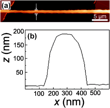 | ||
| Fig. 2 (a) AFM topography image of a single MEH-PPV nanofiber between Au electrodes. L = 15 μm. W = 320 nm. (b) Height profile of the fiber along the line marked by the arrows in (a). | ||
Electrical performances of single nanofiber field-effect transistors
Fig. 3a presents the current–voltage characteristics of a single nanofiber transistor with a fiber diameter of 500 nm (W) and a channel length (L) of 20 μm on a 100 nm-thick dielectric, for gate voltages (VGS) decreasing from 0 to −40 V. The drain current (IDS) dependence on the drain voltage (VDS) highlights a p-type behavior of the FET, working in accumulation mode. Fig. 3b displays the transfer characteristics, IDS(VGS), at a drain voltage of −50 V, together with the curve, |IDS|1/2 (VGS). This evidences a threshold voltage (VTH) of about −22 V by the slope of |IDS|1/2 in the saturation region [−VDS > −(VGS − VTH)]. While most of the here-fabricated devices exhibit such a negative value for VTH, which confirms their operation in accumulation mode, a few transistors show VTH > 0. This indicates accumulated holes possibly existing in the conduction channel even before a negative VGS is applied, probably due to impurities induced in the nanofibers during in air fabrication process.7 A mean saturation mobility (μ) value of 10−3 cm2/Vs, with a maximum of 5 × 10⁻³ cm2/Vs, is estimated by: , where Ci is the gate dielectric capacitance per unit area, evaluated as 32 nF cm−2 for the thermally-grown SiO2. The μ value is obtained by averaging the values measured in 40 devices, and by measuring the geometrical features (fiber diameter and channel length) of each device by SEM as in Fig. 1c. In the investigated samples, we could not appreciate a significant variation of the measured mobility depending on the fiber diameter. The conductivity of a single MEH-PPV nanofiber is up to 4.0 × 10⁻⁴ S cm−1 for VGS above threshold (−60 V). The Ion/Ioff switching ratios, i.e. the ratios between the maximum (“on”) and the minimum (“off”) IDS values measured in the transfer characteristics are calculated to be around 100, with a maximum as high as 780, which is comparable to values for electrospun P3HT nanofiber transistors (Ion/Ioff up to 103).4 Finally, the transconductance, gm = ∂IDS/∂VGS|VDS, is up to 0.26 nS for VDS = −50 V.
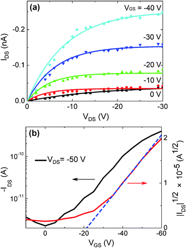 | ||
| Fig. 3 Output (a) and transfer (b) characteristics of a single MEH-PPV fiber FET, with 100 nm-thick SiO2 (L = 20 μm, W = 500 nm). (a) IDSvs. VDS curves for VGS = 0 V (squares), −10 V (circles), −20 V (upward triangles), −30 V (downward triangles), and −40 V (diamonds). Superimposed curves are best fits by FET characteristics. (b) IDS (left vertical scale) and |IDS|1/2 (right scale) vs. VGS for VDS = −50 V. The dashed curve is a linear fit to data in the saturation region (VGS > −35 V). | ||
Single fiber transistors on thicker SiO2 dielectric layers generally show mobilities reduced by a factor of four, and Ion/Ioff two times lower. As reference, we also fabricate MEH-PPV thin-film transistors by spin-coating the active polymer from chloroform solutions on 100 nm-thick dielectric layers. The hole mobility measured in these devices is found to be of 5 × 10⁻⁴ cm2 V−1 s−1, in agreement with previously reported data15 and one order of magnitude lower than the maximum values measured in nanofiber FETs with SiO2 of the same thickness.
Molecular alignment in ES nanofibers
The mobility in the nanofibers can be rationalized by considering a partial alignment of the polymer molecules. A preferential orientation would result indeed in an improved, ultimately quasi-1D conduction. This class of effects is largely studied for more ordered systems such as self-assembling π-stacking organic semiconductors.16 The intense electric fields involved in ES, related to both the anode-cathode bias and local electric charges on the collector electrodes, can in fact preferentially orient the polymer backbones, as investigated by infrared absorption and Raman spectroscopy.17 On the other hand, similarly to other conjugated polymer systems, fibers may exhibit inhomogeneities along their length, a feature which has been described by transport bridges supporting tunneling currents between adjacent domains of higher conductivity.18We carry out FTIR measurements on our fibers aligned into arrays (Fig. 4a), exploiting light polarized parallel and orthogonal with respect to the preferential direction in the array. FTIR spectra collected from MEH-PPV thin film do not evidence any polarization-dependence (data not shown). In fiber arrays, the peaks associated to vibrations prevalently directed along the molecular chain axis, such as the C–C ring stretch (1599 cm−1) and the vinylene C–H stretch (3020 cm−1),19 exhibit instead stronger intensities for light polarized parallel to fibers (solid line in Fig. 4a) with respect to excitation with orthogonally polarized light (dashed line). These results highlight a preferential molecular orientation along the fiber.
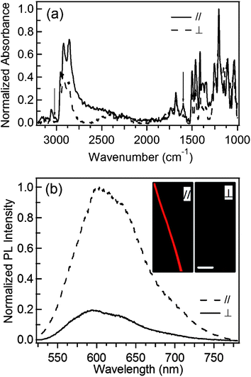 | ||
| Fig. 4 (a) FTIR spectra of MEH-PPV fiber arrays with excitation light polarized parallel (solid line) and orthogonal (dashed line) to fibers. The arrows indicate the modes at 1599 and 3020 cm−1. (b) Polarized PL spectroscopy of single MEH-PPV nanofiber. PL//(dashed line) and PL⊥ (continuous line). Insets: Corresponding fluorescence micrographs. Marker = 20 μm. | ||
Furthermore, to probe the supramolecular organization, polarized PL spectroscopy is carried out on single fibers, clearly showing that the signal collected through an optical polarizer with the polarization axis parallel (PL//) to the fiber is more intense than that collected with orthogonal polarization axis (PL⊥) (Fig. 4b). The resulting polarization ratio, χPL = PL///PL⊥ is up to (5.5 ± 0.5) for MEH-PPV fibers, indicating that the prevalent orientation of the emitting transition dipoles is parallel to fiber axis. We find similar results in fibers made by different PPV and polyfluorene-based polymers.20
PL quenching modulated by gate voltages
Another important feature stands in the possibility of tuning the emission characteristics by means of the applied bias. We study the PL properties of single MEH-PPV nanofibers lying on the operating transistors and excited by external blue light, thus using the FETs in the so-called luministor mode.21Fig. 5 shows a bright-field and a fluorescence micrograph of a single fiber device (with W = 700 nm and L = 30 μm), evidencing some luminescence scattering from fiber bulk inhomogeneities or surface defects, as observed in other light-emitting nanofiber materials.10 The PL spectrum from the nanofiber presents S1–S0 transitions with a 0–0 vibronic replica slightly more intense than the 0-1, i.e. with a relative decrease of the high-energy spectral component (λ < 600 nm) with respect to MEH-PPV films in FET geometry.10 Different vibronic structures, indicative of a relative reduction of interchain species formation, are observed in MEH-PPV fibers electrospun by tetrahydrofuran,20 but are not found to be associated with measurable mobilities and field effects when embedded in transistor devices.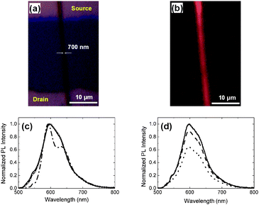 | ||
| Fig. 5 Bright field (a) and fluorescence (b) micrographs of a single light-emitting fiber FET (L = 30 μm, W = 700 nm) with VDS = VGS = 0 V. (c) Normalised PL spectra of thin film (dash–dotted line, peak wavelength, λmax = 592 nm, linewidth = 80 nm) and nanofiber embedded in a FET device with VDS = 0 V, and with VGS = 0 V (continuous line, λmax = 597 nm, linewidth = 81 nm) or −40 V (circles, λmax = 598 nm, linewidth = 81 nm). (d) Nanofiber PL spectra for VGS = 0 V (continuous line), −20 V (dashed line), and −40 V (dotted line). | ||
The PL spectral shape does not exhibit significant spectral variations upon changing the gate voltage (Fig. 5c). Instead, the PL intensity is quenched by a factor of 1.5 upon varying the gate voltage from 0 to −40 V, with VDS = 0 V (Fig. 5d), which corresponds to applied electric fields of the order of MV cm−1. This can be explained taking into account that, upon applying a negative bias to the gate, positive charges are induced in the layer of the fiber closer to the SiO2 surface. The PL is then effectively quenched because of nonradiative decay of singlet excitons by charge carriers into the polymer.21 Such PL quenching has been first analysed by modeling the 1D migration of photogenerated excitons to polarons/bipolarons annihilation centers, induced along the molecular chains by electrochemical doping in films of conducting polymers.22 At low (bi)polaron concentrations, the exciton diffusion towards PL quenching centers in polymer thin-film lumistors is instead considered to be mainly an interchain, three-dimensional mechanism,21 related to the accumulation of charges by the device capacitance. Other mechanisms may instead involve the field-induced dissociations of emitting species, as observed by sandwiching ladder-type poly(paraphenylene) in light-emitting diodes.23 A more comprehensive investigation of the observed PL quenching in our devices would require the characterization of the radiative and non-radiative decay channels of photo-excitation, by absolute quantum yield measurements and time-resolved spectroscopy on the single fiber. These experiments are currently in progress in our laboratories.
Conclusions
In summary, we realize single fiber FETs based on a prototype light-emitting polymer, measuring mobility values of the order of 10−3 cm2 V−1 s−1, and maximum Ion/Ioff values up to 780. The nanofibers PL can be electrically modulated. This study opens the way for their future integration in nano-scale optoelectronic devices such as flexible switches and light-emitting transistors. A main advantage of fully light-emitting polymer nanofibers, with respect to other conjugated polymers usually employed in transistors, such as the P3HT, relies on the possible future exploitation in optoelectronic circuits thanks to the well-known electroluminescence properties of PPV derivatives.24 Different device structures, using asymmetric Cr/Au and Al electrodes25 would be preferable for injecting efficiently holes and electrons in the active layer, thus leading to electroluminescence. In addition, the achievable performances can be widely tunable and enhanced by employing composite nanofibers incorporating inorganic nanocrystals within conjugated polymers.26Acknowledgements
We acknowledge the support from the FIRB RBIP06SH3W. This work is also performed in the framework of the FIRB RBFR08DJZI “Futuro in Ricerca”.Notes and references
- Y. Xia, P. Yang, Y. Sun, Y. Wu, B. Mayers, B. Gates, Y. Yin, F. Kim and H. Yan, Adv. Mater., 2003, 15, 353 CrossRef CAS.
- J. Xiang, W. Lu, Y. Hu, Y. Wu, H. Yan and C. M. Lieber, Nature, 2006, 441, 489 CrossRef CAS.
- A. Javey, J. Guo, Q. Wang, M. Lundstrom and H. Dai, Nature, 2003, 424, 654 CrossRef CAS.
- A. Babel, D. Li, Y. Xia and S. A. Jenekhe, Macromolecules, 2005, 38, 4705 CrossRef CAS; H. Liu, C. H. Reccius and H. G. Craighead, Appl. Phys. Lett., 2005, 87, 253106 CrossRef; S. Lee, G. D. Moon and U. Jeong, J. Mater. Chem., 2009, 19, 743 RSC; R. Gonzalez and N. J. Pinto, Synth. Met., 2005, 151, 275 CrossRef CAS.
- M. Hamedi, R. Forchheimer and O. Inganäs, Nat. Mater., 2007, 6, 357–362 CrossRef CAS; S. Virji, J. Huang, R. B. Kaner and B. H. Weiller, Nano Lett., 2004, 4, 491 CrossRef CAS.
- M. Steinhart, J. H. Wendorff, A. Greiner, R. B. Wehrspohn, K. Nielsch, J. Schilling, J. Choi and U. Gösele, Science, 2002, 296, 1997 CrossRef CAS.
- J. Liu, E. Sheina, T. Kowalewski and R. D. McCullough, Angew. Chem., Int. Ed., 2002, 41, 329 CrossRef CAS; F. Quochi, M. Saba, F. Cordella, A. Gocalinska, R. Corpino, M. Marceddu, A. Anedda, A. Andreev, H. Sitter, N. S. Sariciftci, A. Mura and G. Bongiovanni, Adv. Mater., 2008, 20, 3017 CrossRef CAS.
- D. Pisignano, G. Maruccio, E. Mele, L. Persano, F. Di Benedetto and R. Cingolani, Appl. Phys. Lett., 2005, 87, 123109 CrossRef; C. De Marco, E. Mele, A. Camposeo, R. Stabile, R. Cingolani and D. Pisignano, Adv. Mater., 2008, 20, 4158 CAS.
- D. H. Reneker and I. Chun, Nanotechnology, 1996, 7, 216 CrossRef CAS.
- S. Madhugiri, A. Dalton, J. Gutierrez, J. P. Ferraris and K. J. Balkus, J. Am. Chem. Soc., 2003, 125, 14531 CrossRef CAS; F. Di Benedetto, A. Camposeo, S. Pagliara, E. Mele, L. Persano, R. Stabile, R. Cingolani and D. Pisignano, Nat. Nanotechnol., 2008, 3, 614 CrossRef CAS.
- T. Sakanoue, E. Fujiwara, R. Yamada and H. Tada, Appl. Phys. Lett., 2004, 84, 3037 CrossRef CAS; F. Todescato, R. Capelli, F. Dinelli, M. Murgia, N. Camaioni, M. Yang, R. Bozio and M. Muccini, J. Phys. Chem. B, 2008, 112, 10130 CrossRef CAS.
- A. G. MacDiarmid, W. E. Jones Jr, I. D. Norris, J. Gao, A. T. JohnsonJr., N. J. Pinto, J. Hone, B. Han, F. K. Ko, H. Okuzaki and M. Llaguno, Synth. Met., 2001, 119, 27 CrossRef CAS; M. Wei, J. Lee, B. Kang and J. Mead, Macromol. Rapid Commun., 2005, 26, 1127 CrossRef CAS; S. Pagliara, A. Camposeo, A. Polini, R. Cingolani and D. Pisignano, Lab Chip, 2009, 9, 2851 RSC.
- A. Camposeo, F. Di Benedetto, R. Stabile, R. Cingolani and D. Pisignano, Appl. Phys. Lett., 2007, 90, 143115 CrossRef; F. Di Benedetto, E. Mele, A. Camposeo, A. Athanassiou, R. Cingolani and D. Pisignano, Adv. Mater., 2008, 20, 314 CrossRef CAS; A. Camposeo, F. Di Benedetto, R. Stabile, A. A. R. Neves, R. Cingolani and D. Pisignano, Small, 2009, 5, 562 CrossRef CAS.
- S. Grecu, M. Roggenbuck, A. Opitz and W. Brütting, Org. Electron., 2006, 7, 276 CrossRef CAS; J. B. Koo, S. H. Kim, J. H. Lee, C. H. Ku, S. C. Lim and T. Zyung, Synth. Met., 2006, 156, 99 CrossRef CAS.
- K. L. Tzeng, H. F. Meng, M. F. Tzeng, Y. S. Chen, C. H. Liu, S. F. Horng, Y. Z. Yang, S. M. Chang, C. S. Hsu and C. C. Chi, Appl. Phys. Lett., 2004, 84, 619 CrossRef CAS.
- J. Cornil, D. Beljonne, J.-P. Calbert and J.-L. Brédas, Adv. Mater., 2001, 13, 1053–1067 CrossRef CAS; M. D. Curtis, J. Cao and J. W. Kampf, J. Am. Chem. Soc., 2004, 126, 4318 CrossRef CAS.
- M. V. Kakade, S. Givens, K. Gardner, K. H. Lee, D. B. Chase and J. F. Rabolt, J. Am. Chem. Soc., 2007, 129, 2777 CrossRef CAS; A. Bianco, G. Iardino, A. Manuelli, C. Bertarelli and G. Zerbi, ChemPhysChem, 2007, 8, 510 CrossRef CAS; L. M. Bellan and H. G. Craighead, Polymer, 2008, 49, 3125 CrossRef CAS.
- N. A. Zimbovskaya, A. T. Johnson and N. J. Pinto, Phys. Rev. E, 2005, 72, 024213.
- D. D. C. Bradley, R. H. Friend, H. Lindenberger and S. Roth, Polymer, 1986, 27, 1709 CrossRef CAS.
- S. Pagliara, A. Camposeo, R. Cingolani and D. Pisignano, Appl. Phys. Lett., 2009, 95, 263301 CrossRef.
- P. Dyreklev, O. Inganäs, J. Paloheimo and H. Stubb, J. Appl. Phys., 1992, 71, 2816 CrossRef CAS.
- K. Kaneto, S. Hayahi and K. Yoshino, J. Phys. Soc. Jpn., 1988, 57, 1119 CrossRef CAS.
- S. Tasch, G. Kranzelbinder, G. Leising and U. Scherf, Phys. Rev. B: Condens. Matter, 1997, 55, 5079 CrossRef CAS.
- R. H. Friend, R. W. Gymer, A. B. Holmes, J. H. Burroughes, R. N. Marks, C. Taliani, D. D. C. Bradley, D. A. Dos Santos, J. L. Brédas, M. Lögdlund and W. R. Salaneck, Nature, 1999, 397, 121 CrossRef CAS; A. C. Grimsdale, K. L. Chan, R. E. Martin, P. G. Jokisz and A. B. Holmes, Chem. Rev., 2009, 109, 897 CrossRef CAS.
- T. Sakanoue, E. Fujiwara, R. Yamada and H. Tada, Chem. Lett., 2005, 34, 494 CrossRef CAS.
- A. A. R. Neves, A. Camposeo, R. Cingolani and D. Pisignano, Adv. Funct. Mater., 2008, 18, 751 CrossRef CAS; L. Persano, S. Molle, S. Girardo, A. A. R. Neves, A. Camposeo, R. Stabile, R. Cingolani and D. Pisignano, Adv. Funct. Mater., 2008, 18, 2692 CrossRef CAS.
| This journal is © The Royal Society of Chemistry 2010 |