Growth of horizontally aligned single-walled carbon nanotubes on anisotropically etched silicon substrate†
Carlo M.
Orofeo
a,
Hiroki
Ago
*abc,
Tatsuya
Ikuta
d,
Koji
Takahasi
d and
Masaharu
Tsuji
ab
aGraduate School of Engineering Sciences, Kyushu University, Fukuoka, 816-8580, Japan
bInstitute for Materials Chemistry and Engineering, Kyushu University, Fukuoka, 816-8580, Japan. E-mail: ago@cm.kyushu-u.ac.jp
cPRESTO, Japan Science and Technology Agency (JST), Kawaguchi, Saitama 332-0012, Japan
dGraduate School of Engineering, Kyushu University, Fukuoka, 819-0395, Japan
First published on 25th June 2010
Abstract
Directional controllability of single-walled carbon nanotubes (SWNTs) is an important issue for future nanoelectronics applications. For direct integration of carbon nanotubes with modern electronics, aligned growth of carbon nanotubes on SiO2/Si is desirable. We developed a new method to horizontally align SWNTs directly on SiO2/Si substrate by creating trenches on Si(100) through anisotropic etching followed by thermal oxidation. The V-shaped trenches highly improved the alignment of SWNTs and the degree of alignment is comparable to the step-templated alignment of carbon nanotubes on crystals. The trenches also improved the density of aligned nanotubes due to the combination of “trench-guided” and gas-flow guided alignment. Our new insights on carbon nanotube alignment on SiO2/Si will greatly contribute to future large-scale nanoelectronic applications.
Introduction
Single-walled carbon nanotubes (SWNTs) have been considered as one of the promising materials for future technologies due to their exceptional mechanical and electrical properties.1 For applications in nanoelectronics, the capability to control both the position and direction of SWNTs is of utmost importance for the integration of SWNTs to the current silicon-based electronics. This is because silicon-based electronics are configured in a highly ordered geometry. Also, the nanoscale diameter of a SWNT is ideal for further integration or miniaturization of devices. Several studies have been made to characterize the device performance of a network comprising random and overlapping nanotubes by comparing with an array of horizontally-aligned nanotubes.2–4 These studies suggested that tube–tube contacts within the nanotube array greatly affect the overall device performance. For instance, it was recently reported that the junctions of the intertwined SWNT increase the resistance and that the junctions control the overall network performance.4Moreover, direct growth of aligned and isolated SWNTs on silicon substrate with an oxide layer (SiO2/Si) using conventional chemical vapor deposition (CVD) methods is desirable for direct integration into the current electronic devices. However, due to the amorphous nature of SiO2, SWNTs grown on SiO2/Si are randomly oriented and overlap each other,5,6 unlike in crystal substrates where horizontal alignment is self-assembled.7–14 This led to several researches specifically aimed on the alignment of SWNTs on SiO2/Si.15–25
Successful alignment of SWNTs on SiO2/Si was achieved by either controlling the CVD condition or modification of the substrate. A widely used example in the former case is gas-flow directed alignment.16–20 It was suggested in this method that the SWNT aligns along a laminar flow of gas used during CVD growth. This method assigns the “kite-flying” mechanism as responsible for the alignment.17 The mechanism suggests that during growth, the catalyst is located at the SWNT tip while floating on top of the substrate (tip-growth) thereby avoiding contact with the substrate and thus, consequently providing an argument to the long nature (up to several centimetres) of the SWNTs produced. However, the argument of producing a long SWNT with the catalyst remaining on the surface (base-growth) was also being raised by other group.20 Electric field-induced alignment during CVD growth was also reported,15 but the degree of alignment is insufficient and it requires electrical wiring that works at high CVD temperature.
Recently, we have demonstrated alignment of SWNT based on the second approach. Our method requires modification of the SiO2/Si substrate to create trenches and guide the growth of SWNTs.24 We have proposed that SWNTs were caught at the edges of the reactive ion etched (RIE) square-shaped trenches, thus aligning the nanotubes along the edge. However, SWNTs escaped due to the inconsistent shape of the trench giving a lesser degree of alignment compared to the gas-flow directed alignment.24,25 Our previous results suggested that trench structure is essential for improving the degree of SWNT alignment.
In this paper, we improved the trench structure by using anisotropic etching of Si wafers to produce V-shaped trenches, which uses the different etching rates of Si{111} and Si{100} surfaces against potassium hydroxide (KOH) etching solution. The trench shape is expected to be more defined in terms of structure than the previous RIE etched trenches. We have created V-shaped trenches with depths between 150 nm and 300 nm, in which gas flow on trenches appeared to affect the growth and alignment of SWNTs. Anisotropic etching of Si substrates is widely used for microelectromechanical system (MEMS), but relatively large-scale structures with scale over 1 μm are fabricated.26 Here, we developed a new method to create a several 100 nm-scale patterns for the manipulation of SWNT growth.
By combining both the proposed alignment mechanisms, this paper presents a new insight of aligning SWNTs with higher density and higher degree of alignment compared to the previously reported results.16–20,24,25 Moreover, we will show that both gas-flow assisted and “trench-assisted” alignment contributed to the improvement of density and degree of alignment. Lastly, parameters like temperature, gas flow rate, gas flow direction, and trench widths were varied in order to investigate scalability. The possible mechanism for alignment will be discussed based on these data.
Experimental
Anisotropic etching of Si(100)
A schematic diagram of the process is shown in Scheme 1. Wafers of Si(100) with a 300 nm surface oxide layer were purchased from SUMCO Corp. For this work, SiO2 was used as a mask, as anisotropic etching requires a hard mask. The 300-nm oxide layer was etched to ∼100 nm by soaking the substrate in buffered hydrofluoric acid (BHF) solution at room temperature in order to make the oxide thin enough for better control during RIE. Spin coating of positive electron beam (EB) resist (ZEP520A, Zeon Corp.) and carefully aligning the substrate's pattern parallel or perpendicular to the <110> direction prior to EB lithography created a mask pattern (Scheme 1a). The position of the mask pattern is critical to the formation of V-shaped trenches since the {111} planes intersect at a specific crystallographic direction that gives a square-based pyramid pit shape on Si(100).26,27 The different SiO2 line pattern openings of 200–500 nm (with constant spacing of 500 nm) and up to 1 mm in length, exposed after developing (ZED-N50) and rinsing (ZMD-B), were then subjected to RIE (SAMCO 10iP) using CF4 gas to remove the SiO2 and expose the silicon surface which was not covered with the EB resist (Scheme 1b). | ||
| Scheme 1 Schematic diagram showing the method to grow horizontally aligned SWNTs on patterned silicon. To create the pattern, anisotropic etching of Si(100) was done by aligning an SiO2 mask parallel or perpendicular to Si<110> prior to anisotropic etching (see text for details). The mask was defined by EB lithography. | ||
Orientation-dependent etching was done by soaking the SiO2-masked silicon into KOH solution of DI water (30 wt%) at 80 °C for 1 min. It is known that (100)-oriented surfaces etch 100 times faster than (111)-oriented surfaces on KOH.26,27 With proper mask orientation, a precise V-shaped groove can be formed with Si{111} surfaces making an angle of 54.7° with respect to Si(100). After etching, the SiO2 mask was completely removed by soaking in BHF for 3 min (Scheme 1d). The etched silicon was annealed under Ar gas at 900 °C for 3 h (100 sccm), prior to thermal oxide growth, to sharpen the V-shaped trenches. Then, the substrate surface was oxidized by heating the substrate at 900 °C while flowing oxygen (200 sccm) bubbled through heated (95 °C) DI water (Scheme 1e). The thickness of SiO2 can be controlled by exposure time which in our case is equivalent to ∼200 nm.
CVD growth of SWNTs on trenched silicon
The stripe pattern of Fe catalyst was made by radio frequency (RF) magnetron sputtering (Shibaura Mechatronics Corp., CFS-4ES) on a 10-μm photoresist with openings spaced at 100 μm that was previously patterned and positioned perpendicular to the substrate's trenches. The thickness of the catalyst was controlled to <1.0 nm, which gave the highest nanotube yield. After lift-off with acetone, the substrate was subjected to alcohol CVD (Scheme 1f). After reaching 900 °C in an Ar flow, a 80 sccm flow of H2 was introduced for 5 min to reduce the Fe catalyst, followed by nanotube growth with a flow of H2 (80 sccm) and Ar (300 sccm) bubbled through ethyl alcohol (EtOH) that was chilled at 0 °C. Geometrical structures of nanotubes and trenches were observed with a scanning electron microscope (SEM, HITACHI S-4800), a scanning transmission electron microscope (STEM, HITACHI HD 2300), and a transmission electron microscope (TEM, HITACHI H-9500). Atomic force microscopy (AFM, Veeco Nanoscope IIIa) was used to profile the trenches and Raman maps were generated using micro-Raman spectrometer (JASCO NRS-2100) equipped with an Ar ion laser (514.5 nm) directed onto the substrate at a ∼1 μm spot size.Results and discussion
Fig. 1a shows a STEM image of our trench profile created on Si substrate. Two different crystalline planes can be seen at the Si interface; the original Si(100) plane and the Si{111} plane that appeared after anisotropic etching. The SiO2 layer, which was formed after anisotropic Si etching, fully covered the Si surface. It is noted that the original Si surface has a relatively smooth V-groove but the SiO2 layer gave sharp bottom edges. Shown in Fig. 1b is a close up TEM image of the sidewall of the V-shaped groove. This cross-sectional view of Si{111} surface was seen from one of the {110} planes. The Si substrate showed a well-defined fcc lattice structure, while SiO2 was completely amorphous. The inset image is the diffraction pattern of the Si substrate. | ||
| Fig. 1 STEM (a) and TEM (b) images of the trenches created on silicon surface. Both images were viewed from the Si{110} direction. The inset of (b) is a diffraction pattern image obtained from the Si matrix. | ||
Fig. 2a shows the SEM image of the aligned nanotubes on the trenched silicon grown from EtOH as carbon source. The carbon nanotubes were grown from the upper area where the patterned Fe-catalyst is located. It can be seen that the grown nanotubes are straight and distinct from each other. The nanotubes appeared as thick white lines due to the charging effect. Most of the nanotubes are ∼100 μm in length; relatively shorter than those from the gas-flow-directed growth. A large scale image of the substrate is shown in Fig. 2b, which clearly shows the scalability of the method. The degree of alignment of the grown nanotubes is comparable to the preliminary works of aligned carbon nanotubes grown on stepped-crystal substrates.8,11 We shall be discussing later that this improvement in alignment was influenced by the presence of trenches.
 | ||
| Fig. 2 (a) SEM image of aligned nanotubes on trenched silicon. (b) Large scale image of the aligned nanotube arrays. The white horizontal stripes are the catalyst patterns. (c) High magnification SEM image of one of the aligned nanotubes on the trench. Indicated are the nanotubes and the trenches. Top refers to the top of the trench and bottom refers to the bottom of the trench. In this image, the nanotube follows the bottom of the trench. (d) G-band intensity map of the aligned nanotube. A long nanotube with total length of > ∼100 μm is indicated by an arrow. (e) Raman spectrum on the aligned SWNT shown in (c). | ||
A high resolution SEM image of the confined nanotubes is seen in Fig. 2c. The trench structure is indicated and clearly dictates the alignment direction of the carbon nanotubes (indicated in the arrows). From our observations, there is no clear and constant alignment position of carbon nanotubes within the trenches, but they generally give the directionality of the alignment (for example, the nanotube shown in Fig. 2c aligned along the bottom of the V-trench). Further discussions on the alignment will be presented later. Fig. 2d shows the spatial intensity of a G-band (∼1580 cm−1) measured from one of the aligned nanotubes, which confirms that the white line represents a carbon nanotube. A long nanotube is indicted by the arrow. A sample Raman spectrum on one of the aligned nanotubes is presented in Fig. 2e. A clear G-band and radial breathing mode (RBM) were observed. We did not see a significant D-band peak, which should appear at 1350 cm−1, indicating that the as-grown SWNT is of high quality. From the observed RBM, ω of ∼175 cm−1, the diameter is estimated to be d = 1.4 nm using the expression d = 248/ω (in nm), an indication that the grown nanotubes are single-walled. In the area close to the catalyst pattern, short carbon nanotubes were found which is consistent with studies involving growth of carbon nanotubes on an SiO2/Si substrate.16,17,22 Closer investigation of the SEM image in Fig. 2a reveals that some short nanotubes align along the direction of the trenches. This leads us to investigate the nature of alignment of the nanotubes for our process; i.e. if alignment is “trench-assisted” or gas-flow induced. Fig. 3a contrasts the alignment of SWNTs on the boundary of the patterned (right side of the white border) and plain substrate (left side of the white border). Obvious differences in terms of alignment are seen, with random nanotubes growing on the plain substrate. It is clear that the trenches greatly improved the degree of alignment.
 | ||
| Fig. 3 SEM images of aligned SWNTs on trenched Si substrates. (a) Comparison of the plain and trenched silicon substrate in terms of the alignment of SWNTs. (b–d) Influence of the rotation angle of the trenched silicon against the gas flow at different angles. | ||
Previous results on gas-flow directed alignment suggests that once a “kite-flying” SWNT drops onto a plain SiO2 surface, the nanotube grows in random direction and soon terminates its growth.19 This observation is also possible if the growth mode is base-growth; that is the catalyst stays on the surface and the nanotubes slides. Reina et al. suggested that there is a certain critical length needed for gas-flow induced alignment to occur.20 For this type of growth mechanism, we speculate that the presence of trenches prevents random sliding but instead guides the nanotubes along the trenches. Thus near the catalyst pattern, relatively short lengths (<40 μm) of aligned SWNTs can be frequently found.
To further investigate the effect of trenches on the alignment, the trench pattern's direction was varied with respect to the gas flow direction by changing the sample orientation. This method allows the investigation of the contribution of the trenches and gas flow to the alignment of carbon nanotubes. Fig. 3b–3d shows the carbon nanotubes' alignment dependence on the gas flow direction with respect to the trenches. Interestingly, there was still nanotube alignment even if the substrate was rotated at 30°. In fact, not much difference was seen from the slightly rotated substrate (15°, Fig. 3b). At 30° rotation, similar alignment along the trenches was seen as in the un-rotated (Fig. 3a). However, some nanotubes were bent along the direction of the gas flow (indicated by yellow arrows), while some grow along the direction of the trenches unaffected by the gas flow. For the latter case, we argue that the alignment was trench-guided. At 90° rotation (Fig. 3d), typical gas-flow aligned SWNTs were predominant. However, short nanotubes which are aligned along the trench pattern were also present near the catalyst pattern. It is worth noting that the density of gas-flow aligned carbon nanotubes in Fig. 3d is not as high as the un-rotated or slightly rotated substrates. Therefore, the aligned nanotubes in Fig. 3b–3c cannot all contribute to the gas flow. We believe that the alignment of the nanotubes was realized by a combination of gas-flow induced and trench-induced alignment.
Furthermore, we note that the aligned nanotubes grew in both directions from the catalyst line. Aligned carbon nanotubes that grow opposite the gas flow must be trench-induced, because the gas-flow induced the nanotubes to grow downstream of the CVD reactor. Plotted in Fig. 4a is the distribution of length of nanotubes on one of a 10-mm long catalyst line of the substrate from Fig. 2b. This count per unit length will be the basis of comparison from other studies. As a comparison, our total density for nanotubes with length ∼100 μm at 67 nanotube/10 mm is roughly at least twice than the previously reported gas-flow directed results.16–20 The forward length refers to the length of the carbon nanotubes that were aligned in the direction of the gas flow and the backward length is the length of the nanotubes that were aligned against the gas flow. It can be seen that the forward length (red) has two different length distributions; broad, 10–90 μm, and sharp, >100 μm. Because the distance between the catalyst lines is 100 μm, the long tubes of >100 μm are counted as 110 μm. Therefore, it can be argued that most of the forward-grown nanotubes are grown via a “kite-flying” mechanism where it is expected to be longer. For the trenches to influence the alignment, the carbon nanotube must be sliding. The relatively smooth SiO2 surface as shown in Fig. 1a allows the nanotubes to slide along the surface. Thus, the short nature of carbon nanotubes in both the forward and reverse direction is expected as it must overcome the frictional forces brought about by the SWNT–substrate interaction (due to the not-so-atomically-flat substrate) during sliding.
 | ||
| Fig. 4 (a) Length distribution of the aligned SWNTs in Fig. 2b. Forward and backward refers to the direction of the growth of the nanotubes with respect to the gas flow direction. (b) Length distribution of the aligned SWNTs along the trenches in Fig. 3d (the number of SWNTs aligned parallel to the gas flow is not indicated in the histogram). Top and bottom refers to the direction of the nanotubes with respect to the location of the catalyst line (forward/backward is not used because the gas flow is normal to the trenches). The total length of the catalyst line by which the nanotubes were counted is 10 mm. | ||
The occurrence of both the sliding and “kite-flying” mode of alignment can be greatly contrasted by rotating the substrate by 90° prior to CVD growth as was shown in Fig. 3d. This allows us to distinguish the gas-flow induced and trench-guided alignment. The histogram shown in Fig. 4b is the number density of the nanotubes aligned along the trenches (trench-induced) of the substrate in Fig. 3d. The top and bottom indicates the position of the catalyst where the carbon nanotubes are originating (the number of gas-flow assisted alignments is not displayed). Most nanotubes were relatively short (10–20 μm) and are growing from both sides of the catalyst pattern. Obviously the SWNTs shown in Fig. 4b are trench-guided.
From the above results, we conclude that in order to attain highly dense and aligned nanotubes, it is necessary to keep the nanotubes sliding by an extended growth duration, assuming that the catalysts remain active. Growth timing studies were performed and the results are shown in Fig. 5. Growth timing studies can also show the differences of the two alignment modes presented here. Gas-flow aligned SWNTs are expected to be longer than the trenched-induced aligned SWNTs. Indeed in Fig. 5a–5c, we see long and short nanotubes. In Fig. 5a, long nanotubes are seen, although the growth duration was only 5 min. As the growth time increases, the number of relatively long nanotubes also increases. We believe that the aligned nanotubes shown in Fig. 5b and 5c are a combination of gas-flow induced and trench-induced alignment. The density of the long and aligned nanotubes increased with increased growth time. So, we speculate that the synergetic effect of gas-flow and trenched-induced alignment greatly enhanced the density of the aligned SWNTs.
 | ||
| Fig. 5 SEM images of the carbon nanotubes after different CVD growth times: (a) 5, (b) 30, and (c) 60 min. | ||
Here, we discuss the improved degree of alignment of SWNTs on our trenched silicon. As was previously shown, the gas-flow induced grown nanotubes can be aligned in the trenches even if the trench direction is slightly rotated from the gas flow direction. Two mechanisms were proposed for this. First, the presence of trenches modified the local gas flow and changes gas flow direction such that it is directed along the trenches. However, the creation of a desirable local gas flow is limited to certain degrees (∼30° rotation), as was presented previously. Different trench profiles were investigated to determine its effects on the alignment. Fig. 6a shows a trench profile of wider width (∼700 nm) that was half-etched. Inset in Fig. 6a is an AFM image of the trench profile. It resulted in a lesser degree of alignment compared to the V-shaped trench. This may be due to the different gas flow profiles of the half-etched and V-shaped trenches. Also, the absence of V-shaped edge may not assist the trench-induced alignment. It is noted that at different gas flow rates and EtOH/H2 ratio also resulted in poor to no alignment (see the Fig. S1 and S2 in the ESI†). These observations show the importance of the gas flow profile to the alignment of the nanotubes. Theoretical studies are needed to understand the gas flow effects on different trenches.
 | ||
| Fig. 6 (a) SEM image of the aligned carbon nanotube on a squared shaped trench with a wide trench and a half-etch. Inset is the AFM profile of the trench. (b) SEM image of an aligned nanotube on a substrate that was rotated 30°. Straight and bent portion of the nanotube can be seen. (c) SEM image of suspended nanotubes (indicated in the arrows) in a 2-μm long well. | ||
The other explanation for the improved degree of alignment is similar to the mechanism proposed for the formation of serpentine carbon nanotubes.28 Briefly, this two-step mechanism starts with the tip-growth of a suspended nanotube along the direction of the gas flow followed by an oscillatory fall process where the nanotube adsorbs onto the surface along the step. At a different gas flow direction with respect to the steps, different carbon nanotube geometries, including serpentine carbon nanotubes, can be formed.28 For stepped crystal substrates, the combined forces of surface adhesion from the substrate–carbon nanotube interaction and the aerodynamic drag caused by the gas-flow induced bending of carbon nanotubes. Similarly in our case, the alignment of nanotubes occurs at the time when the length of the grown nanotubes drops under its own weight during growth and aligns its length along the trench. However, there is a limitation to the misalignment of the trenches and gas flow direction for such a mechanism to occur. No bending of nanotubes was seen when the substrate was rotated at 90° with respect to the gas flow direction because, we think, that the distance between trenches is far enough that it cannot influence and induce alignment in the same manner as described previously;28 that is, the aerodynamic force from the gas is the only dominant force during alignment. Fig. 6b shows an SEM image of the substrate with trenches rotated at 30° with respect to the gas flow. Straight and aligned nanotubes aligned along the trench (shown in I), bend at Region II, and straightened again in Region III. Note that in Region II, the bent part was aligned with the gas flow direction which can be explained by the serpentine carbon nanotube formation mechanism. Another proof of the mechanism is the presence of suspended nanotubes on a 2 μm well-shaped barrier created between the catalyst patterns as shown in Fig. 6c. The suspension of the nanotubes on the well-shaped barrier clearly proves that nanotubes are grown by a kite-flying mechanism. It can also be observed that it realigns in another trench after crossing the well-shaped barrier, an observation on the influence of V-shaped trenches on the alignment.
Previous studies show that temperature plays an important role in the growth of gas-flow-aligned SWNT in alcohol CVD system.22,29 These studies also suggest that there is a balance between gas flow alignment and density. Gas-flow induced alignment favors high temperature but also favors formation of amorphous carbon and graphite, decreasing the density. This trade-off is interesting to see in our system, since the primary goal is to achieve aligned and dense nanotubes. Fig. 7a shows an SEM image of aligned carbon nanotubes grown at 850 °C. The same degree of alignment was seen but the density was lower compared to nanotubes grown at 900 °C, because the catalyst activity depends on CVD temperature. As the temperature is increased to 950 °C, we noticed that the trenches cannot influence the alignment. As shown in Fig. 7b the familiar gas-flow directed alignment was seen. It is also noted that at higher temperature, amorphous carbon sticking to carbon nanotubes can be observed, consistent with alcohol-CVD-grown nanotubes at higher temperatures.21 We take note that the trench profile is stable at the higher CVD temperature and no noticeable changes in the profile was seen (Figure S3 in the ESI†). This observation can have an implication on our proposed alignment theory. At higher temperature, gas flow alignment is favorable and disrupts or changes the gas profile such that the trenches cannot induce alignment.
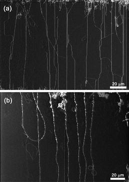 | ||
| Fig. 7 SEM images of the carbon nanotubes grown at different temperatures: (a) 850 °C (lower than normal) and (b) 950 °C (higher than normal). | ||
It has been accepted that gas-flow induced alignment is the major mechanism for aligning carbon nanotubes on an SiO2/Si substrate. Here, we present that carbon nanotubes can also be aligned with the aid of trenches. This “trench-induced” alignment is due to the confinement of carbon nanotubes within the trenches as it slides during growth. Furthermore, the presence of an appropriate trench structure is necessary to further improve the density and degree of alignment of nanotubes regardless of the alignment mechanism.
Conclusions
We have succeeded in aligning SWNTs directly grown on SiO2/Si substrate with artificial trenches. The V-shaped trench was created by anisotropically etching Si(100) prior to growing SWNTs. Our grown nanotubes have a higher degree of alignment than the normal gas-flow induced aligned carbon nanotubes. Moreover, the degree of alignment was improved by the presence of trenches. The combination of gas-flow induced and trench-induced alignment enhanced the total SWNT density. We have proposed that the trench profile and temperature can affect the degree of alignment. It is expected that our method can greatly contribute to the integration of carbon nanotubes in nanoelectronics where high density is desirable and high controllability is a requirement.Acknowledgements
This work was supported by the Grant-in-Aid for Scientific Research from MEXT and PRESTO-JST. CMO acknowledges the support from Global COE project (Novel Carbon Resource Sciences) for partially funding this research.References
- R. H. Baughman, A. A. Zakhidov and W. A. de Heer, Science, 2002, 297, 787 CrossRef CAS.
- C. Kocabas, N. Pimparkar, O. Yesilyurt, S. J. Kang, M. A. Alam and J. A. Rogers, Nano Lett., 2007, 7, 1195 CrossRef CAS.
- S. J. Kang, C. Kocabas, T. Ozel, M. Shim, N. Pimparkar, M. A. Alam, S. V. Rotkin and J. A. Rogers, Nat. Nanotechnol., 2007, 2, 230 CrossRef.
- P. N. Nirmalraj, P. E. Lyons, S. De, J. N. Coleman and J. J. Boland, Nano Lett., 2009, 9, 3890 CrossRef CAS.
- J. Kong, H. T. Soh, A. M. Cassell, C. F. Quate and H. Dai, Nature, 1998, 395, 878 CrossRef CAS.
- E. S. Snow, J. P. Navak, P. M. Campbell and D. Park, Appl. Phys. Lett., 2003, 82, 2145 CrossRef CAS.
- H. Ago, K. Nakamura, K. Ikeda, N. Uehara, N. Ishigami and M. Tsuji, Chem. Phys. Lett., 2005, 408, 433 CrossRef CAS.
- A. Ismach, L. Segev, E. Wachtel and E. Joselevich, Angew. Chem., Int. Ed., 2004, 43, 6140 CrossRef CAS.
- S. Han, X. Liu and C. J. Zhou, J. Am. Chem. Soc., 2005, 127, 5294 CrossRef CAS.
- C. Kocabas, S. H. Hur, A. Gaur, M. A. Meitl, M. Shim and J. A. Rogers, Small, 2005, 1, 1110 CrossRef CAS.
- H. Ago, K. Imamoto, N. Ishigami, R. Ohdo, K. Ikeda and M. Tsuji, Appl. Phys. Lett., 2007, 90, 123112 CrossRef.
- L. Ding, D. Yuan and J. Liu, J. Am. Chem. Soc., 2008, 130, 5428 CrossRef CAS.
- C. Kocabas, S. Kang, T. Ozel, M. Shim and J. A. Rogers, J. Phys. Chem. C, 2007, 111, 17879 CrossRef CAS.
- N. Ishigami, H. Ago, K. Imamoto, M. Tsuji, K. Iakoubovskii and N. Minami, J. Am. Chem. Soc., 2008, 130, 9918 CrossRef CAS.
- A. Ural, Y. Li and H. Dai, Appl. Phys. Lett., 2002, 81, 3464 CrossRef CAS.
- S. Huang, X. Cai and J. Liu, J. Am. Chem. Soc., 2003, 125, 5636 CrossRef CAS.
- S. Huang, M. Woodson, R. Smalley and J. Liu, Nano Lett., 2004, 4, 1025 CrossRef CAS.
- Z. Yu, S. Li and P. J. Burke, Chem. Mater., 2004, 16, 3414 CrossRef CAS.
- L. X. Zheng, M. J. O'Connell, S. K. Doorn, X. Z. Liao, Y. H. Zhao, E. A. Akhadov, M. A. Hoffbauer, B. J. Roop, Q. X. Jia and R. C. Dye, et al, Nat. Mater., 2004, 3, 673 CrossRef CAS.
- A. Reina, M. Hofmann, D. Zhu and J. Kong, J. Phys. Chem. C, 2007, 111, 7292 CrossRef CAS.
- Y. Qian, S. Huang, F. Gao, Q. Cai, L. Zhang and W. Hu, J. Phys. Chem. C, 2009, 113, 6983 CrossRef CAS.
- L. Zheng, B. C. Satishkumar, P. Gao and Q. Zhang, J. Phys. Chem. C, 2009, 113, 10896 CrossRef CAS.
- N. Yoshihara, H. Ago, K. Imamoto, M. Tsuji, T. Ikuta and K. Takahashi, J. Phys. Chem. C, 2009, 113, 8030 CrossRef CAS.
- C. M. Orofeo, H. Ago, N. Yoshihara and M. Tsuji, Appl. Phys. Lett., 2009, 94, 53113 CrossRef.
- T. Kamimura and K. Matsumoto, Appl. Phys. Express, 2009, 2, 15005 Search PubMed.
- K. Bean, IEEE Trans. Electron Devices, 1978, 25, 1185–1193 CrossRef.
- S. M. Sze, Semiconductor Devices: Physics and Technology in Lithography and Etching, John Wiley & Sons, 2nd edn, New York, 2001, pp 428–429 Search PubMed.
- N. Gelblinger, A. Ismach and E. Joselevich, Nat. Nanotechnol., 2008, 3, 195 CrossRef.
- B. Zhang, G. Hong, B. Peng, J. Zhang, W. Choi, J. M. Kim, J. Choi and Z. Liu, J. Phys. Chem. C, 2009, 113, 5341 CrossRef CAS.
Footnote |
| † Electronic supplementary information (ESI) available: SEM images of SWNTs grown under different CVD conditions. See DOI: 10.1039/c0nr00170h |
| This journal is © The Royal Society of Chemistry 2010 |