Ink-jetable patterning of metal-catalysts for regioselective growth of nanowires
David
Zopes
,
Robin
von Hagen
,
Ralf
Müller
,
Raquel
Fiz
and
Sanjay
Mathur
*
University of Cologne, Division of Inorganic and Materials Chemistry, Greinstrasse 6, D-50939, Köln, Germany. E-mail: sanjay.mathur@uni-koeln.de; Fax: (+49) 221 470 4899; Tel: (+49) 221 470 5627
First published on 4th August 2010
Abstract
Nanosized (20–30 nm) colloidal gold, silver and their alloys were obtained by reductive transformation of corresponding metal salts. Dispersions of metal nanoparticles (σ < 4%) in aqueous solutions were obtained by appropriate surface functionalization which led to inorganic inks with solid fraction ranging from 0.01–4%. Judicious choice of a polymer additive (polyethylene glycol or carboxymethyl cellulose) was found to be crucial to avoid the agglomeration of nanocrystals in the ink-jetted structures upon solvent evaporation. The versatility of the nanoparticle-based printing technology was demonstrated by fabrication of dot-matrices and circuitry patterns on different substrates. Characterization of printed structures showed a homogeneous topography (AFM) and uniform distribution of metallic nanoparticles (SEM/TEM) within the ink-jetted microdrops. The site-specific patterning on silicon (001) substrates with nanoparticle (mono)layers could also be achieved by printing the linker molecule, aminopropyltriethoxysilane, followed by selective attachment of gold nanoparticles. Positionally ordered and chemically bonded gold catalyst patterns were used for the chemical vapour deposition (CVD) of nanowires, which led to site-specific growth of nanowires via the vapour-liquid-solid (VLS) mechanism and unlike in the case of spin-coated metal colloids no significant lateral diffusion of metal nanoparticles was observed, in chemically anchored Au nanoparticles. Nanoparticle containing inks allow a user-defined dilution to vary the density of CVD grown nanowires, which was utilized to show the differences in catalytic activities of silver and gold catalysts in the VLS growth.
Introduction
Inkjet printing is a familiar method for printing texts and images using organic dyes or pigments and is integrated in modern professional and household routines.1 In the last few years it has found increasing application as a free-form fabrication technique for building diverse micro-structures on various substrates. A high positional accuracy of printing chemical ink together with cost-efficiency and high flexibility makes it an attractive approach towards hydro/solvo-dynamic structuring of nanocrystals on various substrates. Subjected to the targeted applications, the chemical compositions reach from polymers, aqueous salt or precursor solutions to different dispersions of nano-sized metal or metal oxide.1–4Examples of inkjet printing in the fabrication of functional microstructures include printed electronics,1 lubricants for micromechanical parts1 or defined polymer deposition for manufacturing multicoloured displays.2 The dispersions of inorganic colloids and organic dyes can be dispensed in a continuous or on-demand mode. However, the printing configurations3 in general consists of a dispensing-head connected to an ink-reservoir that is filled and maintained with the ink through pressure difference. The core of the dispensing-head is a glass capillary surrounded by a piezo actuator. A voltage pulse contracts the piezo actuator thereby creating a pressure wave which is amplified to dispense a small column of the liquid.4 The strength of the pulse, the used solvent and the diameter of the nozzle diversifies thereby drop size and printing speed.5
In this study, colloidal dispersions of Ag, Au and Ag–Au alloy nanoparticles were used as inorganic inks to fabricate positionally defined microstructures for catalytic applications such as decomposition of metal–organic precursors on metal nanocrystals to impart preferential (anisotropic) growth of nanostructures. Noble and transition metal particles are extensively used as growth templates for synthesizing nanowires and nanotubes of different materials.6 However, their deposition is generally achieved by physical methods (e.g., sputtering of metallic targets, spin-coating of colloids), which leads to a random distribution of catalyst particles on the substrate. In this context, inkjet printing of catalysts allows fabrication of periodic arrays and site-specific deposition of functional nanostructures7,8 what plays an important role in controlled positional assembly for device applications. The recent developments include methods involving the chemical patterning, whereby a bi-functional linker molecule is immobilized on the substrate in the regions of interest by site-selective printing of the linker such as aminopropyltriethoxysilane (APTES), which binds the gold colloids on the surface by strong chemical interaction.9 Self assembled nanoparticle monolayers on silicon10,11 as well as inkjet printed self assembled alkanethiols12 on noble metal substrates are well-known. Herein a combination of inkjet printed self assembled monolayers on silicon was shown to obtain regioselective dense packed layers of gold colloids useful for a wide range of possible applications reaching from chemical sensing to novel electrical devices.13
Semiconducting materials in nanoscopic forms exhibit unique electronic, optical and transport properties which scale-up with the degree of dimensional confinement.14 SnO2 is a wide bandgap semiconductor (Eg = 3.6 eV) and therefore transparent in visible light making it a useful material for conductive electrodes and anti-reflective coatings. Furthermore SnO2-based materials are very suitable for gas sensing devices due to their high sensitivity towards reducing gases (such as carbon monoxide) which results from a strong influence of the adsorbed gases on the intrinsic conductivity of the material.15 This transduction (charge transfer) phenomenon is a function of surface-to-volume16 ratio that makes tin oxide nanostructures preferred candidates for gas sensors.
The synthesis for SnO2 nanowires by chemical vapour deposition (CVD) on gold catalysts follows the vapour–liquid–solid (VLS) mechanism, originally postulated by Wagner and Ellis for the growth of silicon whiskers,6 had been reported.17 At CVD growth temperatures (550–800 °C) the sputtered thin gold layer disintegrates, due to intrinsic stresses and differential thermal expansion coefficients, into particles in the range of 50–1000 nm, whereby the particle size is a function of film thickness and is governed by the surface tension in spherical clusters.17 This method however, offers limited control on the distribution of metal clusters; also the high polydispersity in obtained nanoparticles limits the control over the axial and radial dimensions in as-grown nanowires and whiskers. Furthermore, it is cumbersome to coat different types of metal on the same substrate (achievable through masking and etching procedures) and there is also a low-concentration-limit for the particles which can not be under-run. All these aspects restrict the practicality of the CVD method in the controlled and selective synthesis of SnO2 (or any other metal oxide) nanowires.
In this report, we describe deposition of metal catalysts on various substrates using nanoparticle dispersions as inks for inkjet printing with narrow size-dispersion and controllable particle concentration. Inkjet printing with nano-inks permitted a flexible and fast printing of different metal catalysts on a single substrate that enabled regio-selective growth of nanowires by CVD process. In addition, printing of aminopropyltriethoxysilane monolayer as primer allowed a chemical fixation and site-specific dense arrays of metal catalysts for CVD process. These new options substantially enhance the potential of CVD process and may have technological implications for the rapid and reproducible processing of CVD-grown nanostructures.
Experimental
The gold and silver nanoparticles were synthesized according to procedures reported in the literature.18,19 The silver–gold alloy particles were generated by reducing a mixture of AgNO3 (aq., 0.5 mM) and HAuCl4 (aq., 0.5 mM) solutions with 14.6 M aqueous tri-sodium citrate solution as reducing agent. The reaction mixtures were thoroughly stirred and maintained at 120 °C for 15 min. The as-synthesized particles were characterized by UV/Vis spectroscopy (CARY 05E from Varian) and transmission electron microscopy (Modell Leo 912 Zeiss). The composition of alloy particles was additionally determined by energy dispersive X-ray analysis. To avoid the coffee-drop effect20 of aqueous solutions at printing and to improve the stability of the inks a small amount of polyethylene glycol (PEG) or carboxymethyl cellulose (CMC) was added.The hydrophilic Si(001) substrates (contact angle, 3°) used to obtain self-assembled monolayers were prepared by treating the substrates in oxygen plasma (Plasma Electronic GmbH, Germany). The functional ink contained a mixture of H2O and ethylene glycol (3![[thin space (1/6-em)]](https://www.rsc.org/images/entities/char_2009.gif) :1) as solvent for the APTES (20 mM). The remaining steps were similar to those reported by Liu et al.11
:1) as solvent for the APTES (20 mM). The remaining steps were similar to those reported by Liu et al.11
The aqueous dispersion of metal nanoparticles and the APTES-ink were printed using a commercial printer (Model MD-P-802 of Microdrop Technologies) equipped with a dispensing-head having a 50 μm diameter nozzle. The printed patterns were analysed using an optical microscope (Axiom Imager.M1m Zeiss). The alkoxide precursor Sn(OtBu)4 used in the CVD of SnO2 nanowires was synthesized following the reported procedure.21 Tin oxide nanowires were grown in a horizontal CVD reactor in which a high-frequency field was used to inductively heat the substrates (Si(001)) by placing them on a graphite susceptor (750 °C). The results of the CVD process were imaged by scanning electron microscopy (Zeiss, Germany).
I. Synthesis of metal nanoparticles
The dispersions of gold nanoparticles obtained upon reductive transformation of auric chloride were deep red. The particle size (20.25 ± 0.75 nm) was derived from the UV/Vis spectroscopy22 (λmax = 519 nm) and further confirmed by transmission electron microscopy (Fig. 1(a)) showing a statistical divergence (σ) of the spherical particles to be < 3.7% (Fig. 1(a)). The dispersions containing silver-nanoparticles were greenish yellow. The particle size determined by SEM and TEM measurements showed the average size to be around 30 nm and as expected the maximum absorption shifted to lower wavelength (Fig. 1(b)).22 The control over morphology was less stringent, when compared to Au nanoparticles (NPs), and in addition to spherical NPs triangular and rod-shaped nanostructures were also observed (Fig. 1(b)). Silver NPs were electrostatically stabilized by surface-attached citrate groups. However the stability was not sufficient enough to form ink-jetable dispersions, which was evident by sedimentation of metallic silver as a grey powder. To enhance the stabilization of NPs through steric influences, CMC and PEG were added to the dispersions.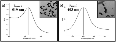 | ||
| Fig. 1 UV/Vis spectra and TEM pictures of as-obtained (a) gold and (b) silver nanoparticles. | ||
This strategy was effective in producing stable inks, however the high amount of polymer leads to NP-polymer composites in which the metal NPs are masked by the polymers and being less accessible for the catalytic applications. The dispersion in the particle size was monitored by UV/Vis spectroscopy of various NPs. An adequate stability and reproducibility was achieved for NPs with an average size of 30 nm (λmax = 403 nm) (Fig. 1(b)).22
The dispersion of the alloy-particles was green in colour, which was corroborative of the spectral maximum (λmax = 485 nm) observed in the UV/Vis data (Fig. 2(a)) and the formation of alloy particles.22 The absence of any other pronounced UV/Vis signature confirmed the formation of a homogenous alloy composition. Furthermore the measured maximum lies between the maxima observed for gold (λmax = 519 nm) and silver (λmax = 403 nm) particles. The TEM measurement showed spherical particles with sizes between 20–30 nm (Fig. 2(a)). The EDX analysis showed a higher content of gold (66.4%) than silver (33.6%) in the Au–Ag particles (Fig. 2(b)).
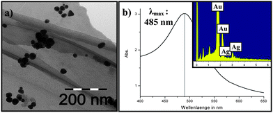 | ||
| Fig. 2 (a) TEM image, UV/Vis spectrum and (b) EDX analysis of Ag/Au alloy particles. | ||
II. CVD experiments on ink-jetted metal catalysts
Nanowires and nanotubes of different materials can be grown by the well-known vapour–liquid–solid (VLS) model, which uses metal particles as templates for guiding the growth of anisotropic one-dimensional structures. However, for a controlled growth, it is important to find new methods for positioning the catalysts on the substrates, because the commonly used sputtering and spin-on techniques offer only randomly grown nanostructures. The possibility of selectively positioning metal nanoparticles on a substrate was tested by printing inks of the Ag, Au, and Ag–Au alloy NPs synthesized in this work (Fig. 3).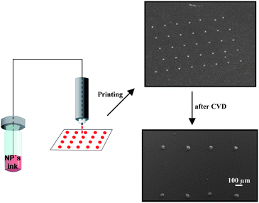 | ||
| Fig. 3 Procedure for inkjet printed substrates and following regioselective CVD experiments. | ||
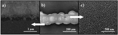
Fig. 4(a) shows a SEM image of printed Si(001) substrate, which was decorated with rows of Au nanoparticles to perform CVD of SnO2 nanowires.17 Also, compound substrates containing printed structures of Ag, Au and Ag–Au NPs were fabricated in order to evaluate the differential catalytic activities towards NW growth. The SEM micrograph of the Au decorated substrate revealed that the nanowire growth occurred preferentially and site-selective on the Au catalyst nanoparticles. A slight migration of gold clusters was observed which can be explained by the higher diffusion rate and the liquefied state of gold at the growth temperature (∼750 °C). Apparently, the presence of CMC as a steric stabilizer decreases the lateral mobility of Au NPs. On the other hand, the high degree of entanglement of Au NPs with the polymer leads to residual carbon that hampers the catalytic activity (Fig. 4(a)). The printing experiments with less viscous polyethylene glycol (PEG) instead of CMC led to a much faster evaporation process, which reduced the carbon contamination (Fig. 4(b)). Fig. 4(b) shows the SEM images of printed catalysts and the as-grown nanowires, which supports the concept of local and confined growth of nanowires by pre-positioning the metal catalyst particles. The coffee-drop effect caused by concentration gradient in aqueous micro-droplets of metal NPs could be overcome by mixing small amounts of polymeric additives.
 | ||
| Fig. 4 Inkjet printed dots after CVD experiment with Sn(OtBu)4 of (a) Ag, Au and alloy dispersions with added CMC and (b) Au dispersion with added PEG. | ||
Further, it was found that Ag and Au NPs show different catalytic activity due to intrinsic reactivity patterns as well as due to the dispersions in the particle sizes, which are more pronounced for the Ag species. This was verified by printing Ag, Au and Ag–Au alloy NPs on Si(001) substrates and by performing CVD under similar conditions. As expected, the density of as-grown nanowires followed the trend Au > Ag–Au > Ag. Further experiments to elucidate this aspect are currently under way.
The inkjet printing of metal NP dispersions is an interesting technique for rapid patterning of growth templates (catalysts), which can be applied to various substrates and allows to fabricate different patterns for the structural manipulation of CVD-grown nanostructures. Fig. 5 shows the scanning electron and optical micrograph of patterns obtained from Au@PEG inks. The distance between drops in a dot-matrix pattern could be varied from 80–500 μm, whereas the diameter of the drop ranged from 30 to 180 μm due to different surface energies of the substrates interacting with the ink.
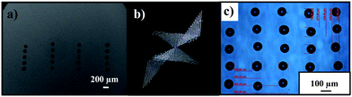 | ||
| Fig. 5 (a) Scanning electron and optical (b, c) micrographs of patterns printed by Au@PEG inks. | ||
III. CVD experiments on inkjet printed SAM
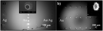
The hydrophilic surface obtained by treating Si(001) substrates in an oxygen plasma (1) was chemically modified by inkjet printing of an APTES monolayer (2), which was then exposed to a colloidal gold suspension (3) to regioselectively deposit the particles on the patterned areas (Fig. 6). Fig. 7(a) presents the SEM images of a printed Au@APTES line to elaborate the comparable density of gold NPs on the boundary (a) and in the middle of the monolayer (c). The dense-arrangement of NPs on the printed line of APTES leads to a continuous structure (c), which can be used for printing electronic circuits. When compared to the few particles present on the oxidized silicon surface, the printed area showed a strong interaction between the amine group of the linker and the gold NPs. The CVD experiments on Au NPs revealed the growth of nanowire arrays originating from the printed droplets only (Fig. 8). In addition, the regioselectivity was also demonstrated as (Fig. 8(b)) no diffusion of the Au NP beyond the printed structure was observed.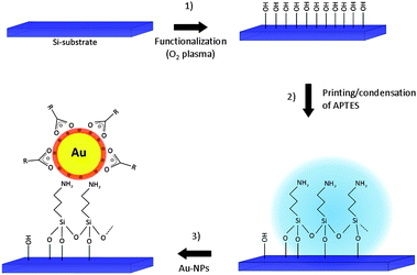 | ||
| Fig. 6 Schematic images showing the fabrication of the gold monolayer beginning from the silicon (001) substrate. | ||
 | ||
| Fig. 7 SEM images of a line pattern of nanoparticles monolayer achieved by inkjet printing of APTES linker. | ||
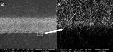 | ||
| Fig. 8 (a) SEM images of a line pattern of nanoparticles monolayer after CVD experiment with Sn(OtBu)4 with focusing on the border (b) to demonstrate the regioselective growing of SnO2 nanowire. | ||
Conclusions
We have demonstrated a cost-effective nanoparticle-based printing technique for a selective and pre-defined patterning of metal NPs, and have evaluated their use as catalysts in CVD processes to grow nanowires. Dispersion of Ag, Au and their alloy particles in polymers provided stable dispersions that were used as functional inks for fabricating diverse patterns. Major advantages of using NPs as pigments lies in the possibility of controlling the particle concentration in the inks, which ultimately determines the density and radial dimensions of nanowires. In addition, the site selective patterning of a SAM and subsequent attachment of printed NPs opens up new avenues for chemical fixation of the arrays of metal catalyst (and co-catalysts) on different substrates. The method is also feasible for the production of optoelectronic devices, where a selective bonding of SPR-active (SPR = Surface Plasmon Resonance) Au NPs is desired. Furthermore, the inkjet printing is a technically mature technology and offers the potential for volume production of printable devices such as sensors, photovoltaic and low-voltage batteries.Acknowledgements
Authors are thankful to the University of Cologne, Cologne Germany, the Federal Ministry of Education and Research (BMBF; KoLiWIn, 55102006) and the European Commission (for supporting this activity in the framework of the joint EU-Russia cooperation “S3”) for the financial support. Thanks are also due to Dr Hao Shen, Dr Lhoussaine Belkoura and Martin Hoffmann for electron microscopy.References
- P. Calvert, Chem. Mater., 2001, 13, 3299 CrossRef CAS.
- B.-J. de Gans, P. C. Duineveld and U. S. Schubert, Adv. Mater., 2004, 16, 203 CrossRef CAS.
- H. P. Le, J. Imaging Sci. Tech., 1998, 42, 49 Search PubMed.
- http://www.microdrop.de/ .
- D. Jang, D. Kim and J. Moon, Langmuir, 2009, 25, 2629 CrossRef CAS.
- R. S. Wagner and W. C. Ellis, Appl. Phys. Lett., 1964, 4, 89 CAS.
- H. Ago, K. Murata, M. Yumura, J. Yotani and S. Uemura, Appl. Phys. Lett., 2003, 82, 811 CrossRef CAS.
- R. Kitsomboonloha, S. Baruah, M. T. Z. Myint, V. Subramanian and J. Dutta, J. Cryst. Growth, 2009, 311, 2352 CrossRef CAS.
- J. Wang, T. Zhu, J. Song and Z. Liu, Thin Solid Films, 1998, 327–329, 591 CrossRef CAS.
- C. A. Goss, D. H. Charych and M. Majda, Anal. Chem., 1991, 63, 85 CrossRef CAS.
- S. Liu, T. Zhu, R. Hu and Z. Liu, Phys. Chem. Chem. Phys., 2002, 4, 6059 RSC.
- I. Riansaari, L. Walder, M. Burchardt, I. Zawisza and G. Wittstock, Langmuir, 2008, 24, 9110 CrossRef.
- A. N. Shipway, E. Katz and I. Willner, ChemPhysChem, 2000, 1, 18 CrossRef CAS.
- S. M. Sze, Semiconductor Devices, Wiley, New York, 2001 Search PubMed.
- G. S. V. Coles and G. Williams, J. Mater. Chem., 1992, 2, 23 RSC; S. Mathur and S. Barth, Small, 2007, 3, 2070 CrossRef CAS; Y. N. Xia, P. D. Yang, Y. G. Sun, Y. Y. Wu, B. Mayers, B. Gates, Y. D. Yin, F. Kim and H. Q. Yan, Adv. Mater., 2003, 15, 353 CrossRef CAS; E. Comini, C. Baratto, G. Faglia, M. Ferroni, A. Vomiero and G. Sberveglieri, Prog. Mater. Sci., 2009, 54, 1 CrossRef CAS; F. Hernández-Ramírez, A. Tarancón, O. Casals, J. Rodríguez, A. Romano-Rodríguez, J. R. Morante, S. Barth, S. Mathur, T. Y. Choi, D. Poulikakos, V. Callegari and P. M. Nellen, Nanotechnology, 2006, 17, 5577 CrossRef CAS; F. Hernández-Ramírez, J. D. Prades, A. Tarancón, S. Barth, O. Casals, R. Jiménez-Diaz, E. Pellicer, J. Rodríguez, M. A. Juli, A. Romano-Rodríguez, J. R. Morante, S. Mathur, A. Helwig, J. Spannhake and G. Mueller, Nanotechnology, 2007, 18, 495501 CrossRef; F. Hernández-Ramírez, A. Tarancón, O. Casals, E. Pellicer, J. Rodríguez, A. Romano-Rodríguez, J. R. Morante, S. Barth and S. Mathur, Adv. Funct. Mater., 2007, 10, 1191; Z. L. Wang, Mater. Today (Oxford, U.K.), 2004, June 26 Search PubMed.
- M. Law, H. Kind, B. Messer, F. Kim and P. D. Yang, Angew. Chem., 2002, 114, 2511 CrossRef.
- S. Mathur, S. Barth, H. Shen, J.-C. Pyun and U. Werner, Small, 2005, 1, 713 CrossRef CAS.
- J. Turkevic, P. C. Stevenson and J. Hillier, Discuss. Faraday Soc., 1951, 11, 55 RSC.
- S. Magdassi, A. Bassa, Y. Vinetsky and A. Kamyshny, Chem. Mater., 2003, 15, 2208 CrossRef CAS.
- R. D. Deegan, O. Bakajin, T. F. Dupont, G. Huber, S. R. Nagel and T. A. Witten, Nature, 1997, 389, 827 CrossRef CAS.
- M. J. Hampden-Smith, T. A. Wark, A. Rheingold and J. C. Huffman, Can. J. Chem., 1991, 69, 121 CAS.
- C. Noguez, J. Phys. Chem. C, 2007, 111, 3806 CrossRef CAS; S. Link and M. A. El-Sayed, J. Phys. Chem. B, 1999, 103, 8410 CrossRef CAS; C. N. R. Rao, A. Müller, A. K. Cheetham, Nanomaterials Chemistry, Wiley-VCH, Weinheim, 1st edn, 2007 Search PubMed.
| This journal is © The Royal Society of Chemistry 2010 |