DOI:
10.1039/C0NR00128G
(Paper)
Nanoscale, 2010,
2, 1128-1133
The influence of doping on the device characteristics of In0.5Ga0.5As/GaAs/Al0.2Ga0.8As quantum dots-in-a-well infrared photodetectors
Received
16th February 2010
, Accepted 7th April 2010
First published on
1st June 2010
Abstract
We report on a detailed analysis of the effects of doping on the main device parameters of In0.5Ga0.5As/GaAs/Al0.2Ga0.8As quantum dots-in-a-well infrared photodetectors. Due to the relatively large conduction band offset of GaAs/Al0.2Ga0.8As (167meV) transitions from wetting layer to quantum well states are observed for the highly doped devices. Since increasing the doping concentration fills the quantum dot states, electrons are forced to occupy the one-dimensional wetting layer states and therefore have quantum-well-like properties. This has facilitated a comparative study of the effects of three-dimensional and one-dimensional confinement of electrons on device parameters such as the responsivity and dark current by studying one particular detector structure with different doping concentrations of the active region.
1 Introduction
The dependence of quantum well infrared photodetector (QWIP) device parameters such as dark current and responsivity on the doping concentration of the active region is quite well understood. For example, the total optical absorption is proportional to the electron concentration of the quantum wells (QWs) since the optical dipole moment between the ground and excited state subbands are approximately independent of the shared in-plane k-vector of the initial and final states.1,2 QWIP dark current increases with doping and has a dependence that can be described in terms of the Fermi level.3 For typical QWIP doping concentrations, the Fermi level is approximately 10 meV above the QW conduction band edge.4
Much less is known about the effects that doping has upon quantum dot infrared photodetector (QDIP) device performance. The two main reasons for the lack of a general consensus are the more complicated effects of doping on QDIP behavior and the effects of doping are strongly dependent on the quantum dot (QD) band structure which varies significantly with each reported device. It is expected that QDIP dark current is very sensitive to the doping concentration since the Fermi level increases more dramatically with the QD electron occupation number due to state filling and the relatively large energy spacing between the QD excited and ground states.5 QD excited state wavefunctions can be very different from the ground state wavefunction so the absorption strength and spectrum can have a more complicated dependence on doping than the simple linear relationship of a QWIP.9 Also, photoconductive gain can depend on the QD electron occupation number since electron capture relies upon the availability of unoccupied states resulting in a more complicated relationship between responsivity and doping.
We have previously reported on an analysis of the properties of a set of In0.5Ga0.5As/GaAs/Al0.2Ga0.8As quantum dots-in-a-well (DWELL) infrared photodetectors including the effects of the QW thickness on the spectral response.6 In this paper we investigate in detail the relationship between the electron concentration of the active region and the main device parameters of a similar set of detectors.
2 Experimental details
A set of four DWELL photodetector devices consisting of 10 QD layers were grown that are identical apart from the doping concentration of the active region. Devices were grown using low-pressure metal–organic chemical vapor deposition (MOCVD) on (001) oriented semi-insulating GaAs substrates. A schematic of the device structure is shown in Fig. 1. In0.5Ga0.5As QDs formed from 5.7 monolayers of material are deposited on a 3 nm GaAs QW and capped with a 7 nm GaAs QW layer all grown at 550 °C. The barrier layers are 45 nm thick and consist of Al0.2Ga0.8As grown at the higher temperature of 650 °C. The growth parameters of In0.5Ga0.5As QDs grown on GaAs substrates have previously been optimized and have a high optical quality.7 Plane view transmission electron microscopy images of a single layer of QDs grown under the same conditions as the detectors indicate a QD density of 2 × 1010 cm−2. To supply the QDs with electrons the central 35 nm of all 45 nm Al0.2Ga0.8As barriers were doped with silicon atoms. To accurately determine the electron concentration of the QD layers, a number of doped Al0.2Ga0.8As epilayers were grown and Schottky contacts were formed by metal evaporation. Capacitance voltage measurements were then performed on the Schottky diodes to determine the carrier concentration of these epilayers. Assuming that all electrons provided by doping occupy the DWELL layers, the number of electrons per QD are 1, 3, 8 and 14 electrons/QD for devices A, B, C and D respectively. To further investigate the properties of the wetting layer (WL) electrons an additional device (device E) was grown and fabricated consisting of just a WL in a QW by depositing only 3.2 monolayers of In0.5Ga0.5As, but is otherwise identical to device D.
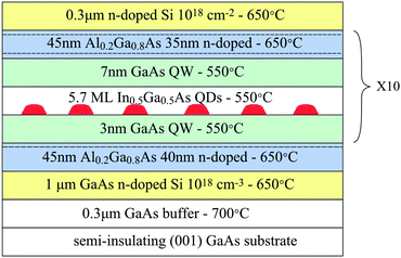 |
| | Fig. 1 Schematic of the quantum dots-in-a-well infrared photodetector devices grown by MOCVD. Also indicated are the temperatures at which the layers were grown. | |
After growth, wafers were processed into 250 μm square mesa devices by contact UV lithography and wet chemical etching. Bottom and 150 μm circular top ohmic contacts were formed by thermal evaporation of Ge/Au. Devices were then wire bonded into DIP packages for characterization.
3 Results and discussion
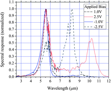
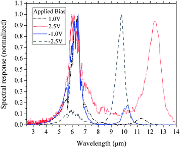
Photoluminescence (PL) measurements were performed on the wafers to confirm the QDs are optically active and have very low defect levels, the results of which are shown in Fig. 2. PL measurements also have the benefit of providing some information about the semiconductor band structure. All devices displayed a strong PL signal with small variations in the peak energy which is typically observed due to small unintentional changes in the QD growth conditions. Two peaks in the PL spectra are evident which are attributed to the QD ground state (1.16 eV) and WL (1.29 eV) electron–hole recombination. The first task in analyzing the effects of the doping concentration on the performance characteristics of these detectors is the construction of a conduction band diagram of the DWELL region. For this, PL and spectral response measurements and numerical calculations are used. The spectral response of all devices are shown in Figs. 3, 4, 5 and 6 for different biases (bias potentials are with respect to the bottom contact layer). All devices display very similar spectral responses with a mid-wavelength infrared (MWIR) peak at 5.6 μm and a long wavelength infrared (LWIR) peak with a bias dependent position within 8 to 10 μm. For all devices the LWIR peaks appear for biases greater than about 1.5 V with some fairly small variations in their onset, particularly device A which requires approximately an extra 0.5 V for the LWIR response.
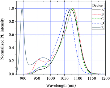 |
| | Fig. 2 77 K photoluminescence response of all the photodetector devices. The peaks at about 1070 nm are the emission from the QD electron–hole ground state recombination and the WL emission is seen at 960 nm for devices A–D and 895 nm for device E. | |
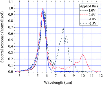 |
| | Fig. 3 77 K normal incidence spectral response of device A (1e/QD). | |
 |
| | Fig. 4 77 K normal incidence spectral response of device B (3e/QD). | |
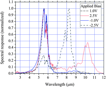 |
| | Fig. 5 77 K normal incidence spectral response of device C (8e/QD). | |
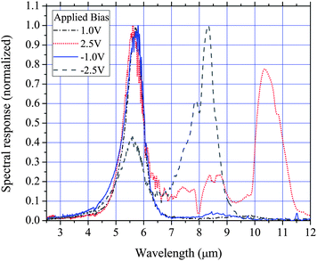 |
| | Fig. 6 77 K normal incidence spectral response of device D (14e/QD). | |
Experimental data and calculations suggest that the 5.6 μm peak is due to transitions from the QD ground state to the first excited state of the combined QD/QW. The transition is a response to z-polarized (growth direction) radiation and the energy is dependent on the thickness of the AlGaAs/GaAs QW.6 Since the minimum energy for a z-polarized transition from the QD ground state is 5.6 μm the LWIR peaks must either be a response to x–y polarized light or are a result of transitions from excited states. Numerical calculations show that normal incidence absorption from the QD ground state to states beyond the QD first excited state with an energy of about 10 μm is possible for QDs with a small confinement energy. However, the polarization dependent spectral response measurements of device A shown in Fig. 7 reveal that the LWIR peaks are a response to z-polarized (growth direction) radiation. Calculations indicate that the long wavelength peaks are due to WL-to-QW transitions. The large voltage dependence of the spectral peak position is due to a linear Stark effect term resulting from the spatial offset of the WL ground state and QW excited state wavefunctions. The offset of the wavefunctions occurs because of the asymmetric position of the WL in the QW.
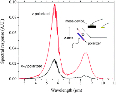 |
| | Fig. 7 77 K polarized spectral response of device D. Light is passed through a polarizer and is incident upon the back of the wafer polished at an angle of 45°. | |
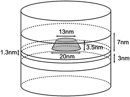
To provide a clearer understanding of the band structure and the transition energies numerical calculations have been performed. Within the single-band effective mass model the energy levels and absorption cross section of the DWELL structure have been calculated. The effects of the QD strain acting through the conduction band deformation parameters has been taken into consideration by solving finite element routines of the elastic continuum model. The correction to the conduction band potential is ΔV(r) = ac(r)ehy(r), where ac(r) is the conduction band deformation parameter and ehy(r) is the hydrostatic component of the strain. Providing the parameters shown in Table 1 as input and assuming the cylindrically symmetric DWELL geometry shown in Fig. 10 the absorption spectrum has been calculated for various electric fields as shown in Fig. 11. For the calculation of the WL absorption spectrum a one-dimensional structure consisting of a WL-in-a-well is modeled using the same parameters as the DWELL structure. From the calculated eigenstates the absorption cross section is found by applying Fermi's rule within the dipole approximation. To represent the effects of the QD size variations, intersubband transitions have been broadened by replacing the delta function of Fermi's rule with the Gaussian,
| | 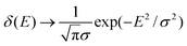 | (1) |
where
σ which determines the energy width, is set to a value that gives a FWHM of 20 meV.
Table 1 Single-band effective mass material parameters used in the numerical calculations of QD absorption cross section. ac is the conduction band deformation parameter and EM is the effective mass
|
|
EM (m*/me) |
Unstrained potential/eV |
a
c/eV |
| QD |
0.05 |
−0.702 |
−6.13 |
| QW |
0.067 |
−0.167 |
−7.17 |
| WL |
0.05 |
−0.702 |
−6.13 |
| Barrier |
0.083 |
0.0 |
−6.86 |
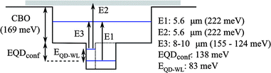
The calculated absorption cross section spectrum is in good agreement with the measurements including the electric field dependence of the LWIR peaks. In addition the calculations predict that there is a small but significant WL-to-continuum absorption, the strength of which is dependent on the asymmetric position of the WL in the QW and is in general weaker than the WL-to-QW transition. The spectral response of device E, shown in Fig. 8, confirms the nature of transitions from the WL. The peaks of device E are red-shifted compared with the other devices due to the increased ground state energy of the thinner WL as indicated by the PL measurements (Fig. 2). The spectral response of device E confirms that the 5.6 μm peak of the other devices is due to both QD-to-QW and WL-to-barrier continuum transitions and that larger biases are required to extract electrons from the QW states. For all devices the relative strength of the MWIR and LWIR responses have a weaker bias dependence for biases greater than about |V| > 3.0V. For such large biases the escape probability of electrons excited to QW states must be near unity and therefore changes in voltage have a much weaker influence on the relative response of the two peaks. A band diagram displaying the relevant energy levels and transitions is shown in Fig. 9. The value derived for the QD confinement energy EQD is based on the PL measurements and previous studies of InGaAs/GaAs QDIPs which consist of QDs grown under the same conditions are the devices studied here.8
 |
| | Fig. 8 77 K normal incidence spectral response of device E. | |
 |
| | Fig. 9 Simplified conduction band diagram of the quantum dots-in-a-well structures displaying the relevant optical transition energies (E1, E2 and E3) and the energies of the QD and WL ground states with respect to the unstrained GaAs conduction band edge. | |
 |
| | Fig. 10 QD simulation domain displaying the dimensions assumed for numerical calculations. | |
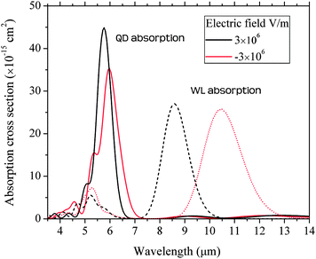 |
| | Fig. 11 Absorption cross section calculation results of the DWELL structure. Shown are the absorption spectra for an electron in the QD ground state and an electron in the WL ground state. | |
In addition to transitions from the QD ground state there is the possibility of transitions from QD excited states. The QD ground state to WL band edge energy separation is only about 80 meV. The first excited state for a single electron in a QD is about 50 meV as determined by calculation, a value that is consistent with typical measurements. Considering the electron–electron interaction energy it is unlikely that the QDs will accommodate more than a few electrons. Therefore transitions from the QD first excited state are the most relevant. Numerical calculations of the absorption spectrum of an electron in the QD first excited state due to z-polarized light have a similar spectral peak energy to the calculated absorption spectrum of QD ground state electrons. This is in part due to the fact that the QD-to-QW transition energy is much larger than the QD and WL energy separation, EQD–WL. Therefore the combined absorption of the QD ground and excited states remains a single peak at about 5.6 μm.
Although device A has a small doping concentration that should result in the occupation of only the QD ground state at low temperature, there is a large WL-to-QW response for larger applied biases. The most likely cause of the population of WL states of devices A and B is charge accumulation through the injection of electrons from the emitter contact layer. Charge accumulation or depletion of the device active region is a function of the relative electric field dependence of carrier injection from the emitter contact and the extraction of carriers from bound states.3 Explicit calculations of charge accumulation in QDIPs show that an increase in the QD electron occupation number is expected.10,11 Usually the QD density of QDIPs is relatively small compared with the typical electron sheet concentration of QWIPs, and therefore any charge accumulation would have a greater effect on the former.
To determine the magnitude of the photoresponse normal incidence integrated responsivity measurements were performed, the results of which are shown in Fig. 12. The integrated responsivity measurements were performed by irradiating the detectors with an 800 °C blackbody radiation source chopped at 140 Hz. The responsivity is calculated by integrating the spectral exitance of the blackbody source, Mq(λ), multiplied by the normalized spectral response of the detector, ![[S with combining macron]](https://www.rsc.org/images/entities/i_char_0053_0304.gif) (λ), to give an effective radiation power, Eq,
(λ), to give an effective radiation power, Eq,
| | 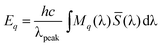 | (2) |
where
λpeak is the wavelength of the spectral response peak of the photodetector.
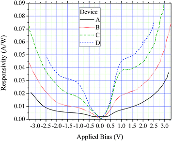 |
| | Fig. 12 77 K normal incidence responsivity of all devices as a function of applied bias for the 5.6 μm peak. | |
The responsivity, Rp, is then determined from
| |  | (3) |
where
Iphoto is the measured photocurrent due to changes in the incident radiation power reaching the
detector because of the action of the chopper. To prevent
interband transitions from interfering with the measurements a
germanium block was placed in the radiation path to absorb short-wavelength radiation. The incident radiation power is given by,
| |  | (4) |
where
D is the distance from the blackbody source exit to the photodetector and
d is the diameter of the blackbody opening.
TGe is the transmission of the
IR radiation through the germanium filter and
TBaF is the transmission through the BaF
2 window of the 77 K dewar.
Fchopper is the fundamental harmonic component of the square wave chopping function and has the value of 0.45 and
Adet is the active area of the photodetector. For all responsivity measurements the normalized
spectra (
λ) used in the calculations are taken only at a single bias with a small magnitude such that the LWIR peaks are not present.
The responsivity does not show a linear dependence on the doping concentration which is the typical case for QDIPs due to the different absorption coefficients of the various transitions and escape probabilities of excited states. Table 2 summarizes the relative responsivities of the devices for various biases. From the spectral response data of all devices it is evident that WL-to-QW transitions do not contribute to the responsivity for biases less than about 2 V. However, it is harder to determine the responsivity due to the QD-to-QW transitions since their effect on the photoresponse cannot be separated from the WL-to-continuum transitions. For small applied biases essentially all electrons in the active region of device A should be in QD states and therefore the responsivity would largely be due to the QD-to-QW transition. Since the responsivity of device A for small biases is large considering the smaller doping concentration it is likely that the QD-to-QW transition has a larger escape probability than the WL-to-QW transition. In addition the strength of the QD-to-QW absorption is greater than the WL-to-continuum absorption which would further enhance the responsivity of device A. It is interesting to compare the devices studied here to the voltage dependence of the responsivity of other QDIPs with excited states that are confined well below the conduction band edge. Krishna reports a significant 7.5 μm photoresponse at moderate biases for a DWELL detector with an excited state confined approximately 90 meV below the conduction band edge.12 This tends to indicate that the QD excited states have a greater escape probability which is possibly due to a longer QD excited state lifetime.
Table 2 Relative normal incidence 77 K integrated responsivity of all devices (photocurrent/optical power) for various applied biases. Also indicated are the number of electrons per QD for each device. The responsivities are for the 5.6 μm peak
| Device |
Bias/V |
N° e− per QD |
| 0.5 |
−0.5 |
1.0 |
−1.0 |
| A |
0.23 |
0.26 |
0.16 |
0.17 |
1 |
| B |
0.51 |
0.48 |
0.41 |
0.33 |
3 |
| C |
0.89 |
0.78 |
0.84 |
0.61 |
8 |
| D |
1.0 |
1.0 |
1.0 |
1.0 |
14 |
To investigate the relationship between the carrier concentration and the dark current of the photodetectors, current–voltage measurements were performed for device temperatures between 10–200 K. Devices were mounted onto an aluminium finger of a closed cycle helium flow cryostat and were shielded from the room-temperature background radiation by a cold shield. The relative dark currents of all devices for various temperatures are shown in Fig. 13 and the activation energies are shown in Fig. 14. The dark current activation energies are found to increase with temperature since at lower temperatures electrons tend to tunnel from states further below the barrier band edge. Therefore a narrower temperature range of 110–130 K was used to determine the activation energies which better reflects the dark current mechanisms within this temperature range. The activation energy decreases with an increasing doping concentration and as a result the dark current magnitude increases. At low temperature, the increase in the Fermi level with doping is more rapid at the lower doping concentrations due to the filling of the QD states. Due to the larger density of states of the WL, further increases of doping has a smaller impact on the Fermi level. The dark current magnitude of all devices is found to be roughly proportional to the factor exp(−Ea/kBT), where Ea is the activation energy and T is the device temperature. Therefore it is only the energy of occupied states that determines the dark current magnitude and not the dimensionality of the confinement for the devices reported here.
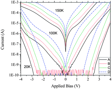 |
| | Fig. 13 The dark current magnitude of all devices as a function of applied bias for various temperatures. | |
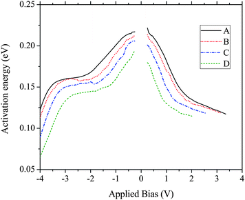 |
| | Fig. 14 The dark current activation energy of all devices as a function of applied bias, calculated with device temperatures within the 110–130 K temperature region. | |
4 Conclusion
In conclusion the relationship between the doping concentration of the active region and the device parameters of In0.5Ga0.5As/GaAs/Al0.2Ga0.8As DWELL photodetectors has been investigated. It has been found that responsivity is not proportional to the doping concentration due to the different absorption strengths of the various energy levels that are occupied as QD states are filled with an increasing electron concentration. This is expected to be a general result for QDIPs since filling a QD with electrons beyond the ground state (2e/QD) will result in the additional electrons occupying higher energy states which will have dominant transitions red shifted from the transitions associated with the QD ground state electrons. The QD electron occupation number has been found to be very dependent on the applied bias due to charge accumulation from the electrons injected from the emitter contact layer. Charge accumulation is expected to play a greater role for InGaAs/GaAs based QDIPs than for most QWIPs reported in the literature. This is because of the relatively small QD density and the fact that electrons tend to be more readily injected from the emitter contact of QDIPs since the barrier and the heavily doped emitter contact are of the same material (GaAs). The relative device dark currents are found to be approximately proportional to the factor exp(−Ea/kBT), where Ea is the activation energy and T is the device temperature suggesting that the energy of occupied states is the dominant factor determining the dark current rather than the density of the occupied states. If QDIP or DWELL dark current originates from the scattering of electrons from WL or QW states to barrier continuum states then the dark current could be more dependent on the occupation of the two-dimensional density of states which could be near thermal equilibrium, rather than the rate of electrons scattering from QD states.
Acknowledgments
Thanks are due to Michael Aggett and Craig Saint for expert technical advice. The Australian Research Council is gratefully acknowledged for financial support. The Australian National Fabrication Facility, established under the Australian Government National Cooperative Research Infrastructure Strategy, is acknowledged for access to the facilities used in this work.
References
- S. D. Gunapala, B. F. Levine, L. Pfeiffer and K. West, J. Appl. Phys., 1991, 69, 6517 CrossRef CAS
 .
.
- Y. Yang, H. C. Liu, W. Z. Shen, N. Li, W. Lu, Z. R. Wasilewski and M. Buchanan, IEEE J. Quantum Electron., 2009, 45, 623–628 CrossRef CAS .
- J. L. Pan and C. G. Fonstad Jr., Mater. Sci. Eng., R, 2000, 28, 65–147 CrossRef .
- K. K. Choi, C. Y. Lee, M. Z. Tidrow, W. H. Chang and S. D. Gunapala, Appl. Phys. Lett., 1994, 65, 1703 CrossRef CAS .
- K. Drozdowicz-Tomsia, E. M. Goldys, L. Fu and C. Jagadish, Appl. Phys. Lett., 2006, 89, 113510 CrossRef .
- G. Jolley, L. Fu, H. H. Tan and C. Jagadish, J. Phys. D: Appl. Phys., 2009, 42, 095101 CrossRef .
- P. Lever, H. H. Tan and C. Jagadish, J. Appl. Phys., 2004, 95, 5710–5714 CrossRef CAS .
- L. Fu, I. McKerracher, H. H. Tan and C. Jagadish, Appl. Phys. Lett., 2007, 91, 073515 CrossRef .
- R. S. Attaluri, S. Annamalai, K. T. Posani, A. Stintz and S. Krishna, J. Appl. Phys., 2006, 99, 083105 CrossRef .
- V. Ryzhii, I. Khmyrova, V. Pipa, V. Mitin and M. Willander, Semicond. Sci. Technol., 2001, 16, 331–338 CrossRef CAS .
- M. A. Naser, M. J. Deen and D. A. Thompson, J. Appl. Phys., 2008, 104, 014511 CrossRef .
- S. Krishna, J. Phys. D: Appl. Phys., 2005, 38, 2142–2150 CrossRef CAS .
|
| This journal is © The Royal Society of Chemistry 2010 |
Click here to see how this site uses Cookies. View our privacy policy here.