Doping single-walled carbon nanotubes through molecular charge-transfer: a theoretical study
Arun K.
Manna
and
Swapan K.
Pati
*
Theoretical Sciences Unit, Jawaharlal Nehru Center for Advanced Scientific Research, Jakkur Campus, Bangalore-560064, India. E-mail: pati@jncasr.ac.in; Fax: +91 80 2208 2766/2767; Tel: +91 80 2208 2839
First published on 14th April 2010
Abstract
We study the effect of the molecular charge transfer on the electronic structure of metallic (5,5) and semiconducting (8,0) single-walled carbon nanotubes (SWNTs) induced by surface adsorption of various organic donor–acceptor molecules of different affinities using ab initio density functional theory. Our results, obtained from first-principles spin-polarized calculations show that the adsorption of molecules with different affinities reflects the difference in interaction strength that measure the overall energy of adsorption. Moderate values of the binding energy of these surface adsorbed molecular charge-transfer complexes suggest that the nature of interaction is in the physisorption regime, and mainly governs by Coulombic forces. We also find that the large band gap of semiconducting (8,0) SWNT can be tuned through the surface adsorption of selective organic molecules which gives rise to mid-gap localized molecular levels near the Fermi energy with tuning of band gap region. Interestingly, we find that the metallic (5,5) SWNT and semiconducting (8,0) SWNT turn into semiconducting and metallic nanotubes respectively in presence of selective surface adsorbed molecules, corroborating recent experimental findings. We also suggest that these charge transfer effect can be probed through optical conductivity measurement, as the low-frequency profiles are affected by charge transfer.
1. Introduction
Owing to their outstanding mechanical and opto-electronic properties, the low-dimensional carbon nanomaterials have been the focus of extensive research in this era of miniaturized electronic devices. Among the carbon nano structures, the single-walled carbon nanotubes (SWNTs) are quite fascinating because of their novel mechanical, electrical and opto-electronic properties with huge potential applications in nano electronic devices.1–7 The SWNTs are one dimensional (1D) carbon systems with different chiralities and diameters. In addition to their inherent nanometre sizes, depending on their chirality and diameter, the SWNTs present either as a metallic or semiconducting character. Due to their special intriguing electronic and structural properties, these systems are considered as promising candidates for building a new area in technologies ranging from nanoelectronics,4–6 actuators,8 chemical sensors,9,10 DNA hybridization,11 and single-stranded DNA (ss-DNA) coated SWNT field effect transistor,10–12 among others.Electronic properties of low dimensional materials are mainly governed by their size, geometry and the carrier type and concentrations. Possibility of controlled way of transition from insulators through semiconductors to conductors, 1D SWNTs, are of practical interest in nano-science and nano-technology. The carriers present in SWNTs are strictly confined in 1D resulting in very high carrier mobilities. Moreover, it has been shown that electron or hole mobility can be controlled by tuning external electric field in nanotube based field effect devices.13–15 The similar observation was also made in case of graphene, thereby modulating its intriguing electronic properties.2 Furthermore, the utilization of spin components in SWNTs and graphene based electronic devices depends on the extent of spin polarization.16–18 In this respect, half-metallic materials show zero band gap for electrons with one spin orientation and insulating or semiconducting band gap for the other, resulting in a completely spin polarized current.19–25 In fact, spin polarization is the key foundation for spintronic device fabrication.
In fact, appropriate controlling and/or tuning of the electronic properties of 1D SWNTs, has numerous applications in designing of advanced electronic devices. However, the precise control of the carrier type and concentration has been achieved only recently, by electro-chemical doping,26 and through chemical modifications.27–30 Significant changes in the properties of these lower dimensional materials, in particular its phonon frequencies and electronic structure, are reported to occur when electrons or holes are added by electrochemical means.26 In fact, it has been reported that through electrochemical top-gating, it is possible to achieve a high level of doping.26,32,33 On the other hand, charge transfer is well known in molecular systems. This can be achieved either by intramolecular or by intermolecular charge-transfer pathway. For the intramolecular case, the donor and/or acceptor molecule has to form a new chemical bond with the nanotubes. Obviously, the formation of new covalent bonds through functionalizations of nanotubes may significantly modify the structure as well as its electronic properties. On contrary to that, one can self assemble some selective donor or acceptor molecules on the surface of SWNTs developing a possibility of through space charge-transfer. Recently, a number of controlled studies have been performed on 1D SWNTs and 2D graphene through chemical modifications;27,29,30 by adsorbing various organic molecules onto SWNTs and graphene surface where either electrons or holes are added to the system through molecular charge transfer. Such controlled adsorption of molecules induces charge transfer, which in turn greatly changes the electronic properties of nanotubes and graphene, in particular the characteristic Raman spectra. In fact, with variation in concentrations and nature of dopant molecules, it has been shown that the molecular charge-transfer affects the Raman frequencies as well as intensities in SWNTs giving rise to a tunable 1D electronic devices.27,30 These experiments28,29 and our earlier studies on graphene31 motivate us to perform a detail theoretical study on molecular charge-transfer interactions with SWNTs of various chiralities. The advantage of molecular doping over other means is to obtain a homogeneous electronic system with less charge impurities available for scattering, which infact responsible for reduction of carrier's speed. In fact, as like in SWNTs, the adsorption and intercalation of electron donors and acceptors on fullerene and graphene have also been achieved.29,31,34–42 Furthermore, there exists experimental reports providing heat of adsorption on various surfaces to assess the intrinsic affinities of different molecules. In fact, a prior knowledge of that together with chemical intuition will guide one for pursuing selection of appropriate adsorbate molecules for adsorption on various surfaces. The prediction of intrinsic mechanism of molecular adsorption requires not only the understanding of how the basic core interacts with the SWNTs surface but also the effect of substituents associated with the adsorbed molecules, highlighting the role of π–π interactions between the adsorbed molecules and SWNTs.
The purpose of our present study is to present a systematic and comprehensive analysis of the change in the electronic properties of donor- and acceptor-adsorbed SWNTs by using first principle calculations. We have considered a few representative donor and acceptor molecules with high affinities of electron-withdrawing and donating power. Tetracyanoethylene (TCNE), tetracyanoquinodimethane (TCNQ) are chosen as electron acceptors, and tetrathiafulvalene (TTF) as the electron donor. We have also considered two distinct SWNTs of different chirality having almost similar diameter so that the curvature effect can be neglected; a metallic, (5,5) SWNT and another semiconducting, (8,0) SWNT. Our results suggest that the donors and acceptors are adsorbed on SWNTs surface through a physisorption process. An analysis of Mülliken population predicts that the charge carriers are redistributed in nanotubes as well as in adsorbed molecules. The band structures together with density of states (DOS) analysis clearly show the appearance of discrete localized molecular levels in between valence and conduction bands near the Fermi level. Interestingly, our study shows that the surface adsorption of selective organic electron-donor and acceptor molecules on SWNTs of various chiralities can indeed tune its electronic properties from metallic to semiconducting state or vice versa with tuning of band gap region. We have also calculated the low frequency optical conductivity of these comparatively weakly bound physisorbed systems. Our theoretical results compare fairly well with recently reported experimental studies of molecular charge transfer on graphene and SWNTs.28,29,31,43
2. Computational details
The first-principle calculations are carried out using the linear combination of atomic orbital density-functional theory (DFT) methods as implemented in the SIESTA package.44 The generalized gradient approximation (GGA) in the Perdew–Burke–Ernzerhof (PBE) form45 and double ζ polarized (DZP) basis set are chosen for the spin-polarized DFT calculations. The interaction between ionic cores and valence electrons is described by norm conserving pseudopotentials46 in the fully non-local Kleinman-Bylander form.47 The pseudopotentials are constructed from 1, 4, 5, and 6 valence electrons for the H, C, N and S atoms, respectively. A reasonable mesh cut off of 300 Ry for the grid integration is utilized to represent the charge density. For full relaxation of all systems, we have sampled the Brilliouin zone by 1 × 1 × 40 k-points using the Monkhorst–Pack scheme whereas for electronic properties calculations, the Brilliouin zone is sampled by 1 × 1 × 80 k-points. The optimal atomic positions are determined until the magnitude of the forces acting on all atoms is less than 0.04 eV Å−1. Charge Transfer and chemical bonds are, in most cases, well described within DFT with either the local-density approximation (LDA) or the GGA to account for the exchange and correlation energy of the electrons.48 In addition to that, GGA approximation takes into account the semi-local exchange correlations which have significant impact on low-dimensional spin systems like graphene and carbon nanotubes. Since local density approximation overestimates the adsorption energy for these weakly bound systems,49 we have considered GGA to be an appropriate choice for describing interaction of either donor or acceptor with the large sp2 π surface of SWNTs.Periodic boundary conditions and a supercell approximation with a lateral separation of 12 Å between the adsorbed molecules are used to ensure that the interactions between molecule and their periodic images are negligible. The supercell (1 × 1 × 5) and (1 × 1 × 6) containing 160 carbon atoms of (8,0) SWNT and 120 carbon atoms of (5,5) SWNT are used for the electronic structure calculations. It is necessary to ensure that the x-and y-axes of the periodic supercells are large enough so that there is negligible interaction between adsorbed molecules with adjacent supercell. A distance of 20 Å along the x-and y-axes is found to be sufficient to ensure the energy convergence for configurations shown in Fig. 1. The presence of large curved surface area and the negligibly small decrease in adsorption energy while going from one to two number of adsorbate molecules lead us to consider two molecules adsorbed oppositely to the nanotube surface per supercell.
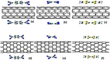 | ||
| Fig. 1 Side view of optimized structures for (a) (5,5) SWNT@2TCNQ, (b) (5,5) SWNT@2TCNE, (c) (5,5) SWNT@2TTF, and (d) (8,0) SWNT@2TCNQ, (e) (8,0) SWNT@2TCNE, (f) (8,0) SWNT@2TTF systems. The yellow, blue, grey and white color atoms correspond to sulfur, nitrogen, carbon and hydrogen respectively. | ||
3. Results and discussions
The relative stability of adsorbate-nanotube systems is determined by the adsorption energies. As it is well known, larger the adsorption energy, stronger is the binding of the adsorbate to the nanotube surface. The adsorption energy per adsorbate molecule is calculated by subtracting the energy of the optimized isolated molecule, Emolecule and the optimized equilibrium energy of the adsorbent, E(n,m) SWNT, from the total energy of the optimized molecule-(n,m) SWNT system, Emolecule+(n,m) SWNT, i.e.,| ΔEadsorption = [Emolecule+(n,m)SWNT − E(n,m)SWNT − n * Emolecule]/n | (1) |
A summary of the results for the fully optimized structures for all six systems are provided in Table 1. As can be seen, the distance between SWNT and the molecule remain at about 2.9–3.0 Å. The equilibrium adsorption distances are measured as the shortest distance between nanotube and adsorbed molecule. It can be easily seen from the Table 1 that for adsorption of TCNE on both nanotubes, the distances are relatively shorter as expected from its smaller molecular size with significant amount of charge transfer. It is also clear that the equilibrium adsorption distances are comparatively smaller than that observed for molecules adsorbed on graphene surface.31 It is to be noted that for TCNE and TCNQ adsorbed on both types SWNT, the sorbed molecule gets deformed at the –CN group side, while for TTF, the minimum energy configuration is the perfect planar conformation with respect to the nanotube surface. Moreover, the adsorption energies are comparatively smaller than those obtained for same molecules adsorption onto graphene surface.31 The reason of having lesser values of adsorption energy is due to the curved surface of SWNTs compared to flat planar graphene surface. The stability of these physisorbed SWNT-molecule complexes are due to the interactions of various length scales including Coulombic as evidenced from finite charge transfer. Also as can be seen, for all the six cases, the interaction is weak in agreement with moderate values of adsorption energy (see Table 1). The relatively larger value of adsorption energy for TCNQ compared to TCNE, is attributed to the fact that for TCNQ, the benzenoid structure provides a significant π surface for adsorption on SWNTs. This increases the extent of charge-transfer which in turn leads to gain the stability through electrostatic forces. Notably, the change in bond length alteration (BLA) reveals that the quinonoid form of TCNQ in its pure free gaseous state transform into benzenoid form on interacting with nanotubes. In comparison to TCNQ, the absence of large conjugated π surface with lesser amount of charge-transfer indicates that both electrostatic as well as van der Waals forces are, however, comparatively small for TTF molecule adsorbed on SWNTs. Interestingly, electron withdrawing adsorbates interact more specifically with metallic (5,5) SWNT compared to the semiconducting (8,0) SWNT with greater amount of charge transfer, resulting in larger values of adsorption energy. On the contrary, in case of electron-donating molecules, the results are exactly opposite with comparatively larger adsorption energy with semiconducting SWNTs. These findings are well consistent with the recent experimental results obtained by Rao et al.29
| SWNT-molecule complex | ΔEadsorption/kcal mol−1 | Distance/Å | Charge Transfer [e] |
|---|---|---|---|
| (5,5) SWNT@2TCNQ | −38.68 | 3.06 | −0.41 |
| (5,5) SWNT@2TCNE | −27.08 | 2.96 | −0.35 |
| (5,5) SWNT@2TTF | −27.31 | 3.09 | +0.08 |
| (8,0) SWNT@2TCNQ | −31.32 | 3.11 | −0.33 |
| (8,0) SWNT@2TCNE | −25.54 | 2.82 | −0.26 |
| (8,0) SWNT@2TTF | −29.61 | 2.95 | +0.17 |
An analysis of Mülliken population suggests that there is an effective charge transfer between the adsorbed molecule and SWNT. For both TCNE and TCNQ adsorbed onto metallic (5,5) SWNT, the extent of electron transfer from nanotube to adsorbed molecules are found to be ∼ 0.35 e and ∼ 0.41 e, respectively, while for the adsorption on semiconducting (8,0) SWNT, the values are ∼ 0.26 e, and ∼ 0.33 e, respectively, per sorbed molecule, per supercell. This is consistent with the nature of electron-withdrawing tendency of these molecules. For electron donor TTF, electron transfer of ∼ 0.08 e and ∼ 0.17 e are found from molecule to (5,5) SWNT and (8,0) SWNT, respectively, per sorbed molecule, per supercell. To understand whether the charge transfer accompanies spin moments, we have calculated the difference spin-density (i.e. up-spin–down-spin densities). Interestingly, we find that for TCNQ molecule adsorbed on semiconducting (8,0) SWNTs, there is accumulation of small but finite magnetic moment in nanotubes. For TCNE, however, there is a finite spin density in the molecule although nanotube remains nonmagnetic. In case of TTF, the hole carries no magnetic moment and both nanotube and the molecule remain nonmagnetic. Note that, for electron acceptor molecules (TCNE and TCNQ) adsorbed on SWNTs, the interaction is mainly electrostatic in nature as found from significant charge-transfer with definite spin moments. In fact, TCNQ, being the stronger electron acceptor in comparison to TCNE, the effect is more, similar to its adsorption on a Ag(100) and graphene surface.50,31 Incidentally, the charge transfer between nanotube and adsorbed molecule results in electrostatic attraction and thereby formation of a charge-transfer complex, in agreement with recent experimental results.28,29 The majority spin density is mainly localized on the sp2 carbon and nitrogen atoms for both TCNE and TCNQ adsorbed SWNTs, while the minority-spin density is localized on the sp carbon atoms of cyano groups present in acceptor molecules. Because of weak interactions through pz orbitals of TCNQ and its strong hole doping nature compared to TCNE with SWNTs, the latter contributes less to the overall spin, as noted earlier. Moreover, the excess transfered charge is mainly localized on the “N” atoms of the electron-withdrawing cyano group of both TCNE and TCNQ molecules, while for TTF adsorption, the relatively lesser extent of charge depletion from “S” atoms gives rise to moderate values of adsorption energy. We, however, would like to point out that our results on the amount of charge-transfer obtained through Mülliken population analysis are probably qualitatively correct, as the SIESTA-2.0 code, employed in the present study, does not include van der Waals interaction properly.
Additionally, for the nature of charge-transfer mechanism, after full relaxation, we perform a sequence of static calculations to compute the interaction energies between adsorbate molecules and SWNTs. For this, adsorbates are kept fixed at different distances along a line normal to the SWNTs axis. For each adsorbate, we perform calculation using eqn (1) to determine the interaction energy. The inverse distance variation of the interaction energy show nearly linear behavior with a small deviation at large distances. This proves conclusively that the charge transfer occurs through Coulombic forces, as was the case for graphene-donor or acceptor31 complex and even for the carbon nanotube-metal nanoparticle adsorption.36
To understand the effect of molecule-SWNT interaction on electronic structure, we plot band diagrams and corresponding DOS in Fig. 2 and Fig. 3, respectively. The band structures around the Fermi energy are significantly affected by molecular adsorption in both types SWNTs. For pure 1D metallic (5,5) SWNT, a flat spin-polarized DOS present exactly at Fermi level resembling the metallic state, however, there is no net spin-polarization (see Fig. 2(a)). In case of pure 1D (8,0) SWNT, a semiconducting band gap of ∼ 0.55 eV appears at the Fermi energy. The calculated DOS of SWNTs in presence of donor and acceptor adsorbates clearly show discrete molecular levels around the Fermi energy. The presence of flat molecular levels of TCNE and TCNQ in charge-transfer physisorbed systems at slightly above the Fermi level give rise to finite DOS for the molecule-nanotube complexes. In case of TTF adsorbed SWNTs, a flat band arises slightly below the Fermi level, resulting in finite DOS for the composites. In the latter case, both majority and minority spins are affected in exactly same manner with negligible amount of molecular charge-transfer. Also note that, in all the six molecule-SWNT complexes, the Fermi level shifts from its original position i.e. from its pure states. Interestingly, however, we find that in case of TCNE and TCNQ adsorbates, the electrons are removed from the SWNTs, depleting electron cloud from the uppermost valence bands of the later, with Fermi energy shifting towards the valance band. The effect is more pronounced for metallic (5,5) SWNT compared to the semiconducting (8,0) SWNT as the former has more carriers than the later. On the other hand, the accumulation of electrons cause shifting of the Fermi level towards the conduction band for TTF intercalated SWNTs. Note that, in a strict sense, the completely pure band picture of SWNTs near to the Fermi level is absent in SWNT-molecule complexes. Instead, as shown in Fig. 2, the hybridization of SWNT band and discrete molecular level results in disappearance of pure band picture for the charge-transfer complexes. Interestingly, for electrochemical top-gating study, the pure dispersive bands near the Fermi level remains unaltered even after doping to a high level as observed in case of graphene.26,32,33 In our case, doping is done by means of electron-donor and acceptor molecules which causes the appearance of discrete localized molecular level resulting in re-hybridization of bands. Moreover, as has been mentioned, the molecular charge-transfer is fractional unlike the electrochemical gating. Interestingly, for the TCNE adsorption on (5,5) SWNT, a small band gap ∼ 50 meV opens at the Fermi level showing the possibility of apparent metal-semiconductor transition whose signature was found in characteristic Raman spectroscopy corroborating the recent experimental findings.29 On the other hand, the interaction of semiconducting (8,0) SWNT with TCNQ closes up the minority spin gap completely whereas a small ∼ 8 meV gap present in the majority spin channel which is negligibly small than the room temperature energy (∼ 26 meV), opening up a strong possibility of semiconductor-metal transition. Moreover, the semiconducting gap of ∼ 0.55 eV for (8,0) SWNT reduces to ∼ 0.21 eV and ∼ 0.35 eV for the interaction with TCNE and TTF adsorbates respectively.
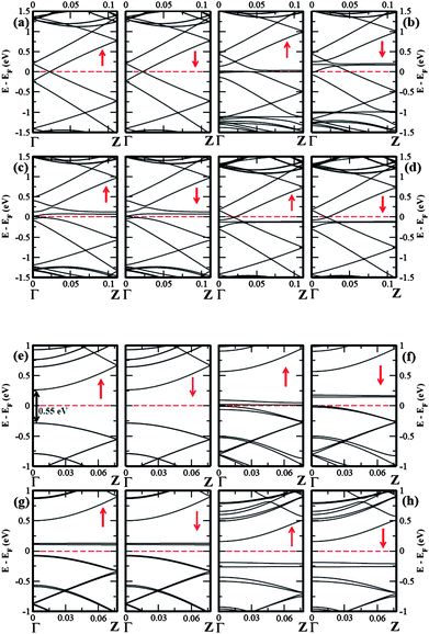 | ||
| Fig. 2 The spin-polarized electronic band structure for (a) pure (5,5) SWNT, (b) (5,5) SWNT@2TCNQ, (c) (5,5) SWNT@2TCNE, (d) (5,5) SWNT@2TTF, and (e) pure (8,0) SWNT, (f) (8,0) SWNT@2TCNQ, (g) (8,0) SWNT@2TCNE, (h) (8,0) SWNT@2TTF. The Fermi level is set to zero. The up and down arrows indicate the majority and minority spin channel, respectively. | ||
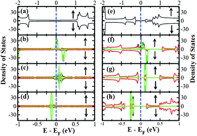 | ||
| Fig. 3 The spin-polarized total DOS and projected density of states (pDOS) for (a) pure (5,5) SWNT, (b) (5,5) SWNT@2TCNQ, (c) (5,5) SWNT@2TCNE, (d) (5,5) SWNT@2TTF, and (e) pure (8,0) SWNT, (f) (8,0) SWNT@2TCNQ, (g) (8,0) SWNT@2TCNE, (h) (8,0) SWNT@2TTF. The Fermi level is set to zero. The black, green and red color lines corresponds to the total DOS, molecule pDOS, and SWNT pDOS respectively. The up and down arrows indicate the majority and minority spin channel, respectively. The DOS lines are broadened with Gaussian functions of width 0.01 eV. | ||
For an understanding of the contribution of each constituent of the complexes to the low-energy characteristics, we have presented the spin-resolved projected density of states (pDOS) along with total DOS for all six SWNT-molecule complexes in Fig. 3. It is clear from the figure that the DOS near the Fermi level mainly originates from the adsorbed molecule which is the manifestation of SWNT-molecule interactions. In fact, the nanotube in SWNT-molecule complex contributes only significantly to the overall DOS at the Fermi energy giving rise to the metallic behavior for the TCNQ adsorbed on semiconducting (8,0) SWNT. Also, there is a finite spin-polarization at the Fermi energy as can be seen from the Fig. 3. Moreover, a net spin-polarization effect is also observed at the Fermi energy for the TCNQ adsorbed onto metallic (5,5) SWNT. It is also clear from Fig. 3 that at Fermi energy, a finite spin polarization only exists for TCNQ adsorbed on both types of nanotubes. Our findings are in reasonably good agreement with previous calculations31 and experimental results.29,28
To probe whether the molecular charge transfer of these physisorbed systems can affect the transport behavior of the modified 1D SWNTs, we consider calculating optical conductivity, a soft technique that can be obtained from reflectivity measurement, for pure SWNTs together with the various SWNT-molecule complexes. The optical conductivity is given by the Kubo formula,22,31 and the conductivity computed here does not include time dependent DFT or scissors corrections. The frequency (ω) dependent conductivity (σ(ω)) is calculated along the periodic nanotube axis of 1D SWNT (e.g. along z-axis) for all systems. We plot the low frequency regime of the optical conductivity for all the systems in Fig. 4. Note that, for pure 1D SWNTs, the Fermi level lies exactly in between the valence band and conduction band resulting in only the possibility of inter band electronic transitions. Also note that there are selection rules51 for band-to-band transitions and the intensity as well as the peak frequency depend strongly on the transition probability. For (3,3), (5,0) and (4,2) nanotubes, it was found that the optical conductivity peak appears above ∼2.9 eV, ∼1.2 eV and ∼1.9 eV, respectively.52 In our case, the optical conductivity peak appears only above ∼2.50 eV and ∼1.20 eV, respectively for (5,5) SWNT and (8,0) SWNT. However, for molecule adsorbed on SWNTs, the Fermi level shifts towards the valence band or conduction band relative to the pure case depending on the nature of the molecule, as mentioned earlier. This creates the possibility of Drude like intra-band transitions along with possibility of having transition to or from the strongly localized flat molecular levels, resulting in the low frequency optical excitation below the above mentioned values. This would also give evidence for physisorption with appearance of flat molecular levels in between the valence and conduction bands. Interestingly, the significant amount of charge transfer together with spin-polarization for TCNQ-adsorbed SWNTs reflects in the low-frequency optical conductivity profile. In fact, this induces asymmetry in the population of majority and minority spins at the Fermi level (see Fig. 2), which result in the difference in conductivity values for the carriers with different spins in the low frequency region (see Fig. 4). However, for TCNE- and TTF-adsorbed SWNTs, both the spin channels have symmetric population (see Fig. 2) together with comparatively lesser extent of charge transfer and thereby shows less intense low-frequency peaks. Moreover, the larger extent of charge transfer for (5,5) SWNT-molecule complexes induces greater carriers population at the Fermi level, and hence more intense peaks in the low-frequency conductivity profile in comparison to the semiconducting (8,0) SWNT-molecule complexes.
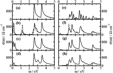 | ||
| Fig. 4 Low-frequency optical conductivity for pure (5,5) SWNT, (b) (5,5) SWNT@2TCNQ, (c) (5,5) SWNT@2TCNE, (d) (5,5) SWNT@2TTF, and (e) pure (8,0) SWNT, (f) (8,0) SWNT@2TCNQ, (g) (8,0) SWNT@2TCNE, (h) (8,0) SWNT@2TTF for incoming light polarized parallel to the nanotube axis. The solid and dashed lines in the conductivity profiles correspond to the majority and minority spins, respectively. The lines are broadened with Gaussian functions of width 0.05 eV. | ||
To verify the consistency of our results, we also consider a distinct metallic (9,0) SWNT which has different diameter and chirality from the previous one. Although the pure (9,0) SWNT has a pseudo gap exactly at the Fermi energy, after interaction with TCNE, it opens up the band gap supporting our findings as a general case. Furthermore, since the TCNQ, a strong electron acceptor, on interaction with semiconducting (8,0) SWNT closes up the gap as discussed earlier, we too have thought to consider a better and stronger electron-withdrawing adsorbate molecule, a fluorinated derivative of TCNQ i.e. tetrafluoro quinodimethane (F4-TCNQ), and find similar semiconductor-metal transition.
4. Conclusions
We have shown that the presence of organic donor and acceptor molecules on SWNTs surface can significantly change the electronic properties, using first-principles DFT-GGA method. For all cases, the magnitude of adsorption energies are found to be moderate, suggesting physisorption process. We find that the redistribution of charges occur in SWNTs as well as for adsorbed molecule induced by an effective fractional charge transfer between the two. We find a downward shift of Fermi level relative to that for the pristine SWNTs for TCNE and TCNQ adsorbed both type SWNTs, whereas the Fermi level shifts upward from that for TTF intercalated SWNTs. Interestingly, we find that the surface adsorption of selective organic donor–acceptor molecules on different SWNTs can give rise to the tuning of band gap with possibility of metal to semiconductor transition or vice versa depending on the nature of the adsorbed molecule. We also suggest that these effects can be seen in optical conductivity profiles as the low frequency regions are affected by the interactions with adsorbed molecules, providing a soft probe technique for identifying signatures of molecular charge-transfer interactions. Since adsorption of donor and acceptor molecules gives rise to tuning of band-gap as well as transition in electronic state, we conjecture that it is possible to fabricate the nanotube-based electronic devices through simple means, possibly through selective surface adsorption of both donor and acceptor molecules.Acknowledgements
We are grateful to Prof. C. N. R. Rao for inspirations and encouragement. AKM acknowledges CSIR, Govt of India for a research fellowship and SKP acknowledges CSIR and DST, Govt. of India.Notes and references
- G. Dresselhaus, M. S. Dresselhaus and P. C. Eklund, Science of Fullerenes and Carbon Nanotubes: Their Properties and Applications (Academic, New York, 1996) Search PubMed.
- K. S. Novoselov, A. K. Geim, S. V. Morozov, D. Jiang, Y. Zhang, S. V. Dubonos, I. V. Grigorieva and A. A. Firsov, Science, 2004, 306, 666 CrossRef CAS.
- Y. Zhang, Y.-W. Tan, H. L. Stormer and P. Kim, Nature, 2005, 438, 201 CrossRef CAS.
- C. Berger, Z. Song, X. Li, X. Wu, N. Brown, C. Naud, D. Mayou, T. Li, J. Hass, A. N. Marchenkov, E. H. Conrad, P. N. First and W. A. de Heer, Science, 2006, 312, 1191 CrossRef CAS.
- M. Y. Han, B. Ozyilmaz, Y. Zhang and P. Kim, Phys. Rev. Lett., 2007, 98, 206805 CrossRef.
- F. Schedin, A. K. Geim, S. V. Morozov, E. W. Hill, P. Blake, M. I. Katsnelson and K. S. Novoselov, Nat. Mater., 2007, 6, 652 CrossRef CAS.
- B. Huard, J. A. Sulpizio, N. Stander, K. Todd, B. Yang and D. Goldhaber-Gordon, Phys. Rev. Lett., 2007, 98, 236803 CrossRef CAS.
- R. H. Baughman and et al. , Science, 1999, 284, 1340 CrossRef CAS.
- J. Kong, N. R. Franklin, C. Zhou, M. G. Chapline, S. Peng, K. Cho and H. Dai, Science, 2000, 287, 622 CrossRef CAS.
- C. Staii and A. T. Johnson, Nano Lett., 2005, 5, 1774 CrossRef CAS.
- A. Star and et al. , Proc. Natl. Acad. Sci. U. S. A., 2006, 103, 921 CrossRef CAS.
- D. A. Heller and et al. , Science, 2006, 311, 508 CrossRef CAS.
- K. Keren, R. S. Berman, E. Buchstab, U. Sivan and E. Braun, Science, 2003, 302, 1380 CrossRef CAS.
- R. Martel, T. Schmidt, H. R. Shea, T. Hertel and Ph. Avouris, Appl. Phys. Lett., 1998, 73, 2447 CrossRef CAS.
- S. J. Wind, J. Appenzeller, R. Martel, V. Derycke and Ph. Avouris, Appl. Phys. Lett., 2002, 80, 3817 CrossRef CAS.
- W. Y. Kim, Y. C. Choi and K. S. Kim, J. Mater. Chem., 2008, 18, 4510 RSC.
- W. Y. Kim and K. S. Kim, J. Comput. Chem., 2008, 29, 1073 CrossRef CAS.
- S. S. Mallajosyula, P. Parida and S. K. Pati, J. Mater. Chem., 2009, 19, 1761 RSC.
- W. Y. Kim and K. S. Kim, Nat. Nanotechnol., 2008, 3, 408 CrossRef CAS.
- S. S. Mallajosyula and S. K. Pati, J. Phys. Chem. B, 2008, 112, 16982 CrossRef CAS.
- S. Dutta, S. Lakshmi and S. K. Pati, Phys. Rev. B: Condens. Matter Mater. Phys., 2008, 77, 073412 CrossRef.
- S. S. Mallajosyula and S. K. Pati, J. Phys. Chem. B, 2007, 111, 13877 CrossRef CAS.
- S. Dutta and S. K. Pati, J. Phys. Chem. B, 2008, 112, 1333 CrossRef CAS.
- S. Dutta, A. K. Manna and S. K. Pati, Phys. Rev. Lett., 2009, 102, 096601 CrossRef.
- B. Huang, Y.-W. Son, G. Kim, W. Duan and J. Ihm, J. Am. Chem. Soc., 2009 Search PubMed.
- A. Das, S. Pisana, B. Chakraborty, S. Piscanec, S. K. Saha, U. V. Waghmare, K. S. Novoselov, H. R. Krishnamurthy, A. K. Geim, A. C. Ferrari and A. K. Sood, Nat. Nanotechnol., 2008, 3, 210 CrossRef CAS.
- B. Das, R. Voggu, C. S. Rout and C. N. R. Rao, Chem. Commun., 2008, 5155 RSC.
- R. Voggu, C. S. Rout, A. D. Franklin, T. S. Fisher and C. N. R. Rao, J. Phys. Chem. C, 2008, 112, 13053 CrossRef CAS.
- N. Varghese, A. Ghosh, R. Voggu, S. Ghosh and C. N. R. Rao, J. Phys. Chem. C, 2009, 113, 16855 CrossRef CAS; C. N. R. Rao, A. K. Sood, K. S. Subrahmanyam and A. Govindaraj, Angew. Chem., Int. Ed., 2009, 48, 7752 CrossRef CAS.
- R. Voggu, B. Das, C. S. Rout and C. N. R. Rao, J. Phys.: Condens. Matter, 2008, 20, 472204 CrossRef.
- A. K. Manna and S. K. Pati, Chem.–Asian J., 2009, 4, 855 CrossRef CAS.
- M. Kalbac, L. Kavan, L. Dunsch and M. S. Dresselhaus, Nano Lett., 2008, 8, 1257 CrossRef CAS.
- M. A. Pimenta, G. Dresselhaus, M. S. Dresselhaus, L. G. Cancado, A. Jorio and R. Saito, Phys. Chem. Chem. Phys., 2007, 9, 1276 RSC.
- L. Duclaux, Carbon, 2002, 40, 1751 CrossRef CAS.
- J. E. Fischer, Acc. Chem. Res., 2002, 35, 1079 CrossRef CAS.
- R. Voggu, S. Paul, S. K. Pati and C. N. R. Rao, J. Phys.: Condens. Matter, 2008, 20, 215211 CrossRef.
- R. Saito, G. Dresselhaus and M. S. Dresselhaus, Physical Properties of Carbon Nanotubes, Imperial College Press, London, UK, 1998 Search PubMed.
- C. N. R. Rao and A. Govindaraj, Nanotubes and Nanowires, RSC Nanoscience & Nanotechnology Series, RSC Publishing, Cambridge, UK, 2005 Search PubMed.
- J. Lu, S. Nagase, X. Zhang, D. Wang, M. Ni, Y. Maeda, T. Wakahara, T. Nakahodo, T. Tsuchiya, T. Akasaka, Z. Gao, D. Yu, H. Ye, W. N. Mei and Y. Zhou, J. Am. Chem. Soc., 2006, 128, 5114 CrossRef CAS.
- A. Das, A. K. Sood, A. Govindaraj, M. Saitta, M. Lazzeri, F. Mauri and C. N. R. Rao, Phys. Rev. Lett., 2007, 99, 136803 CrossRef.
- H. J. Shin, S. M. Kim, S. M. Yoon, A. Benayad, K. K. Kim, S. J. Kim, H. Ki Park, J. Y. Choi and Y. H. Lee, J. Am. Chem. Soc., 2008, 130, 2062 CrossRef CAS.
- C. N. R. Rao, A. K. Sood, R. Voggu and K. S. Subrahmanyam, J. Phys. Chem. Lett., 2010, 1(2), 572 Search PubMed.
- A. Das, A. K. Sood, P. K. Maiti, M. Das, R. Varadarajan and C. N. R. Rao, Chem. Phys. Lett., 2008, 453, 266 CrossRef CAS.
- J. M. Soler, E. Artacho, J. D. Gale, A. Garcia, J. Junquera, P. Ordejon and D. Sanchez-Portal, J. Phys.: Condens. Matter, 2002, 14, 2745 CrossRef CAS; P. Ordejon, E. Artacho and J. M. Soler, Phys. Rev. B: Condens. Matter, 1996, 53, R10441–R10444 CrossRef CAS.
- K. Burke, J. P. Perdew and M. Ernzerhof, Int. J. Quantum Chem., 1997, 61, 287 CrossRef CAS.
- N. Troullier and J. L. Martins, Phys. Rev. B: Condens. Matter, 1991, 43, 1993 CrossRef CAS.
- L. Kleinman and D. M. Bylander, Phys. Rev. Lett., 1982, 48, 1425 CrossRef CAS.
- F. Ortmann, W. G. Schmidt and F. Bechstedt, Phys. Rev. Lett., 2005, 95, 186101 CrossRef CAS.
- D. R. Salahub, Adv. Chem. Phys., 1987, 69, 447 CAS.
- D. Wegner, R. Yamachika, Y. Wang, V. W. Brar, B. M. Bartlett, J. R. Long and M. F. Crommie, Nano Lett., 2008, 8, 131 CrossRef CAS.
- S. Reich, C. Thomsen, and J. Maultzsch, Carbon Nanotubes, Basic Concepts and Physical Properties (Wiley-VCH, Berlin, 2004) Search PubMed.
- M. Machon, S. Reich, C. Thomsen, D. Sanchez-Portal and P. Ordejon, Phys. Rev. B: Condens. Matter Mater. Phys., 2002, 66, 155410 CrossRef.
| This journal is © The Royal Society of Chemistry 2010 |