Numerical investigations into mechanical properties of hexagonal silicon carbon nanowires and nanotubes
Bin
Zheng
* and
John E.
Lowther
School of Physics and DST/NRF Centre of Excellence in Strong Materials, University of the Witwatersrand, Johannesburg, South Africa. E-mail: bin.zheng@wits.ac.za
First published on 7th July 2010
Abstract
Single-crystalline hexagonal faceted silicon carbon nanowires and nanotubes possess simultaneous high strength and failure strain. As long as SiC nanowires or nanotubes are large or thick enough to sustain a single atomic configuration under loading, their mechanical properties are size independent. Surface atoms are firstly forced to move by stretching and then destroy the equilibrium of subsurface atoms. Then, the force in carbon–silicon bonds along the tensile directions becomes larger than that in other bonds and results in elongation by three-times of the former than that of the latter. However, the latter bonds connecting the surface to the subsurface are broken and the wires or tubes are ruptured. For thinner nanowires and nanotubes, the broken bonds don't propagate instantly, but initiate transformation from a wurtzite to a graphitic structure. This structure transformation can strengthen and plasticize SiC nanowires and nanotubes.
1. Introduction
When the characteristic scale of materials shrinks below 100 nm, the elastic moduli of many materials show a pronounced increase and deformation defects nucleate with increasing difficultly.1,2 Consequently, ultrahigh strength has been observed in several nanomaterials, including ceramics nanostructures,3 graphene monolayers,4 germanium,5 glass silica nanowires,6 carbon nanotubes,7,8 and metal/graphite core/shell nanoparticles.2 However, these high strength materials usually show small strain to their first yield even though they possess super-ductility in later deformation.9,10 For widely used semiconductor materials, the first yield is very important and may bring destructive fracture. Efforts to improve it are usually found to be at the expense of strength, and the reason for this is not at all clear.11 There is therefore a limit on the applications of such materials in nanoscale devices, which demand continuous adjustable strength over a large range of deformation. Thus, the quest for materials integrating good strength with high first-failure strain has become a common goal to both scientists and engineers. Due to its excellent mechanical properties, silicon carbon (SiC) as a nanostructured material has been suggested to be a good candidate.12,13The analysis focuses on the mechanical deformation of SiC nanowires (NWs) and nanotubes (NTs), which are particularly attractive for device applications. They have been created experimentally through a catalyst-free method,14 chemical vapor deposition process,15 the reaction of silicon with multi-wall carbon NT16,17 and a reduction–carburization route by using SiCl4, CCl4 or C6Cl6.18,19 Among these experimental products, the cubic 3C structure (SiC crystalline possesses more than 150 polytypes) is usually observed, two factors should be considered. First, their amorphous coating can reduce the number of dangling bonds and then stabilise the cubic structure.20,21 Second, characterization measurements (such as electron beam in TEM) may facilitate the structure transformation into a cubic structure.17 Based on this, most theoretical research aims at low-dimension SiC nanostructures employing a cubic structure, in spite of possible changes in structure due to their small size.13,22
Some researchers have proposed that nanostructures of 3C-SiC are stabilised in the size range of beyond 20 nm, whereas SiC nanostructure only stabilises a 2H structure at a small range below 20 nm.23,24 Zou et al.25 have prepared 2H-SiC nanostructure with a key size of ∼15 nm through a one-step solvothermal route, as suggested for above theoretical results. Furthermore, the electrical and optical properties of wurtzite SiC nanostructure, such as their narrow and indirect-band gaps, are attracting more attention.24 Although 3C-SiC possesses a diamond structure, the 2H bulk structure may have higher strength.26 These results indicate that 2H-SiC nanostructure is an important semiconductor structure with great potential application in nanoscale devices, such as sensors, transducers, and actuators in nanoelectromechanical systems (NEMS). In this work, we performed a theoretical evaluation on the mechanical deformation of hexagonal structure SiC nanowires and nanotubes by means of molecular dynamics (MD) simulation.
2. Simulation methodology
We have considered SiC NWs and NTs that were built with 2H-SiC (hexagonal) single-crystalline structure, the unit cell of which was shown in Fig. 1(a). Faceted SiC NWs were simulated by cutting a solid wire out of the bulk 2H-SiC crystal with a hexagonal cross section and faceted SiC NTs were then created by removing atoms from the centre of the solid wires leaving a hexagonal hole and forming thick wall tubes. The morphology of these NWs and NTs was characterized as hexagonal prisms with [0001]-oriented axis enclosed by six facets belonging to the {100} plane group of 2H-SiC crystal, as shown in Fig. 1(b). The SiC NWs were indexed by the number of hexagon units between two opposite angles in the hexagonal cross section (5NW in Fig. 1c), while the faceted NTs were indexed by adding the number of hexagon units in the hexagonal hole cross section (9hollow7 NT in Fig. 1d). For each hexagon unit, the distance between two opposite sides is 3.073 Å, which is consistent with the lattice parameter a of 2H-SiC crystal.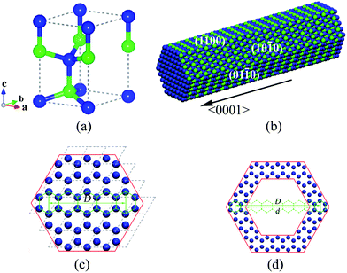 | ||
| Fig. 1 Different views of single-crystalline 2H-SiC nanowires and nanotubes with hexagonal faceted morphology: (a) the unit cell of the bulk SiC; (b) a representation of faceted nanowires; (c) top view of 5NWs, the dash lines are for showing unit cell; (d) top views of 9Hollow7 NTs. The blue balls represent Si atoms, and the green ones are C atoms. The definitions of the diameter (D and d) are shown in (c) and (d) and their unit is the number of hexagon unit. | ||
All numerical simulations reported here are performed using an analytical bond-order potential for SiC, the successful validation of which for configurations ranging from the molecular to the bulk regime indicates the transferability of this potential model and makes it a good choice for atomistic simulations that sample a large configuration space.27
To obtain detailed analyses on the relationship between the structural deformation and mechanical properties of SiC nanostructures as well as the influence of defects and their size, we employed MD simulation to perform uniaxial tensile loading under simulated quasistatic conditions.9,28 MD simulation was carried using the LAMMPS software29,30 with time steps of 1 fs. Energy-minimization, which is based on the conjugate gradient (CG) algorithm and guarantees an atomic optimization position, was performed first. Then, internal stresses were released by relaxing the nanostructure under constant atmosphere pressure (NPT) for 1 ns and under constant volume (NVT) for another 1 ns to thermally equilibrate the system at 300 K using a Nosé–Hoover thermostat.31,32 Tensile deformation was performed along the axial direction with periodic boundary conditions in a stepwise manner, rather than continuously. For each step, the nanowires or nanotubes were first displaced according to a prescribed uniform displacement increment of 1 Å in the length direction. The wires and tubes were then relaxed at constant temperature for 500 ps to obtain a macroscopic equilibrium configuration at the prescribed displacement. These stretching–equilibration iterations gave an equivalent 0.2 m s−1 (0.002% ps−1) stretch rate and were repeated for many times until the rupture of wires or tubes. Even the stretching rate reduced to 0.02 m s−1 (0.0002% ps−1), we found no significant difference in their stress–strain relationships and atomic mechanisms of mechanical deformation. The stresses reported in this work were calculated via summing all atoms' stress tensor along tensile direction and then being divided by the volume of the system.
3. Results and discussion
Stress–strain curves for all SiC nanowires and nanotubes materials loaded in tension are shown in Fig. 2. From this Figure we note some characteristics of interest. One is their ultrahigh strength values (> ∼90 GPa), which are comparable to values reported in literature for carbon nanotubes.7,8 Our values are larger than that evaluated by ab initio, because the DFT calculation employed a periodic boundary for bulk SiC on one hand, and the Tersoff potential overestimated the strength value on the other.26 In addition, the first yielding strains reach to 24% for those large wires and tubes. Third, the ultimate tensile stresses and the final rupture strains of 9NW, 7NW and 5NW are almost the same; however, thinner 3NW possesses higher strength and better deformability (Fig. 2a). Fourth, stretching results of 2H-SiC nanotubes with different wall thickness show that their mechanical properties depend on the wall thickness, i.e. thinner tubes, higher fracture stress and strain (Fig. 2c).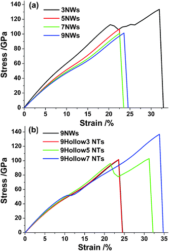 | ||
| Fig. 2 Stress–strain relationships in the case of (a) different size of 2H faceted SiC nanowires; (b) different thickness of 2H faceted SiC nanotubes. | ||
The calculated and experimental Young's modulus of SiC NWs and NTs are summarized in Table 1. From this Table, our results for 2H-SiC NWs are well within the range of the experimental data (230–750 GPa) for large diameter of NWs (35–286 nm) from ref. 33, but they are higher than calculated values of 3C-SiC NWs with almost the same size. On the other hand, comparison between the Young's modulus of faceted NTs and single-wall NTs depends on the definition of thickness (δR) of single-wall NTs. We took δR = 0.33 nm and then our calculated Young's modulus of faceted NTs is higher than that of single-wall NTs.
| SiC NWs | SiC NTs | ||||||
|---|---|---|---|---|---|---|---|
| 2H | 3C | Faceted NTs | Single-wall cylindrical NTs | ||||
| D/nm | Young modulus/GPa | D/nm | Young modulus/GPa | [(D0 − DI)/2]/nm | Young modulus/GPa | D 0/nm | Young modulus/GPa |
| a Ref. 22. b Ref. 13. c Ref. 34. d Ref. 36. e Ref. 37. f Ref. 33. g Ref. 38. h Ref. 39. | |||||||
| 0.91 | 679 | 0.69 | 635a | 0.36 (D0 = 1.48) | 670 | 0.7 | 472.7g |
| 0.99 | 622a, 504.8b | ||||||
| 1.48 | 601 | 1.32 | 613a | 0.36(D0 = 2.15) | 598 | 0.97 | 539.4g, 487.9h |
| 1.65 | 525.2b, 520c | ||||||
| 2.15 | 562 | 1.98 | 532c, 520d | 0.36 (D0 = 2.62) | 572 | 1.392 | 548.5h |
| 2.31 | 537.4b | ||||||
| 2.62 | 547 | 2.64 | 546c | 0.59 (D0 = 2.62) | 560 | 1.995 | 554.5h |
| 21.5 | 660e | ||||||
| 3.2 | 538 | 23.0 35-286 | 610e230–750f | 0.89 (D0 = 2.62) | 550 | ||
Furthermore, the calculated Young's modulus (E) of 2H-SiC nanowires decrease with increasing size. Consider the fitting error in linear regression, the modulus are almost the same in larger size of nanowires (>2.15 nm). For β-SiC nanowires, reported results represent opposite trends of Young's modulus with increasing diameter: decreasing modulus in the diameter range from 0.69 to 1.32 nm22 and increasing modulus at large range 1.65–2.64 nm.34 More results indicated that the size dependence of Young's modulus of β-SiC nanowires was not clear at large sizes.13,33 Liang et al.35 thought that size-dependent elasticity of nanowires was contributed by two factors: surface modulus and core nonlinear elasticity. The latter is due to surface stress inducing size-dependent strains which are well beyond the linear elastic regime. And for some materials, their stress–strain response quickly becomes non-Hookean for strains in excess of small strain, such as 1%. We calculated the stress–strain curves of 2H-SiC bulk and found that they obey Hook law even strain >3%, which was used to obtain Young's modulus of SiC nanowires via linear regression. Makeev et al.13 found that the quadratic behavior occurs when the tensile strain is larger than 10% in 3C-SiC. Thus, the surface modulus becomes the dominant effect that determines the elasticity of SiC nanowires. Consider the ratio of surface atoms to total atoms in SiC nanowires, we found that in the diameter range from 0.91 to 2.15 nm the difference of the surface–total atoms ratio under different diameter was larger than that in the diameter range >2.15 nm, and then its effect on elasticity of nanowires is obvious in small size.
The nanowire surface is always softer than the (equivalent) bulk due to the surface atoms decreasing in their coordination, but the softening from surface atoms does not always increase with decreasing diameter. In <110> orientation Cu nanowires, the surface softening decreased in small size.35 Our simulation shows that the Young's modulus of 2H-SiC nanowires decreased with increasing diameter, as is consistent with the trend from Yan et al. in the diameter range from 0.69 to 1.32 nm.22 For the size-dependent surface modulus, this trend can be contributed to distribution of electron density across the surface layers of nanowires or nanotubes on one hand, and geometric factor of hexagonal cross sections of nanowires or nanotubes on the other hand. More detailed work for explaining this size effect will be performed by ab initio calculations and shown in later reports.
The ideal strength for a perfect defect-free material can be evaluated to be on the order of ∼E/2π or ∼E/π.5,6 Thus, our Young's modulus values bring the theoretical strength. Fig. 2 shows that the ultimate strength of SiC nanowires and nanotubes reaches their ideal strength. However, the measured tensile strengths in experiment will be always lower than theoretical predictions for perfect nanowires or nanotubes, two factors should be considered: the presence of small twist or shear loads or both in experimental loading method; and the structure defects existing in the outer shell.
Besides their ultrahigh strength, a large deformation for achieving idea strength is also interesting. In order to identify deformation mechanisms behind these various observations, the tensile behavior was analysed by examining the statistics of Si–C–Si (or C–Si–C) bonds angle distribution, as shown in Fig. 3 (b). Note that we considered those bond angles (dark region in Fig. 3a) built by bond 1 (along tensile direction) and bond 2 (any other direction). At the original state of SiC NWs, bond angle distribution exhibits a sharp peak at ∼109° due to the perfect tetrahedral arrangements of atoms. On loading, the distribution peak shifted toward high angle. Further loading resulted in one small peak emerging on the right of the main peak. At a strain of ∼18%, the two peaks united as one broadened peak. With further stretching, the broad peak gradually became sharp and then realized the second shift of the main peak of bond angle distribution.
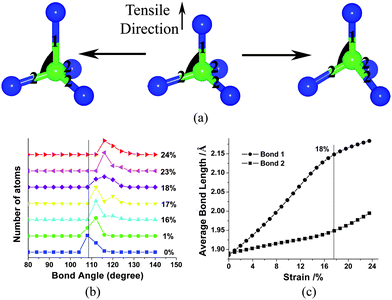 | ||
| Fig. 3 The variation of bond angle and bond length under tensile loading: (a) a schematic diagram of changing bond angle (dark region) and bond length in tetrahedron configuration; (b) the bond angle distribution of 7NW at different tensile strain, these curves have been shifted to show the variation of bond angle distribution clearly; (c) the bond length variation with the increasing strain, bond 1 represents C–Si bonds along the tensile direction, and bond 2 is the C–Si bonds along other direction. | ||
Variation of the bond angle shown in Fig. 3(b) results from the relative displacement of its atom component. Due to the uniaxial loading, the atomic displacement mainly referred to the movement along the tensile direction. The almost invariant section area in stretching also indicated the negligible atomic lateral displacement. Further, we examined the atomic coordinate of the tetrahedral unit in every tensile step and found that apex and centre atoms always move upwards relative to bottom atoms, as shown in Fig. 3(a). In this Figure, we fixed bottom atoms and considered two types of ideal motion: one is that the apex atom moves and the centre atom is fixed (the left in Fig. 3a); another is that centre atom moves and the relative distance between the apex atom and centre atom keep invariant (the right in Fig. 3a). The observed atomic motion is a complex of above two types of ideal movement. Fig. 3(a) shows that variation of bond angle is due to the vertical movement of the centre atom, irrespective of the displacement of apex atoms.
Actually, the above two types of relative motion correspond to length variation of Si–C bond 1 and bond 2, respectively. We examined the variation of Si–C bonds length in the uniaxial tensile process of a wire, as shown in Fig. 3(c). Both of the two types of bond keep their length continuous rising. Length increasing of bond 1 is faster than that of bond 2, especially at the strain range of low ∼18%. This fact results in the total elongation of bond 1 is about three times larger than that of bond 2 and then it becomes the main contributor to the large deformation capacity of SiC NWs. We also found that ∼18% strain point separates from the different increasing rates of bond length, i.e. the length of bond 1 increases from fast to slow and that of bond 2 rises with an opposite rule. These differences between bond 1 and bond 2 can be attributed to the fact that stretching of bond 1 in Fig. 3(a) won't change the bond angles and then becomes easier than that of bond 2. Increasing the length of bond 2 accumulates slowly to a certain extent and then can trigger right-shifting of the bond angle distribution in Fig. 3(b).
Different behaviors between bond 1 and bond 2 can be understood by analysing the force equilibrium in the tensile direction, as given in Fig. 4. In the Figure, the chain is stretched vertically. The relationship between N, F1, F2 and F3 can be obtained by considering force equilibrium of centre atoms in the vertical direction: N = F1·cosα1 + F2·cosα2 + F3·cosα3. It can be seen that the magnitude of F1, F2 or F3 is equal to N for those inner atoms of NWs at the original state (α1 = α2 = α3 = ∼71°). In this indicative model, bottom atoms are fixed. At the start of the tensile loading, surface atoms (“A” and “B” in Fig. 4) are unbalanced in force owing to their dangling bonds and they are forced to move up by stretching first, and then bond angle α2 increases. Thus, the equilibrium of subsurface centre atom (“C” in Fig. 4) is broken (N > F1·cosα1 + F2·cosα2 + F3·cosα3) and it moves up to obtain a new equilibrium state. Subsequently, bond angles α1, α2 and α3 decrease and the magnitude of F1, F2 or F3 in bond 2 becomes lower than N in bond 1 in new equilibrium state. The different magnitude of force in bond 1 and bond 2 in the stretching process takes main responsibility to their different contributions to deformability.
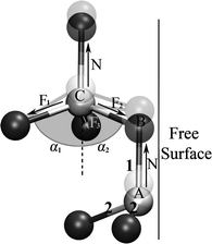 | ||
| Fig. 4 Mechanism of atomic bond breakage by analysing the geometry of bond force acting at surface atoms and then subsurface atoms. The black spheres represent atoms located at the angles of a tetrahedron, and the white spheres are the centre atoms of a tetrahedron. The force carried by the chain in bond 1 is denoted by N while F1, F2 and F3 denote the force in bond 2 in every tetrahedron. α denotes the included angle between C–Si bonds and the tensile direction. Shade denotes those surface atoms after moving along tensile direction. | ||
Although the elongation of bond 1 is large, bond 2 is broken down first. This can be understood by analysing the equilibrium of bond 2 (“B–C” in Fig. 4) connecting the surface to subsurface of NWs, which is the first unbalanced site of NWs in every tensile step. When loading is small, it is possible for the unstable state to relax to a new equilibrium state owing to loose interatomic space. Once loading reaches the top value, the atomic bond looks like a tight rubber band and any imbalance will bring destructive fracture. The first destruction is those bonds connecting the surface to the subsurface of NWs. Fig. 5(a) shows that the bonds 2 close to the free surface are broken first. Rapidly, the breakage propagates towards the inner NWs (Fig. 5b). Once the cracks from the free surface meet and connect in the inner wires, bonds 1 breakage is triggered (Fig. 5c) and SiC NWs rupture instantly (Fig. 5d).
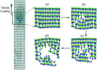 | ||
| Fig. 5 Fracture of 7NWs under tensile loading: (a) beginning, dark lines denote those facture bonds; (b) propagating; (c) and (d) rupture. | ||
We note some stress drop points in stress–strain curves of 2H nanowires with excellent deformability (Fig. 2). In order to identify the mechanisms behind these discrete stress points, the detailed tensile deformation of thinner 2H nanowires is given in Fig. 6 for a limited length. The original wurtzite crystals in the wire experienced homogeneous longitudinal stretching without significant structure transformation up to 19.4% strain (Fig. 6a and b). Only with further stretching did a substantial number of C–Si bonds break between the surface and subsurface of NW. This is confirmed by the sharp drop of the stress at stress–strain curve in Fig. 2(a). As time elapses, more C–Si bonds broke and a separation of surface atoms and inner atoms appeared. As a result, the hexagonal section of wire gradually transformed into a circle shape (Fig. 6c, d and e).
 | ||
| Fig. 6 The atomic structure evolution of 3NW at strain levels of (a) 0%, (b) 19.4%, (c) 20.3%, (d) 30.1%, and (e) 31.9%. | ||
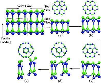
From the above observations, the 3NW didn't rupture instantly, although a number of C–Si bonds were broken down. The bond breakage in small SiC wire plays a role in inducing a new structure, i.e. a layered tube. Zhang et al. calculated the cohesive energy of 3C-SiC NWs and SiC single-wall NTs as a function of diameter and found that NTs were more stable than their NWs counterparts below a critical diameter ranging from 1.4 to 1.7 nm.39 Furthermore, the calculation of formation energy between faceted 2H-SiC NWs and layered NTs also showed that the latter were more stable than the former with similar diameters.24 Mechanical loading can assist in crossing the energy barrier between the two structures and the transformation was initiated and propagated via breaking C–Si bonds connecting atomic layers in our simulation. It is interesting that a similar structure transformation under mechanical loading was observed in SiC nanotubes with thinner walls (Fig. 7).
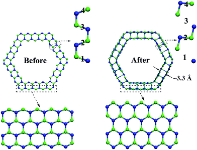 | ||
| Fig. 7 Atomic structure of 9Hollow7 NTs before and after structure transformation. The numbers “1”, “2”, “3” and “4” denote those bonds connecting the outmost layer with the sublayer. | ||
Prior to the structure-transformation of tubes, the connection between surface atoms and subsurface atoms was through tightly arranged C–Si bonds, and as a result was significantly strong. In every layer the hexagonal network consists of alternating Si in a single plane and C atoms displaced below this plane with each Si atom having as nearest neighbors only C atoms and vice versa. This type of SiC graphene structure was more stable. Single-wall SiC nanotubes by rolling up the graphene structure exhibited excellent mechanical, electronic and transport properties.40,41 But, the wave like or “rippled” features of this structure, consisting not entirely of planar atoms in every layer of the tube, resulted in a large number of C–Si bond connections between tube layers.
The structure transformation of our tubes under loading was accompanied with rotation and breakage of bonds connecting the surface layer to the adjacent layer. The sharp drop of the stress in the stress–strain curve in Fig. 2(b) can confirm the structure transformation, which is driven more easily in thinner tubes. The tube radius can affect the cross-sectional shape of final layered NTs, such as 5Hollow3 nanotubes, in which atomic structure is transformed from faceted NTs to cylindrical layered SiC NTs, not hexagonal layered NTs in large tubes. For new structures, the rotating C–Si bonds (“2” and “4” in Fig. 7) alternate with the fractured bonds (“1” and “3” in Fig. 7) along the tensile direction. The breakage bonds facilitated the relaxation of those non-coplanar atoms, while the rotating bonds still maintained tight coupling between layers and then the interwall connection was superior to van der Waals force connections.8,42 The interlayer spacings of the layered nanotubes were ∼3.3 Å, which is similar in value to the multiwalled carbon nanotube (3.4 Å). This also holds for the result that strength of SiC nanotube is comparable to that of carbon nanotube in Fig. 2. However, the spacings in many cases were found to be as large as 4.5 Å, and some researchers considered that no real multiwalled layered SiC nanotubes exist owing to their very loose coupling between layers.41 Our results represent layered SiC nanotubes, which are induced from thin facted nanotubes by mechanical loading.
In terms of geometry, these layered tubes can be considered as a rolled-up relaxed SiC graphene sheet. Thus, our 2H-SiC NWs and NTs actually undergo a transformation from a wurtzite to a graphitic structure under mechanical loading. A similar structure transformation has been predicted in ZnO nanostructures.43
We used the analytical formulation in ref. 43 to discuss our structure transformation. In this simulation, all nanowires and nanotubes diameters are finite and changed. Thus, we can give the energy difference (ΔE) between graphitic and wurtzite structure for a total of N SiC bonds in a nanowire or nanotube as:
| ΔE = [(EG2 − EG1)(nG/N) − (EW2 − EW1)(nW/N)] + (EG1 − EW1) | (1) |
From eqn (1), we know that the critical condition for wurtzite–graphitic structure transformation is defined as ΔE = 0 and the first term is negative but the second term is positive. It is noted that all energy values in this equation are independent of size. Thus, the ratio of missing bonds to total bonds (n/N), which always decreases with reduced diameters in fixed length of wires and tubes no mater the structure, is only one adjustable variant. Once n/N is large enough (in thinner nanowire or nanotube), the graphitic SiC structure which is unstable in the bulk can become stable in nanoscale size, especially under the assistance of mechanical loading. The critical diameter of 2H-SiC wires is 1 nm and the critical thickness of 2H faceted tubes is 0.6 nm, when their length is 96 nm in this work. Therefore, our simulation shows that the structure transformation in 2H-SiC nanowires and nanotubes is a direct result of surface of reconstruction and additional mechanical loading will assist the transformation.
4. Conclusions
In summary, we utilized a molecular dynamics method to perform uniaxial tensile deformation of single-crystalline hexagonal SiC nanowires and nanotubes. As long as they are large or thick enough to sustain a single atomic configuration under loading, their strength and deformability are independent of the wire/tube radius. These nanowires and nanotubes yield first at a strain of 24% and rupture at their maximum theoretical strength. The C–Si bonds along the tensile direction stretched three times more than other bonds, and takes main responsibility for stretching deformability. Once loading reaches yield force, C–Si bonds connecting surface to subsurface were firstly broken and the breakage rapidly spread into the interior, and finally resulted in rupture of wires or tubes. The structure transformation from faceted nanowires/nanotubes to layered structures was observed in small nanowires or thin wall nanotubes under tensile loading. These were due to surface reconstruction and initiated through breaking Si–C bonds connecting the outer layer to the inner adjacent layer and promoted the strength and the failure-strain further. Thus, these nanowires or nanotubes materials are expected to be valuable building blocks in the development of future nanoscale devices.Acknowledgements
We acknowledge support from the DST/NRF Centre of Excellence in Strong Materials, South Africa.Notes and references
- G. Stan, C. V. Ciobanu, P. M. Parthangal and R. F. Cook, Nano Lett., 2007, 7, 3691–3697 CrossRef CAS.
- S. Suresh and J. Li, Nature, 2008, 456, 716–717 CrossRef CAS.
- I. Szlufarska, A. Nakano and P. Vashishta, Science, 2005, 309, 911–914 CrossRef CAS.
- C. Lee, X. Wei, J. W. Kysar and J. Hone, Science, 2008, 321, 385–388 CrossRef CAS.
- L. T. Ngo, D. Almécija, J. E. Sader, B. Daly, N. Petkov, J. D. Holmes, D. Erts and J. J. Boland, Nano Lett., 2006, 6, 2964–2968 CrossRef CAS.
- G. Brambilla and D. N. Payne, Nano Lett., 2009, 9, 831–835 CrossRef CAS.
- M. F. Yu, B. S. Files, S. Arepalli and R. S. Ruoff, Phys. Rev. Lett., 2000, 84, 5552–5555 CrossRef CAS.
- M. F. Yu, O. Lourie, M. J. Dyer, K. Moloni, T. F. Kelly and R. S. Ruoff, Science, 2000, 287, 637–640 CrossRef CAS.
- L. Dai, W. C. D. Cheong, C. H. Sow, C. T. Lim and V. B. C. Tan, Langmuir, 2010, 26, 1165–1171 CrossRef CAS.
- F. Ma, S. L. Ma, K. W. Xu and P. K. Chu, Nanotechnology, 2009, 20, 045601 CrossRef CAS.
- Z. W. Shan, G. Adesso, A. Cabot, M. P. Sherburne, S. A. Syed Asif, O. L. Warren, D. C. Chrzan, A. M. Minor and A. P. Alivisatos, Nat. Mater., 2008, 7, 947–952 CrossRef CAS.
- X. D. Han, Y. F. Zhang, K. Zheng, X. N. Zhang, Z. Zhang, Y. J. Hao, X. Y. Guo, J. Yuan and Z. L. Wang, Nano Lett., 2007, 7, 452–457 CrossRef CAS.
- M. A. Makeev, D. Srivastava and M. Menon, Phys. Rev. B: Condens. Matter Mater. Phys., 2006, 74, 165303 CrossRef.
- G. Z. Yang, H. Cui, Y. Sun, L. Gong, J. Chen, D. Jiang and C. X. Wang, J. Phys. Chem. C, 2009, 113, 15969–15973 CrossRef CAS.
- J. Wei, Phys. E., 2009, 41, 1810–1813 CrossRef CAS.
- Z. Pan, H. L. Lai, F. C. K. Au, X. Duan, W. Zhou, W. Shi, N. Wang, C. S. Lee, N. B. Wong, S. T. Lee and S. Xie, Adv. Mater., 2000, 12, 1186–1190 CrossRef CAS.
- X. H. Sun, C. P. Li, W. K. Wong, N. B. Wong, C. S. Lee, S. T. Lee and B. K. Teo, J. Am. Chem. Soc., 2002, 124, 14464–14471 CrossRef CAS.
- J. Q. Hu, Q. Y. Lu, K. B. Tang, B. Deng, R. R. Jiang, Y. T. Qian, W. C. Yu, G. E. Zhou, X. M. Liu and J. X. Wu, J. Phys. Chem. B, 2000, 104, 5251–5254 CrossRef CAS.
- G. Shen, D. Chen, K. Tang, Y. Qian and S. Zhang, Chem. Phys. Lett., 2003, 375, 177–184 CrossRef CAS.
- H. F. Zhang, C. M. Wang and L. S. Wang, Nano Lett., 2002, 2, 941–944 CrossRef CAS.
- C. H. Liang, G. W. Meng, L. D. Zhang, Y. C. Wu and Z. Cui, Chem. Phys. Lett., 2000, 329, 323–328 CrossRef CAS.
- B. Yan, G. Zhou, W. Duan, J. Wu and B. L. Gu, Appl. Phys. Lett., 2006, 89, 023104 CrossRef.
- T. Ito, K. Sano, T. Akiyama and K. Nakamura, Thin Solid Films, 2006, 508, 243–246 CrossRef CAS.
- Z. Wang, M. Zhao, T. He, X. Zhang, Z. Xi, S. Yan, X. Liu and Y. Xia, J. Phys. Chem. C, 2009, 113, 856–861 CrossRef CAS.
- G. Zou, C. Dong, K. Xiong, H. Li, C. Jiang and Y. Qian, Appl. Phys. Lett., 2006, 88, 071913 CrossRef.
- Y. Umeno, Y. Kinoshita and T. Kitamura, Modell. Simul. Mater. Sci. Eng., 2007, 15, 27–37 CrossRef CAS.
- P. Erhart and K. Albe, Phys. Rev. B: Condens. Matter Mater. Phys., 2005, 71, 035211 CrossRef.
- L. Dai, C. H. Sow, C. T. Lim, W. C. D. Cheong and V. B. C. Tan, Nano Lett., 2009, 9, 576–582 CrossRef CAS.
- S. Plimpton, J. Comput. Phys., 1995, 117, 1–19 CrossRef CAS.
- http://lammps.sandia.gov/index.html ( 2009).
- S. Nosé, J. Chem. Phys., 1984, 81, 511–519 CrossRef CAS.
- W. G. Hoover, Phys. Rev. A: At., Mol., Opt. Phys., 1985, 31, 1695–1697 CrossRef.
- S. Perisanu, V. Gouttenoire, P. Vincent, A. Ayari, M. Choueib, M. Bechelany, D. Cornu and S. T. Purcell, Phys. Rev. B: Condens. Matter Mater. Phys., 2008, 77, 165434 CrossRef.
- Z. Wang, X. Zu, F. Gao and W. J. Weber, Phys. Rev. B: Condens. Matter Mater. Phys., 2008, 77, 224113 CrossRef.
- H. Liang, M. Upmanyu and H. Huang, Phys. Rev. B: Condens. Matter Mater. Phys., 2005, 71, 241403 CrossRef.
- Z. Wang, X. Zu, Z. Li and F. Gao, J. Phys. D: Appl. Phys., 2008, 41, 155419 CrossRef.
- E. W. Wong, P. E. Sheehan and C. M. Lieber, Science, 1997, 277, 1971 CrossRef CAS.
- B. Baumeier, P. Krüger and J. Pollmann, Phys. Rev. B: Condens. Matter Mater. Phys., 2007, 76, 085407 CrossRef.
- Y. Zhang and H. Huang, Comput. Mater. Sci., 2008, 43, 664–669 CrossRef CAS.
- H. Shen, Comput. Mater. Sci., 2009, 47, 220–224 CrossRef CAS.
- M. Menon, E. Richter, A. Mavrandonakis, G. Froudakis and A. N. Andriotis, Phys. Rev. B: Condens. Matter Mater. Phys., 2004, 69, 115322 CrossRef.
- S. Okada, S. Saito and A. Oshiyama, Phys. Rev. B: Condens. Matter Mater. Phys., 2002, 65, 165410 CrossRef.
- L. Zhang and H. Huang, Appl. Phys. Lett., 2007, 90, 023115 CrossRef.
| This journal is © The Royal Society of Chemistry 2010 |