Tuning the shape and thermoelectric property of PbTe nanocrystals by bismuth doping
Qian
Zhang
a,
Ting
Sun
b,
Feng
Cao
c,
Ming
Li
d,
Minghui
Hong
ef,
Jikang
Yuan
c,
Qingyu
Yan
b,
Huey Hoon
Hng
b,
Nianqiang
Wu
d and
Xiaogang
Liu
*a
aDepartment of Chemistry, National University of Singapore, Singapore, 117543. E-mail: chmlx@nus.edu.sg; Fax: +65-65161791
bDepartment of Materials Science and Engineering, Nanyang Technological University, Singapore, 639798
cDepartment of Applied Physics, The Hong Kong Polytechnic University, Kowloon, Hong Kong SAR, China
dDepartment of Mechanical and Aerospace Engineering, West Virginia University, Morganton, USA 26506
eDepartment of Electrical and Computer Engineering, National University of Singapore, Singapore, 117543
fOptical Materials and Systems Division, Data Storage Institute, A*STAR, Singapore, 117608
First published on 19th May 2010
Abstract
We report the synthesis of a series of monodispersed Bi-doped PbTe nanocrystals with tunable morphologies by using a doping precursor of bismuth(III) 2-ethylhexanoate. The as-synthesized Pb1−xBixTe (x = 0.005, 0.010, 0.015, 0.020) nanocrystals are characterized by X-ray diffraction, X-ray photoelectron spectroscopy and Hall measurements. The nanocrystals with controlled spherical, cuboctahedral, and cubic shapes were readily prepared by varying the Bi doping concentration. Thermoelectric investigation of these nanocrystals shows that the Bi3+ doping increases electrical conductivity from 350 to 650 K and changes the Seebeck coefficient sign from positive to negative.
Introduction
Thermoelectric (TE) materials can directly convert thermal energy into electrical energy upon applying a thermal gradient to the materials. These materials are playing an increasingly important part in a diverse range of applications as heat pumps and electrical power generators.1–4 The efficiency of TE materials can be measured by the material's dimensionless figure of merit ZT (ZT = α2σT/κ, where α is the Seebeck coefficient or thermopower, T is the absolute temperature, and σ and κ are the electrical conductivity and thermal conductivity). The thermal conductivity comprises contribution from electrons and phonons.5Maximizing ZT is often achieved by minimizing the thermal conductivity by promoting interface-phonon scattering. It has been proposed that nanostructured materials can enhance ZT due to the occurrence of the quantum confinement effect, which increases thermopower α resulting from an increased local density of states near the Fermi level.6–8 Despite recent development in nanocrystal synthesis,9–17 it has been challenging to prepare small-sized thermoelectric nanocrystals with controlled doping composition and concentration.18–20 For instance, although bismuth (Bi) has been used as an n-type dopant in PbTe thin films and bulk materials for thermoelectric studies,21,22 the preparation of well-defined Bi-doped PbTe nanoparticles with controlled doping levels remains a substantial challenge.
In this study, we show that it is plausible to synthesize monodispersed Bi-doped PbTe nanocrystals with controlled sizes and morphologies by utilizing bismuth(III) 2-ethylhexanoate as the Bi precursor. Importantly, we show that the Bi doping results in electrical conductivity enhancement in the PbTe nanocrystals, providing promising uses for thermoelectric applications.
Experimental
In a typical synthesis, 1 mmol of lead acetate trihydrate (> 99%) and stoichiometric amounts of bismuth(III) 2-ethylhexanoate were dissolved in 5 ml of 1-octadecene and 1 ml of oleic acid (both technical grade, 90%) in a 50 ml flask. The resulting mixture was heated at 90 °C under stirring for three hours to form a light yellow solution. A stock solution (0.75 M) of tellurium was separately prepared by adding the tellurium powder (99.8%) into trioctylphosphine (≥ 97%) with vigorous stirring overnight. Subsequently, a 4 ml tellurium stock solution was quickly injected into the solution of lead acetate at a temperature of 150 °C. After two minutes, the flask was cooled in an ice bath to precipitate the nanocrystals. The as-formed nanocrystals were washed with absolute ethanol several times, further precipitated by centrifugation, and re-dispersed with cyclohexane. All syntheses were performed in an argon atmosphere using a Schlenk line.X-Ray power diffraction (XRD) analysis was carried out on a Siemens D5005 X-ray diffractometer with Cu Kα radiation (λ = 1.5406 Å). The particle morphology and selected area electron diffraction (SAED) were examined by transmission electron microscopy (TEM, JEOL 2010) operating at an acceleration voltage of 200 kV. X-Ray photoelectron spectra (XPS) were performed with a PHI 5000 Versa Probe system (Physical Electronics, MN) using a monochromatic Al Kα X-ray source (1486.6 eV). The pass energy of the hemisphere analyzer was maintained at 117.4 eV for survey scan and 58.7 eV for high-resolution scan, while the takeoff angle was fixed at 45°. Binding energies of XPS spectra were corrected by referencing the C1s signal of adventitious hydrocarbon to 284.8 eV. XPS data fittings were carried out with PHI multipakTM software using the Gauss-Lorenz mode and Shirley background. For preparation of nanoparticle films, the as-synthesized nanoparticles were washed with N2H4·H2O and ethanol (v/v; 1![[thin space (1/6-em)]](https://www.rsc.org/images/entities/char_2009.gif) :4) to remove capping surfactants and re-dispersed in ethanol prior to spray-coating onto a glass substrate and subsequently annealing under H2/Ar at 350 °C for 30 min. The electrical properties of the films were measured by a ZEM-3 Seebeck meter from 350 to 650 K. The thickness of the film was obtained by using a surface profile scanning system (α-step IQ). The surface morphology of the films was investigated by field-emission scanning electron microcopy (SEM, JEOL6710). The Hall measurements were conducted on a Lake Shore 7600 Hall measurement system from 300 K to 100 K.
:4) to remove capping surfactants and re-dispersed in ethanol prior to spray-coating onto a glass substrate and subsequently annealing under H2/Ar at 350 °C for 30 min. The electrical properties of the films were measured by a ZEM-3 Seebeck meter from 350 to 650 K. The thickness of the film was obtained by using a surface profile scanning system (α-step IQ). The surface morphology of the films was investigated by field-emission scanning electron microcopy (SEM, JEOL6710). The Hall measurements were conducted on a Lake Shore 7600 Hall measurement system from 300 K to 100 K.
Results and discussion
The crystal structures of the as-synthesized Bi-doped PbTe (Pb1−xBixTe; x = 0, 0.005, 0.010, 0.015 and 0.020) samples were first examined by XRD and the results are shown in Fig. 1. All diffraction peaks can be indexed to face-centered cubic (fcc) rock-salt structures with a space group of Fm3m (JCPDS: 78-1904). The slight peak shifts towards higher diffraction angles in the X-ray powder diffraction patterns as a function of the Bi3+ ion concentration, can be attributed to the contraction in unit-cell volume due to the substitution of Pb2+ ions by smaller Bi3+ ions in the host lattice. The lattice parameter was found to decrease with an increase in the dopant concentration (Fig. 1, inset). The solubility limit of bismuth in PbTe was estimated to be x = 0.015.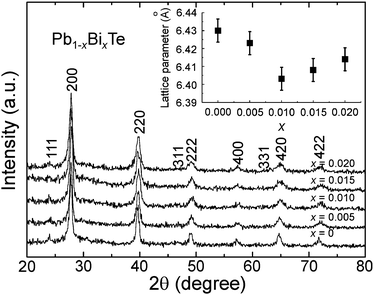 | ||
| Fig. 1 XRD patterns of the as-synthesized Pb1−xBixTe (x = 0, 0.005, 0.010, 0.015 and 0.020) samples (inset: the lattice parameter of the samples as a function of Bi3+ doping concentration x). | ||
It has been reported that lead chalcogenide nanoparticles with controlled feature size and morphology can be obtained by varying the reaction time, surfactant concentration, and ratio of metal precursors.23,24 We found that the doping of Bi3+ at different doping levels through use of bismuth(III) 2-ethylhexanoate as the doping precursor resulted in the formation of PbTe nanoparticles with tunable particle size (10–15 nm) and morphology. To exclude the possibility of reaction time effect on the nanocrystal growth, all the reactions were carried out for two minutes and immediately quenched by pouring the reaction mixtures into an ice bath. The effect of Bi3+ doping on the morphology of the nanocrystals was presented in Fig. 2. With no Bi3+ added, monodispersed spherical PbTe nanoparticles were obtained with an average particle size of 10 nm.25 On doping of Bi3+ with increased concentrations (x = 0.005, 0.010, 0.015), the nanocrystal morphology changes from spherical shape to cuboctahedral and cubic shapes. Notably, the doping of Bi3+ also leads to an increase in the nanocrystal size.
 | ||
| Fig. 2 (a), (c), (e) and (g) Corresponding TEM images of the as-synthesized Pb1−xBixTe nanocrystals at x = 0, 0.005, 0.010 and 0.015, respectively. (b) SAED pattern obtained for samples shown in Fig. 2(a), indicating cubic PbTe structures. (d), (f) and (h) Corresponding HRTEM images of the nanocrystals shown in (c), (e) and (g), respectively. The scale bars are 50 nm for (a), (c), (e) and (g) and are 5 nm for (d), (f) and (h). | ||
The shape evolution of the PbTe nanocrystals as a function of Bi3+ dopant can be attributed to the relative growth rates on different crystallographic planes.26,27 In the rock-salt crystal structure, the {111} plane generally has a higher surface energy than the {100} plane.23 On increasing reaction time, the {111} facets grow faster than the {100} facets, resulting in the formation of cubic-shaped nanocrystals dominated with {100} planes. For example, it was reported that the spherical/cuboctahedral-to-cubic shape conversion for pure PbTe nanocrystals requires more than 20 min of reaction time.24 In contrast, our doping approach results in the shape conversion within 2 min. The effect on shortening the reaction time can be ascribed to the addition of 2-ethylhexanoate, which stabilizes the {100} facets and promotes the relative growth rate of the {111} facets.
To verify the crystal composition and the presence of stabilizing molecules bound to the crystal surface, the PbTe nanocrystals doped with 1 mol% Bi3+ were examined by XPS as shown in Fig. 3. Fig. 3(a) shows the XPS spectrum that provides a survey scan of the nanocrystals. All peaks can be assigned to Pb, Te, Bi, O and C. The Pb4f7/2 and Pb4f5/2 peaks were observed at 137.2 and 142.3 eV respectively, which were the characteristic values for PbTe (Fig. 3(b)). The high-binding-energy shoulder peaks at 138.4 and 143.2 eV correspond to the expected chemical shifts for either Pb(OH)2 or PbO (Fig. 3(b)).28 The Te3d5/2 and Te3d3/2 peaks were observed at 571.9 and 582.3 eV, which were diagnostic of PbTe (Fig. 3(c)). Two groups of peaks at 575.8 and 586.2 eV were assigned to TeO2 (Fig. 3(c)).28 The two sub-bands of Bi4f at 158 (Bi4f5/2) and 163.4 eV (Bi4f7/2) further confirm the presence of Bi3+ dopant in PbTe nanocrystals.29 The high-binding-energy shoulder peaks at 159 and 164.4 eV were assigned to Bi2O3 (Fig. 3(d)). The C1s and O1s peaks at 284.8 and 530 eV were attributed to oleic acid or 2-ethylhexanoate molecules bound to the particle surface (Fig. 3(e) and (f)).
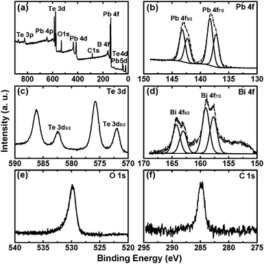 | ||
| Fig. 3 (a) XPS survey scan of the as-synthesized Pb0.99Bi0.01Te nanoparticles. (b)–(f) High-resolution XPS spectra of respective Pb4f, Te3d, Bi4f, O1s and C1s regions of the Pb0.99Bi0.01Te nanoparticles. | ||
To evaluate the TE application of the Bi-doped nanoparticles, the nanoparticle thin films doped with varied amounts of Bi were prepared by an air brush spray system. The hydrazine treatment was employed to remove the organic ligands for increased electrical contact of the nanoparticle systems.30 The surface morphology of an as-prepared film after annealing at 350 °C is shown in Fig. 4(a). Upon annealing, the nanoparticles were enlarged to 20–30 nm. The quantum confinement effect is expected as the average size of the enlarged nanoparticles is still smaller than the Bohr exciton radius (∼46 nm) of PbTe.31 The electrical resistance and the Seebeck coefficient of the samples were measured from 350 to 650 K and plotted as a function of temperature in Fig. 4(b) and (c), respectively. In contrast to the PbTe nanoparticle film without the Bi3+ dopant, the films made from Bi-doped PbTe nanocrystals showed marked decreases of electrical resistance (Fig. 4(b)) and negative Seebeck coefficients (Fig. 4(c)). The negative Seebeck coefficients, which are consistent with the results obtained by the Hall measurements shown in Fig. 4(d), provide another proof of the successful doping of the Bi3+ into the PbTe nanocrystals. The Bi-doped PbTe nanocrystals doped with 1.5 mol% Bi3+ exhibited a high Seebeck coefficient of −325 μV K−1 at 350 K, which is consistent with the theoretical value (−350 μV K−1) for n-type PbTe structures that possess the same electron carrier concentration.31
 | ||
| Fig. 4 (a) A representative SEM image of the film made from Bi-doped PbTe nanoparticles. The scale bar is 1 μm. Inset is a high magnification SEM of the film shown in Fig. 4(a) and the scale bar is 100 nm. (b) Temperature dependence studies of the electrical resistance for the films made from Pb1−xBixTe (x = 0, 0.005, 0.010, 0.015, 0.020) nanoparticles. Inset is an enlarged area of electrical resistance measured between 450 and 650 K. (c) Corresponding Seebeck coefficient measurements obtained from the films made from Bi-doped PbTe nanoparticles (inset: the Seebeck coefficient measurement of the film made from undoped PbTe nanoparticles). (d) Corresponding Hall coefficient measurements obtained from the films made from Bi-doped and undoped PbTe nanoparticles. | ||
The Hall mobility of films made from Bi-doped PbTe nanocrystals (1 mol% Bi3+) was derived by using μH = RH/ρ, (where μH, RH, and ρ refer to the Hall mobility, Hall coefficient and the electrical resistance, respectively) and plotted as a function of logT from 300 to 100 K (Fig. 5, left panel). The Hall mobility of the Bi-doped film (∼0.6 cm2 V−1 s−1) at 300 K is lower than that of the undoped film (∼2.1 cm2 V−1 s−1), which is attributed to the inverse relationship between carrier concentration and Hall mobility. In the right panel of Fig. 5, the log μHvs. logT graph was presented, giving rise to the power exponent δ (μ ≈ T−δ) of ∼1.9 at 100–200 K and ∼3.5 at 200–300 K with the logμH curve deviating from a straight line at ∼200 K. The results, which are also found in Pb0.99La0.01Te bulk materials, are consistent with the behavior of the weakly or intermediate degenerate n-type PbTe semiconductors.32
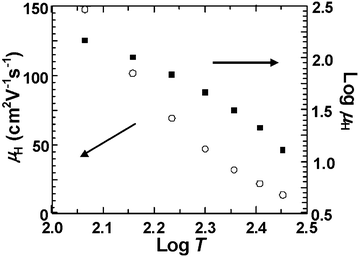 | ||
| Fig. 5 μ H (left panel) and logμH (right panel) as a function of logT for the Pb0.99Bi0.01Te nanoparticle film. | ||
Conclusions
We have developed a new method for the synthesis of single-crystalline Bi-doped PbTe nanocrystals by using bismuth(III) 2-ethylhexanoate as the Bi3+ precursor. The incorporation of the Bi3+ dopant at different doping levels in the nanocrystal host lattice was confirmed by XRD, XPS, and Hall measurements. Importantly, we have demonstrated that the doping approach imparts a substantial impact on the growth process to give dual control over the size and shape of the resulting nanocrystals. Investigation of the thermoelectric properties of films made from these nanocrystals shows decreased electrical resistance from 350 to 650 K as compared to undoped nanocrystal films.Acknowledgements
This work was supported in part by the National University of Singapore (NUS) Academic Research Fund, the Singapore-MIT Alliance, and the Agency for Science, Technology and Research (A*STAR). X. L. is grateful to the NUS for a Young Investigator Award. We thank L. Tian and J. Xu for technical assistance.Notes and references
- B. C. Sales, Science, 2002, 295, 1248 CrossRef CAS.
- F. Zhou, J. Szczech, M. T. Pettes, A. L. Moore, S. Jin and L. Shi, Nano Lett., 2007, 7, 1649 CrossRef CAS.
- W. Zhou, J. Zhu, D. Li, H. H. Hng, F. Y. C. Boey, J. Ma, H. Zhang and Q. Yan, Adv. Mater., 2009, 21, 3196 CrossRef CAS.
- T. M. Tritt, Science, 1996, 272, 1276 CAS.
- Thermoelectrics Handbook: Macro to Nano, ed. D. M. Rowe, Taylor & Francis, New York, 2006 Search PubMed.
- M. S. Dresselhaus, G. Chen, M. Y. Tang, R. Yang, H. Lee, D. Wang, Z. Ren, J. Fleurial and P. Gogna, Adv. Mater., 2007, 19, 1043 CrossRef CAS.
- J. P. Heremans, V. Jovovic, E. S. Toberer, A. Saramat, K. Kurosaki, A. Charoenphakdee, S. Yamanaka and G. J. Snyder, Science, 2008, 321, 554 CrossRef CAS.
- B. Poudel, Q. Hao, Y. Ma, Y. Lan, A. Minnich, B. Yu, X. Yan, D. Wang, A. Muto, D. Vashaee, X. Chen, J. Liu, M. S. Dresselhaus, G. Chen and Z. Ren, Science, 2008, 320, 634 CrossRef CAS.
- Y. Wu, C. Wadia, W. Ma, B. Sadtler and A. P. Alivisatos, Nano Lett., 2008, 8, 2551 CrossRef CAS.
- M. Oh and C. A. Mirkin, Nature, 2005, 438, 651 CrossRef CAS.
- X. Liu, Angew. Chem., Int. Ed., 2009, 48, 3018 CrossRef CAS.
- R. S. Selinsky, D. J. Keavney, M. J. Bierman and S. Jin, Appl. Phys. Lett., 2009, 95, 202501 CrossRef.
- Q. Yan, H. Chen, W. Zhou, H. H. Hng, F. Y. C. Boey and J. Ma, Chem. Mater., 2008, 20, 6298 CrossRef CAS.
- F. Wang, Y. Han, C. S. Lim, Y. Lu, J. Wang, J. Xu, H. Chen, C. Zhang, M. Hong and X. Liu, Nature, 2010, 463, 1061 CrossRef CAS.
- F. Wang and X. Liu, Chem. Soc. Rev., 2009, 38, 976 RSC.
- L. Cademartiri, J. Bertolotti, R. Sapienza, D. S. Wiersma, G. Von Freymann and G. A. Ozin, J. Phys. Chem. B, 2006, 110, 671 CrossRef CAS.
- F. Wang, X. Xue and X. Liu, Angew. Chem., Int. Ed., 2008, 47, 906 CrossRef CAS.
- G. M. Dalpian and J. R. Chelikowsky, Phys. Rev. Lett., 2006, 96, 226802 CrossRef.
- S. C. Erwin, L. Zu, M. I. Haftel, A. L. Efros, T. A. Kennedy and D. J. Norris, Nature, 2005, 436, 91 CrossRef CAS.
- T. Ji, W. Jian and J. Fang, J. Am. Chem. Soc., 2003, 125, 8448 CrossRef CAS.
- T. C. Harman, M. P. Walsh, B. E. Laforge and G. W. Turner, J. Electron. Mater., 2005, 34, L19 CrossRef CAS.
- Y. Chen, T. J. Zhu, S. H. Yang, C. Yu and X. B. Zhao, J. Phys. D: Appl. Phys., 2010, 43, 035405 CrossRef.
- S. M. Lee, S. N. Cho and J. Cheon, Adv. Mater., 2003, 15, 441 CrossRef CAS.
- W. Lu, J. Fang, K. L. Stokes and J. Lin, J. Am. Chem. Soc., 2004, 126, 11798 CrossRef CAS.
- J. E. Murphy, M. C. Beard, A. G. Norman, S. P. Ahrenkiel, J. C. Johnson, P. Yu, O. I. Micic, R. J. Ellingson and A. J. Nozik, J. Am. Chem. Soc., 2006, 128, 3241 CrossRef CAS.
- Z. L. Wang, J. Phys. Chem. B, 2000, 104, 1153 CrossRef CAS.
- X. Liu, N. Wu, B. H. Wunsch, R. J. Barsotti Jr. and F. Stellacci, Small, 2006, 2, 1046 CrossRef CAS.
- Y. Yang, S. C. Kung, D. K. Taggart, C. Xiang, F. Yang, M. A. Brown, A. G. Guell, T. J. Kruse, J. C. Hemminger and R. M. Penner, Nano Lett., 2008, 8, 2447 CrossRef CAS.
- E. J. Menke, M. A. Brown, Q. Li, J. C. Hemminger and R. M. Penner, Langmuir, 2006, 22, 10564 CrossRef CAS.
- D. V. Talapin and C. B. Murray, Science, 2005, 310, 86–90 CrossRef CAS.
- T. J. Zhu, X. Chen, Y. Q. Cao and X. B. Zhao, J. Phys. Chem. C, 2009, 113, 8085 CrossRef CAS.
- K. Ahn, C. P. Li, C. Uher and M. G. Kanatzidis, Chem. Mater., 2009, 21, 1361 CrossRef CAS.
| This journal is © The Royal Society of Chemistry 2010 |