Metal nanowire grating patterns
G. U.
Kulkarni
* and
B.
Radha
Chemistry and Physics of Materials Unit and DST Unit on Nanoscience, Jawaharlal Nehru Centre for Advanced Scientific Research, Jakkur P.O., Bangalore, 560064, India. E-mail: kulkarni@jncasr.ac.in; Fax: +91-80-2208 2766; Tel: +91-80-2208 2814
First published on 8th June 2010
Abstract
Metal nanowire patterning in the form of grating structures has been carried out using a wide range of lithography techniques, and many hybrid methods derived from them. The challenge is to achieve sub-100 nm linewidths with controllable spacing and thickness over large areas of substrates with high throughput. In particular, the patterns with linewidth and spacing of a few tens of nm offer properties of great interest in optoelectronics and plasmonics. Crossbar grating structures—two gratings patterned perpendicular to each other—will play an important role as ultra-high density electrode grids in memristive devices for non-volatile memory.
 G. U. Kulkarni G. U. Kulkarni | G. U. Kulkarni received his PhD in Solid State Chemistry (1992) from the Indian Institute of Science, Bangalore. He is currently a Professor at the Chemistry and Physics of Materials Unit, Jawaharlal Nehru Centre for Advanced Scientific Research. His main research interests are direct-write nanolithography, self assembly, optical and electronic properties of nanomaterials and molecular crystals. He has published over 160 research articles and coauthored a book on Nanocrystals. |
 B. Radha B. Radha | B. Radha obtained her MSc in chemistry (2007) from Sri Krishnadevaraya University. She is presently working towards her PhD degree under the supervision of Professor G. U. Kulkarni at the Chemistry and Physics of Materials Unit, Jawaharlal Nehru Centre for Advanced Scientific Research. Her work pertains to patterned synthesis of functional nanomaterials and molecular electronic devices. |
1. Introduction
Metal nanowires have attracted a great deal of interest during the last decade because of their unique electronic, optical, catalytic and other properties.1,2 These are essentially one dimensional objects, with lengths extending typically from tens of nm (nanometres) to a few μm (micrometres), sometimes called anisotropic nanoparticles.3 The nanowires’ properties crucially depend on their diameter or cross section. While extremely thin nanowires exhibit quantized conductance,4 nanowires with diameters comparable to or above the mean free path of the conducting electrons are expected to behave almost as their bulk counterparts. Their confinement in 1D also makes the surface plasmon absorption band of the nanowire to split into longitudinal and transverse components corresponding to light absorption and scattering along the long and the short axes, respectively. The longitudinal plasmon absorption band is tunable depending on the aspect ratio from visible to near-IR (infrared).3,5 The electric field is enhanced at the sharp tip of the nanowire, a property which is exploited in field emission, from metallic6 as well as in inorganic nanowires.7 In such instances, it is desirable to have the nanowires grown vertically to the substrate.8 There have been few reports on vertically grown metal nanowires.9–13,14 They find applications in gas sensing,15 catalysis,16 microbatteries17 and device integration.18 On the other hand, there have been a large number of reports on metal nanowires grown in plane and parallel to the substrate. In this case, the preferred arrangement is the nanowire grating pattern. The interplay between the 1D confinement in individual nanowires and the inter-wire coupling in the grating opens up new avenues in optoelectronics. Nanowires in grating patterns are produced generally through lithography processes than by conventional synthetic routes used for ‘free’ nanowires.This mini-review presents a comprehensive coverage of the literature on metal nanowire patterning with special focus on grating patterns, also termed as metal nanowire grating patterns (MNGPs). The essential set of parameters that define an MNGP are the nanowire linewidth, the periodic spacing (also called pitch) and the thickness (vertical to the substrate). Other descriptors include the metal, substrate, surface roughness as well as the linearity or curvature of the grating. The spacing is usually larger than the linewidth, and the thickness, much less than both. Here, we restrict the discussion to MNGPs with sub-100-nm linewidths, addressing the special properties borne out of confinement. We first present important fabrication methods and then move on to applications in devices.
2. Fabrication of MNGPs
There have been a number of conventional as well as innovative lithography processes to achieve sub-100-nm linewidths in metal nanowire patterning, which is pictorially presented in Fig. 1. They are classified under scanning probe and focused beam based techniques, optolithography, nanoimprint and soft lithography. Many hybrid methods are also shown. It has become customary that any new or a hybrid technique is usually first applied to produce an MNGP before trying out complex patterning, much like a beginning toddler! The full forms of the various acronyms are listed in Table 1.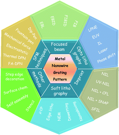 | ||
| Fig. 1 A palette displaying fabrication techniques used for MNGPs. | ||
| Acronym | Expansion |
|---|---|
| MNGP | Metal nanowire grating pattern |
| DPN | Dip-pen nanolithography |
| FA-DPN | Field assisted dip-pen nanolithography |
| EBL | Electron beam lithography |
| EBID | Electron beam induced deposition |
| FIB | Focussed ion beam |
| FIBID | Focussed ion beam induced deposition |
| LPNE | Lithographically patterned nanowire electrodeposition |
| EUV | Extreme ultraviolet |
| IL | Interference lithography |
| EUV-IL | Extreme ultraviolet interference lithography |
| NIL | Nanoimprint lithography |
| UV-NIL | Ultraviolet nanoimprint lithography |
| CFL | Capillary force lithography |
| SFIL | Step and flash imprint lithography |
| NEM | Nanoentrapment molding |
| μCP | Micro-contact printing |
| SNAP | Superlattice nanowire pattern transfer |
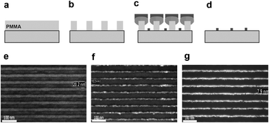
An immediately conceivable process is cutting parallel nanogrooves using a atomic force microscopy (AFM) tip on a sacrificial layer to deposit the metal of choice on top. Using a gentle force of 1 μN on the tip, Chen et al.19 scratched a poly(methylmethacrylate) (PMMA) film coated on an Si substrate to create a nanogroove array. In the following steps, e-beam evaporation of metal was performed and lift-off was carried out by sonicating the sample in acetone leaving behind an array of metal nanowires as shown in Fig. 2. The method was employed for a variety of metals, and linewidths down to 50 nm were routinely obtained. The ploughed polymer decorating the groove edges sets a lower limit on achievable spacing. A bilayer consisting of a thin Ti layer on top of PMMA seems to improve the resolution and ensures long-life of the tip without wearing and bending.20 Nanogroove patterning becomes facile under an electrical bias applied to the conducting AFM tip, which is known as ‘electrostatic nanolithography’.21 In this process, the AFM tip in proximity produces intense electric fields (∼109 V m−1) causing local ablation of the polymer. Thus-created nanogrooves are filled with metals.22 Instead of a polymer film, a metal-based resist may be used to be oxidized locally. Molybdenum is well suited for this purpose as Mo and MoO3 have high etch selectivity (MoO3 is soluble in water!). Using a sacrificial layer of PMMA in between the substrate and Mo film, Rolandi et al.23 produced a grating of MoO3 which was subsequently dissolved away in water during developing. The exposed polymer was removed by reactive ion etching (RIE). The nanotrenches were subsequently filled with Ti and developed to produce Ti-MNGP with linewidths down to ∼30 nm.
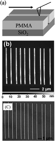 | ||
| Fig. 2 (a) Schematic showing nanoscratching of PMMA by an AFM tip. (b) AFM image of the grooves in the polymer. (c) SEM image of Au nanowires formed by depositing metal into the grooves and lift-off of PMMA in acetone (from ref. 19). | ||
Use of an AFM tip as delivery system or simply like a nib of a pen is popular in the form of ‘dip-pen nanolithography’ (DPN).24,25 The method exploits the water meniscus formed between a slowly scanning AFM tip and a substrate to transfer the species loaded on the tip to the substrate by diffusion.26 DPN has been used to write fine lines of etch resists on smooth metal films such as alkanethiols on Au, and following etching, line patterns of width ∼30 nm have been obtained.27,28 In order to have a more sustained supply of the ‘ink’, one may resort to fountain pen lithography.29 In this method, the ‘ink’ is fed from a reservoir through a microfluidic channel along the cantilever to the shell surrounding the tip. Other variants of DPN30 deliver the ink guided by an external stimulus such as electrical field applied to the tip, also called field assisted DPN (FA-DPN). It has been used to generate MNGPs of Fe of width ∼120 nm.31 These techniques have minimal dependence on humidity. The ink delivery can be virtually turned on or off without having to move the tip away from the substrate.
Conventional electron beam lithography (EBL) is routinely employed to write fine metal patterns. Working with a focused electron beam on a high resolution resists such as PMMA, hydrogen silsesquioxane, calixarene etc., line patterns of sub-20 nm width are commonly produced.32,33 A conducting substrate is clearly a prerequisite. However e-beam patterning of metal nanowires on insulating substrates such as glass has been achieved in presence of water vapor,34,35 which avoids charging effects during pattern exposure. Instead of using pure polymeric resists, metal–organic precursors such as alkanethiolates have proven advantageous for fabricating Pd- and Au-MNGPs.36,37 Here, the alkyl hydrocarbon serves as a highly sensitive resist by crosslinking and hosting defects internally. The metal can be liberated easily from the hydrocarbons following thermolysis after development. This is evidently a direct-write process, as demonstrated in Fig. 3.37 An interesting aspect of this method is that the inherent resistance of the metal nanowires can be controlled by adjusting the thermolysis temperature (see Fig. 3b). A direct write process using a liquid phase metal precursor is another potential technique for MNGPs.38 A focused electron beam has also been used to deposit MNGPs from vapor phase precursors by the well known process of electron beam induced deposition (EBID).39 Focussed ion beams (FIB) can also be used for depositing and milling of metal nanowires.40 For example, Au- and Pt-MNGPs down to 60 nm width have been accomplished using a 30 keV Ga+ ions.41 FIB also allows the fabrication of high resolution stencils for direct deposition of metal by physical means.42
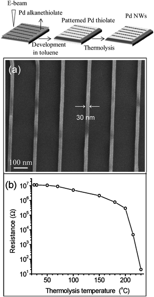 | ||
| Fig. 3 (Top) Schematic of the procedure adopted: step 1, spincoating of the Pd hexadecylthiolate on a Si surface, EBL patterning; step 2, developing the patterned substrate in toluene and; step 3, thermolysis of Pd thiolate nanowires at 250 °C to give Pd nanowies. (a) SEM images showing thermolyzed Pd nanowires, (b) semilog plot of resistance versus thermolysis temperature (from ref. 37). | ||
Optolithography has proven versatile for patterning of metal and other nanostructures over the last two decades. Unlike EBL and AFM based techniques, this is not a serial process and hence offers high throughput. However, one of the serious shortcomings of the optical based methods is that their resolution is limited due to edge diffraction. Innovative methods have been developed in recent years, ‘cheating’ the diffraction limit.43 In the process known as lithographically patterned nanowire electrodeposition (LPNE),44,45 the sacrificial metal (Ni) is over-etched to create nanogrooves under a polymeric resist roof, to bring in another metal of choice (Au, Ag, Pd, Pt) by electrodeposition. After the photoresist lift-off, Ni is selectively etched to leave behind the desired MNGP. Here, the sacrificial electrode, Ni, delimits one edge of the nascent nanowire, whereas the photoresist ‘ceiling’ constrains its height during growth. The width of the nanowire is determined by the electrochemical deposition parameters. The process is illustrated in Fig. 4. Minimum linewidths of 11 nm and heights of 5 nm have been obtained.44,45
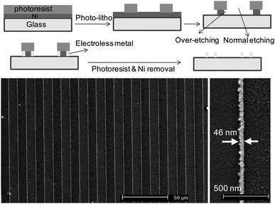 | ||
| Fig. 4 (Top) Process flow for metal-nanowire fabrication using LPNE. Below is shown Au-MNGP (1 cm in length and spaced by 9 μm). A magnified view of a Pt nanowire of width 46 nm from the same process is on the bottom right (from ref. 44). | ||
Employing optical beams with shorter wavelengths is one way to address the diffraction limited resolution.46 However owing to increased absorption at short wavelengths, operation in vacuum and use of special materials for masks and focusing optics becomes necessary.47 An easy way round for MNGPs is to use maskless lithographic techniques48 such as interference lithography.49 Typically, light from a synchrotron radiation source in the wavelength range of 5–50 nm is made to undergo interference to produce a set of parallel light beams of nanometric width. In combination with modified approaches to metal deposition such as deposition at oblique angles (shadow masking), this process can deliver sub-100 nm MNGPs. One such process from Auzelyte et al.50 is illustrated in Fig. 5. Using visible wavelength for conventional patterning, but exploiting the side walls of a patterned polymeric resist, Ag fin structures with 60 nm wall thickness have been produced.51 Laser-induced chemical vapor deposition of metals has been effectively used to produce MNGPs both by direct writing using a focused beam or using interference patterns from a broad beam. Importantly, this calls for a suitable metal–organic precursor which readily undergoes decomposition when exposed to the laser beam. One such study made use of W(CO)6 as a precursor to produce W-MNGPs with sub-100 nm linewidth.52 Another important optical technique is the phase shift lithography.53 Its role in producing MNGPs will be discussed later.
 | ||
| Fig. 5 (a) PMMA is spin coated, exposed to an optical field having nanometric interference patterns and developed. (b) After development, PMMA lines with 50 nm period were obtained. (c) The shadow deposition of Cr is followed by normal deposition of Cr and/or Au, and (d) all the stack is lifted-off. (e) PMMA lines after the development., SEM images of (f) the resulting Cr-MNGP (linewidth, 10 nm) and (g) Au-MNGP (8 nm). In e,f and g, the spacing is 50 nm (from ref. 50). | ||
Nanoimprint lithography (NIL) has emerged since 1996 as a promising method for patterning nanoscale patterns.54 In this method, a patterned mold, generally patterned by EBL or photolithography, is pressed against a polymeric resist film while heating above the glass transition temperature of the polymer. As the pattern gets transferred to the softened polymer film, the latter in turn is used to generate patterns of metals and other materials. Chou et al.54 used the NIL technique to produce Au metal lines down to 30 nm width. It has also been shown to work on flexible substrates.55 By using a UV (ultraviolet) curable resist, one may do away with the heating step itself. In that case, a transparent mold made of say, fused silica will be required. One of the key issues in NIL is the resist detachment from the substrate during mold–substrate separation. This problem has been addressed in the literature by functionalizing the substrate surface with the self-assembled monolayer of a linker molecule (methacryloxypropyltrichlorosilane) which lowers the interface energy between the substrate and the resist.56 The authors could successfully imprint 30 nm half-pitch Pt nanowire patterns. Instead of depositing metals by physical means, the trenches created in the polymeric pattern by NIL have been filled with metal nanoparticles and annealed to achieve continuous lines.57 The need of a polymer may be removed, if one were to use the nanoparticle solution directly for the imprinting process.58 The nanoimprinted nanoparticles are transformed to continuous conducting lines by a low temperature annealing. This is possible due to low melting temperature of Au nanoparticles and low desorption temperature of protecting ligands. It may be noted that direct nanoimprinting of metals is considerably harder due to the high melting temperatures; even though the mold may withstand such temperatures! Of late, the mold required for NIL is created using an innovative process called superlattice nanowire pattern transfer (SNAP).59 This process exploits the high definition epitaxy of III–V semiconductor heterostructures by selectively etching one component to form the nanogrooves. These are filled with Pt in a subsequent step by oblique angle deposition. The patterned Pt is transferred to a silicon on insulator (SOI) substrate and used as a mask in RIE to transfer the pattern onto Si. Thus produced Si mold has been successfully used to produce MNGPs of Pt (see discussion under MNGP based device applications).
There is an attractive alternative to the above techniques, namely soft lithography. Here, the common material is an elastomeric (‘soft’) stamp made of poly(dimethylsiloxane) (PDMS). The stamp is incredibly inexpensive, unlike the molds used for NIL! Further, the process is simpler and faster particularly for large-area patterning in contrast to SPM and e- or ion-beam based techniques. Microcontact printing (μCP) has been used to create MNGPs by printing a patterned self-assembled monolayer of thiol molecules using a stamp, for use as etch resist for metals such as Au, Al, Pd and Cu.60 However, conventional soft lithography fails to deliver sub-100-nm patterns due to smearing of the ‘soft stamp’ features,61,62 even if one were to employ a high resolution stamp. The trick is to make unconventional use of a microstamp.63 One such method, called ‘nanoentrapment molding’ (NEM), has produced Pd-MNGPs down to 30 nm linewidth by stamp deformation and direct patterning,64 the latter not so common among stamping-based methods. The deformation of the stamp is induced by on top pressure in combination with a high temperature ramp to produce fine capillaries, which entrap a thiolate precursor. Under the molding conditions, the precursor simultaneously undergoes thermolysis to give rise to Pd-MNGP as shown in Fig. 6. It is proposed that the confinement of the precursor takes place due to microchannel roof collapse, the latter being the result a combined effect of external pressure and differential swelling of PDMS due to skin-deep diffusion of the solvent under rising temperature. By carefully controlling the on-top pressure, patterns with different linewidths can be produced. Nanoskiving65 is another simple technique which involves cutting slabs from a polymeric matrix containing embedded metal structures. Whitesides and coworkers66,67 have produced metallic nanowires with linewidths in the range of few hundreds of nm to 30 nm using this method, illustrated in Fig. 7. The method consists of replicating a polymeric (PDMS) mold into an epoxy matrix, followed by sputtering of Au onto epoxy. Then, another epoxy layer is used to embed these structures in a sandwich configuration. The next step is to use a microtome and section this sandwich into thin slices laterally, thus exposing the Au nanowires. These can be transferred to a substrate of choice and the epoxy can be removed by exposing to oxygen plasma. Nanotransfer edge printing relies on the left-over metal at the edges of the stamp features which gets transferred during the second step of printing. Xue et al.68 have produced patterned Au MNGPs (linewidth, 20 nm) using this method. A conventional microstamp has also been used to create nanotrenches much like NIL (Fig. 8). The nanotrench formation was a result of dewetting-assisted patterning of polystyrene69 while heating above its Tg. As the polymer cools down, the polymer dewets from the internal PDMS surface and creeps in between the stamp features and the substrate. By carefully controlling the creeping by adjusting the stamp weight, the width of the grooves can be controlled. Following metal deposition and lift-off, MNGPs can be realized down to 30 nm linewidths (see Fig. 8). In another dewetting based patterning technique, a patterned PDMS stamp was brought in contact with polystyrene film heated to above its Tg. The sharp edges on the stamp made the polymer dewet locally to give rise to grooves. The grooves were then filled with Cu via electroless plating to give Cu-MNGPs.70
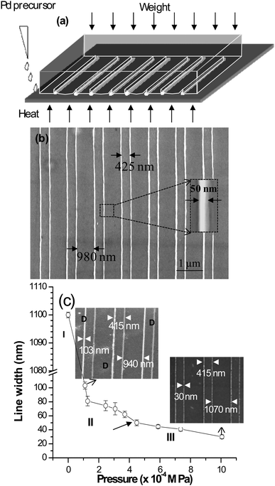 | ||
| Fig. 6 (a) Schematic showing the formation of nanochannels due to the near-complete microchannel roof collapse. (b) Large-area SEM micrograph of Pd-MNGP formed on Si substrate by NEM. Magnified view showing an individual nanowire of width 50 nm is shown in the inset. (c) Variation of the nanowire width with the external pressure applied on top of the PDMS stamp. In each case, the setup was heated at a ramp of 30 °C min−1 to 250 °C and held for 30 min. Here, zero pressure refers to the pressure due to the weight of the stamp itself (∼54 Pa), without any external pressure. SEM images corresponding to the pressures 110 Pa and 1010 Pa are also shown. The middle arrow refers to the pressure applied to obtain the pattern shown in (b) (from ref. 64). | ||
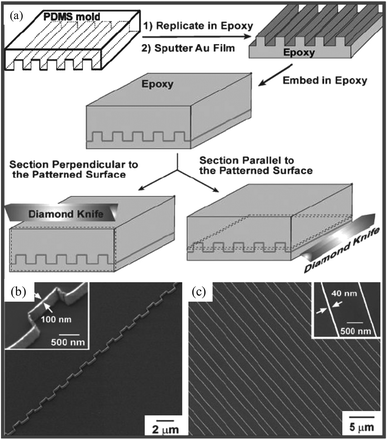 | ||
| Fig. 7 (a) Schematic illustration of the procedure used to fabricate complex nanostructures by sectioning a topographically patterned substrate (1-μm lines with 1-μm separation) positioned in two different orientations (relative to edge of the knife), (b) perpendicular-sectioning to the substrate (SiO2/Si) patterned with rectangular ridges leads to the formation of continuous stepped structures and (c) parallel-sectioning leads to Au-MNGP on a substrate (spacing, 1 μm) (from ref. 67). | ||
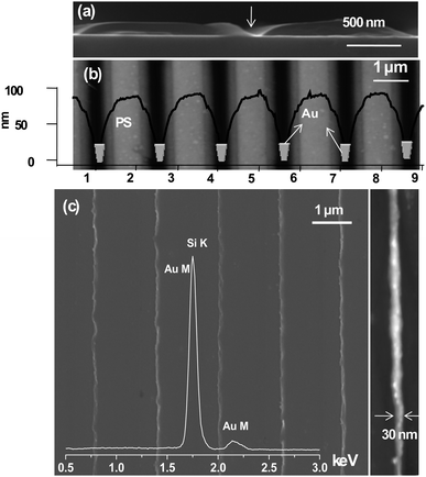 | ||
| Fig. 8 (a) Cross-section SEM image showing the nanogroove formation in polystyrene, (b) AFM image showing bright stripes gradually fading into dark grooves, and the z-profile of the pattern. (c) SEM image of a Au-MNGP formed by physical vapor deposition of the metal onto the polystyrene pattern followed by lift-off of the polymer in toluene. The EDS spectrum shows the Au M signal. AFM image of a single Au nanowire is shown alongside (from ref. 69). | ||
The combination of various techniques has been used to produce MNGPs. For example, patterned PDMS stamps have been used as phase-shifting masks to produce MNGPs down to 50 nm width.54 Edge transfer lithography, which is based on dewetting of the molecular ‘ink’ on the stamp, transfers the ink only along the edges to the substrate, thus producing fine lines of etch resist on metal, which could be transferred into MNGP by etching.71,72 Instead of patterned PDMS stamps which are prone to deformation, edge lithography can be performed using flat stamps but on patterned substrates. Geissler et al.73 produced Au-MNGPs of 140 nm width, exercising control of the spreading of the ink. A combination of capillary force lithography (CFL) and μCP has been shown to increase the resolution beyond what is achievable with either method. Au-MNGPs of 85 nm width have been obtained on an SiO2 substrate.74 Recently, a PDMS surface (patterned and unpatterned) glued to metallic nanostencil masks has been used for contact printing of meandering Au-MNGPs with a 50 nm line width.75 This process is essentially a combination of nanostencil printing and μCP. In another recent report,76 a combination of pulsed laser and NIL is reported as a direct one-step method for producing MNGPs. In this laser-assisted direct imprinting method, a single laser pulse passing through a transparent quartz mold melts the surface of the metal film. MNGPs of Au, Al, Cu and Ni up to 100 nm line width have been fabricated using this method.76
Another potential method of fabricating MNGPs is by self assembly. For example, Au-MNGPs were prepared by reducing a simple precursor (HAuCl4) inside a template formed by a self-assembled block copolymer.77 In order to guide self-assembly, trenches for the template formation were pre-defined using EBL. Exploiting periodic step structure of a CaF2 surface as a template, regular arrays of Ag nanoscale wires of width 5–7 nm and separation 20–50 nm have been obtained.78 Step edge decoration of a crystalline graphite surface has enabled nanowire electrodeposition for various metals with some control of periodicity.79
3. MNGP based device applications
MNGPs have been projected to have applications mainly in optical and electrical devices. Having devised a method to obtain MNGP, one of the major concerns is to achieve electrical conductivity close to the bulk metal which, given high concentrations of impurities introduced during the lithography process, can be a real challenge. In Fig. 3, near-metallic conductivity was achieved by annealing the obtained patterns above 250 °C.37 Instead of electrodes laid across the nanowire pattern, one may carry out conducting AFM measurements to examine the conducting nature of every single nanowire68 (Fig. 9). Well-conducting MNGPs with intentional gaps can serve as electrodes for molecular electronics, provided the substrate is electrically insulating. While high resolution techniques based on focused electron or ion beam are almost inevitable for patterning sub-100 nm ‘gaps’, these methods demand a conducting substrate to avoid broadening due to local charging. Using a variable pressure of water vapor (instead of vacuum), Dravid and coworkers have shown that intentional gaps (5–10 nm) can be produced in MNGPs laid on insulating substrates such as shown in Fig. 10.34 The nanogap electrode arrays are useful in building circuits based on large (bio)molecules and quantum dots.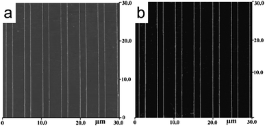 | ||
| Fig. 9 Conductance properties of Au-MNGP fabricated by nanotransfer edge printing. (a) AFM topography image and (b) the current map (from ref. 68). | ||
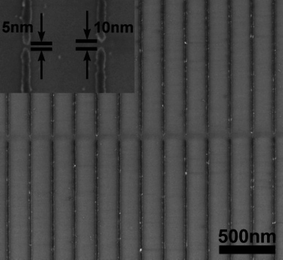 | ||
| Fig. 10 SEM image of Au/Pd-MNGP on a glass substrate showing lines with ∼20 nm width and 200 nm pitch, and intentional gaps of ∼5 and 10 nm (inset) (from ref. 34). | ||
One of the potent applications of MNGPs is in the field of solar cells, relating to the electrode material. The latter is required to be optically highly transparent for light transmission to the photovoltaic element and at the same time, electrically highly conducting for efficient collection of photogenerated charges. While coatings such as indium tin oxide (ITO), have been employed as transparent conducting materials, optimizing low sheet resistance with high capability to transmit light is not an easy task. Thus, there is a tradeoff between optical transparency and sheet resistance. Recently, the use of a metal nanowire mesh coating has also been proposed.80 Its comparison with ITO, as a case example, is given in Fig. 11.80 As shown, for an optical transparency ∼80%, typical sheet resistance of ITO is 10 Ω □−1. Ag-MNGPs with similar sheet resistances can have better optical transparency. Importantly, the authors reported 19% gain in solar conversion. Kang and Guo81 nanoimprinted MNGP's in the form of rectangular grids of Au, Cu and Al and examined sheet resistance and average transmittance in the visible range values as a function of metal line thickness, as shown in Fig. 12. While there is only a small difference (∼2%) in the transmittance trends exhibited by the MNGPs of different metals, there are noticeable differences in the sheet resistance. It increases with decreasing metal thickness; Au exhibits the least resistance ∼11.7 Ω □−1 at 40 nm line thickness with an average transmittance of ∼70%. An important feature of MNGPs is that the transparency can be increased without sacrificing the overall conductivity by using narrower and thicker metal lines. This is clearly an advantage over ITO or such electrodes, in which the sheet resistance has to be compromised to achieve high transmittance.
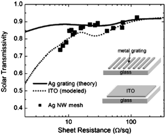 | ||
| Fig. 11 Solar photon flux-weighted transmissivity vs. sheet resistance for Ag-MNGPs (solid line), ITO (dotted line) and Ag nanowire meshes (squares) deposited on a glass substrate. The data for the Ag gratings were obtained by finite element modeling. The grating period (pitch) is 400 nm, the nanowire width is 40 nm, and its thickness is varied. The data for ITO are computed based on optical constants for e-beam deposited ITO acquired using spectroscopic ellipsometry. The data for Ag nanowire mesh data were obtained experimentally (adopted from ref. 80). | ||
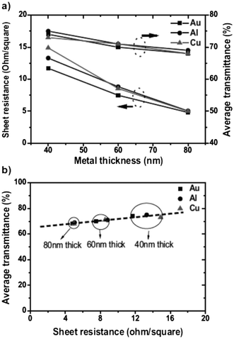 | ||
| Fig. 12 (a) Sheet resistance and average transmittance as a function of metal thickness in MNGPs of different metals; and (b) average transmittance vs. sheet resistance of semitransparent metal electrodes with a line width of 120 nm (from ref. 81). | ||
MNGP based light polarizers and beam splitters are emerging. MNGPs as subwavelength optical elements, have the potential to replace or improve conventional optical elements.82,83 Also, they can reduce the reflectivity at an interface, thus serving as anti-reflection coatings.84 The fine parallel metallic lines coated on a transparent substrate polarize efficiently when the width of the wires and the spacing are small compared to the wavelength of the incident light. For example in a MNGP, for a polarization direction perpendicular to the wire axis, the dipolar plasmon mode dominates the extinction spectrum. For a polarization parallel to the wire axis, the profile of the extinction spectrum varies mainly as a function of the grating constant (line spacing).85 The spectral position of the plasmon resonance can be tuned by an appropriate choice of nanowire geometry and material. Using NIL, Zhang et al.86 fabricated a polarizing beam splitter based on Al-MNGP, which exhibited uniform performance over broadband wavelengths with wide variations in the angle of incidence. As MNGPs require only narrow beams, compact designs are possible particularly important in optical telecommunication. There are designs involving embedded MNGPs which have been shown to serve as multifunctional optical devices.87 Employing MNGPs in nonlinear optical spectroscopy, highly sensitive molecular sensors have been realized.88 Besides high speed detection and sensitivity, the biomolecules may be detected without fluorescence tags.
Instead of creating MNGPs on flat substrates, Heath and coworkers have produced them suspended across a gap (Fig. 13), using the SNAP process.89,90 This setting of nanowires have been projected as a high-frequency nanomechanical resonator device. For the wires shown in Fig. 13, the measured frequency was ∼162.5 MHz, somewhat higher than the estimated value (99 MHz), the difference likely arising from the tension in the wires. The resonance frequency can be increased by narrowing the gap. The same group demonstrated the use of the SNAP process to fabricate ultradense crossbar circuits by repeating the imprinting process at 90° to the first. The crossbar configuration has emerged the circuit of choice for memristive device applications.59 In Fig. 14, the density of crossbar structures is in the range ∼1010–1011 junctions cm−2 amounting to pitch values in the 20–80 nm range. Using a mold patterned by SNAP in a repetitive NIL process, Williams and Heath59 joined by coworkers produced 34 nm pitch Pt crossbar structure (Fig. 14b), which in other words means 100 Gb cm−2! Step and flash imprint lithography (SFIL),91 a high-speed process involving photo NIL in sequential steps of UV flashes while laterally shifting the substrate, has also been used to fabricate high-density crossbar arrays each junction being 70 × 70 nm2.92 The crossbars have been successfully employed to produce memristive devices with applications in non-volatile memory.93
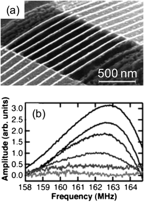 | ||
| Fig. 13 A high-frequency nanomechanical resonator fabricated by the SNAP process. (a) The resonator contains nine Pt nanowires 20 nm in diameter suspended over a 0.75 μm gap. (b) A resonance frequency of ∼162.5 MHz is monitored as a function of increasing magnetic field strength, from 0 to 5 T. The 0-field measurement is subtracted from each of the readings. The response increases with field strength, with the 5 T recording presented as the darkest trace (from ref. 89). | ||
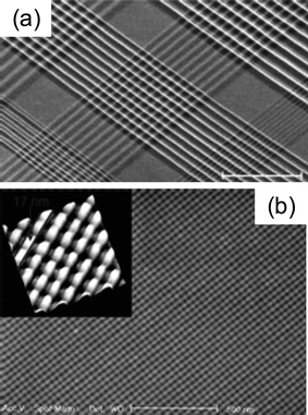 | ||
Fig. 14 (a) SEM image of a few hundred Pt nanowire crossbar circuits fabricated by repeating the SNAP process. The crossbars are fabricated from Pt nanowires with pitches ranging from 20 to 80 nm. The central crossbar has a junction density of ∼5 × 1010 cm−2, and the two crossbars to the lower left and right of this central one are at a junction density of ∼1011 cm−2 (from ref. 89). (b) The central region of a 13![[thin space (1/6-em)]](https://www.rsc.org/images/entities/char_2009.gif) 000 junction metal cross-bar structure. This circuit was generated by carrying out two consecutive nanoimprinting processes. The same mold was employed for both. The inset shows an AFM image of a magnified region of the cross bar (from ref. 59). 000 junction metal cross-bar structure. This circuit was generated by carrying out two consecutive nanoimprinting processes. The same mold was employed for both. The inset shows an AFM image of a magnified region of the cross bar (from ref. 59). | ||
As evident from the above discussion, there is greater emphasis in the literature to achieve finer lines (∼10 nm) with controllable thickness (10–100 nm) and spacing (few tens to few hundreds of nm), increasing the applicability of MNGPs. Every year, newer methods are being developed to meet these requirements and bring out MNGPs suitable in a given application, be it in solar cells, anti-reflective surfaces, electrode junctions etc. Applications in flexible and optoelectronics are also foreseen. Thus, the field of MNGPs is growing rapidly.
4. Conclusions
This article has sourced a number of examples, not exhaustive of course, of metal nanowire patterning from the current literature under the title theme, MNGP. Most of them rely on lithography techniques to produce MNGPs, encompassing AFM, e and ion beam, optical, imprint as well as soft stamping methods in addition to many hybrid methods. Linewidths below 10 nm and spacings, few tens to few hundreds of nms have been achieved over the wafer scale. While most examples belong to noble and semi-noble metals, there have been reports on reactive metals (Al, Ti, Cu, W etc.) as well. MNGPs with zig-zag or aperiodic geometries are immediate possibilities for the future. Wide ranging applications based on MNGPs are envisaged—nanogap and crossbar electrode arrays, nanomechanical resonators, transparent conducting electrodes, high sensitive molecular detectors, polarizing optical elements requiring narrow beams, and so on. Conventional grating patterns which possess linewidths and spacings up to few μm, are already well known in biosensing.94,95 However, we have not embarked on such examples, as this topic is outside the scope of the article. We have also not dealt with atomically thin nanowires,96 of serious interest in quantum conductance.4 The nanowires covered in this article fall in the metallic regime, but thin enough for the surface plasmons to be dominant. Such MNGPs should have immense impact in futuristic technologies, particularly telecommunication, biosensing and ultra high density memory devices, nanoscale optoelectronic switches.97Acknowledgements
The authors thank Professor C. N. R. Rao for encouragement. Support from Department of Science and Technology, Government of India is gratefully acknowledged. The authors appreciate and acknowledge the contributions of various researchers whose work has formed the content of this review. Radha B. thanks CSIR for financial assistance.References
- C. N. R. Rao, A. Govindaraj, Nanotubes and Nanowires, The Royal Society of Chemistry, London, 2005 Search PubMed.
- Nanowires and Nanobelts: Materials, Properties and Devices, ed. Z. L. Wang, Kluwer Academic Publishers, USA, 2003 Search PubMed.
- C. J. Murphy, T. K. Sau, A. M. Gole, C. J. Orendorff, J. Gao, L. Gou, S. E. Hunyadi and T. Li, J. Phys. Chem. B, 2005, 109, 13857–13870 CrossRef CAS.
- W. A. deHeer, S. Frank and D. Ugarte, Z. Phys. B: Condens. Matter, 1997, 104, 469–473 CrossRef CAS.
- S. Link and M. A. El-Sayed, J. Phys. Chem. B, 1999, 103, 8410–8426 CrossRef CAS.
- A. G. Umnov, Y. Shiratori and H. Hiraoka, Appl. Phys. A: Mater. Sci. Process., 2003, 77, 159–161 CrossRef CAS.
- X. S. Fang, Y. Bando, U. K. Gautam, C. Ye and D. Golberg, J. Mater. Chem., 2008, 18, 509–522 RSC.
- K. Changwook, G. Wenhua, B. Martha, M. R. Ian, C. Hyungsoo and K. Kyekyoon, Adv. Mater., 2008, 20, 1859–1863 CrossRef CAS.
- M. Kast, P. Schroeder, Y. J. Hyun and P. Pongratz, Nano Lett., 2007, 7, 2540–2544 CrossRef CAS.
- E. P. Lee, Z. Peng, D. M. Cate, H. Yang, C. T. Campbell and Y. Xia, J. Am. Chem. Soc., 2007, 129, 10634–10635 CrossRef CAS.
- F. Li, M. Zhu, C. Liu, W. L. Zhou and J. B. Wiley, J. Am. Chem. Soc., 2006, 128, 13342–13343 CrossRef CAS.
- X. Li, G. Song, Z. Peng, X. She, J. Li, J. Sun, D. Zhou, P. Li and Z. Shao, Nanoscale Res. Lett., 2008, 3, 521–523 Search PubMed.
- Y. Yoo, K. Seo, S. Han, K. S. K. Varadwaj, H. Y. Kim, J. H. Ryu, H. M. Lee, J. P. Ahn, H. Ihee and B. Kim, Nano Lett., 2010, 10, 432, DOI:10.1021/nl903002x.
- Unlike semiconductor nanowires, where heterostructuring is common with vertically grown wires; see for example: F. Hong Jin, W. Peter and Z. Margit, Semiconductor Nanowires: From Self-Organization to Patterned Growth, Small, 2006, 2, 700–717 Search PubMed; X. S. Fang, Y. Bando, U. K. Gautam, T. Y. Zhai, S. Gradecak and D. Golberg, J. Mater. Chem., 2009, 19, 5683–5689 CrossRef CAS.
- K. Kim and S. M. Cho, Proc. IEEE Sens., 2004, 1–3, 705–707 Search PubMed.
- S. Cherevko, X. Xing and C.-H. Chung, ECS Meeting Abstracts, 2009, vol. 902, pp. 3130–3130 Search PubMed.
- J.-H. Kim, S. Khanal, M. Islam, A. Khatri and D. Choi, Electrochem. Commun., 2008, 10, 1688–1690 CrossRef CAS.
- A. D. Franklin, M. R. Maschmann, M. DaSilva, D. B. Janes, T. S. Fisher and T. D. Sands, J. Vac. Sci. Technol., B, 2007, 25, 343–347 CrossRef CAS.
- Y. J. Chen, J. H. Hsu and H. N. Lin, Nanotechnology, 2005, 16, 1112–1115 CrossRef CAS.
- S. Hu, A. Hamidi, S. Altmeyer, T. Koster, B. Spangenberg and H. Kurz, J. Vac. Sci. Technol., B, 1998, 16, 2822–2824 CrossRef CAS.
- S. F. Lyuksyutov, R. A. Vaia, P. B. Paramonov, S. Juhl, L. Waterhouse, R. M. Ralich, G. Sigalov and E. Sancaktar, Nat. Mater., 2003, 2, 468–472 CrossRef CAS.
- C. Martin, G. Rius, X. Borrise and F. Perez-Murano, Nanotechnology, 2005, 16, 1016–1022 CrossRef CAS.
- M. Rolandi, C. F. Quate and H. Dai, Adv. Mater., 2002, 14, 191–194 CrossRef CAS.
- S. G. David, Z. Hua and A. M. Chad, Angew. Chem., Int. Ed., 2004, 43, 30–45 CrossRef.
- P. J. Thomas, G. U. Kulkarni and C. N. R. Rao, J. Mater. Chem., 2004, 14, 625–628 RSC.
- R. D. Piner, J. Zhu, F. Xu, S. Hong and C. A. Mirkin, Science, 1999, 283, 661–663 CrossRef CAS.
- H. Zhang and C. A. Mirkin, Chem. Mater., 2004, 16, 1480–1484 CrossRef CAS.
- A. A. Tseng, S. Jou, A. Notargiacomo and T. P. Chen, J. Nanosci. Nanotechnol., 2008, 8, 2167–2186 CrossRef CAS.
- K. Keun-Ho, M. Nicolaie and D. E. Horacio, Small, 2005, 1, 632–635 CrossRef CAS.
- K. Salaita, Y. Wang and C. A. Mirkin, Nat. Nanotechnol., 2007, 2, 145–155 CrossRef CAS.
- J. F. Liu and G. P. Miller, Nanotechnology, 2009, 20, 055303 CrossRef.
- F. Lehmann, G. Richter, T. Borzenko, V. Hock, G. Schmidt and L. W. Molenkamp, Microelectron. Eng., 2003, 65, 327–333 CrossRef CAS.
- A. E. Grigorescu and C. W. Hagen, Nanotechnology, 2009, 20, 292001 CrossRef CAS.
- B. D. Myers and V. P. Dravid, Nano Lett., 2006, 6, 963–968 CrossRef CAS.
- J. Joo, B. Y. Chow and J. M. Jacobson, Nano Lett., 2006, 6, 2021–2025 CrossRef CAS.
- M. H. V. Werts, M. Lambert, J.-P. Bourgoin and M. Brust, Nano Lett., 2002, 2, 43–47 CrossRef CAS.
- T. Bhuvana and G. U. Kulkarni, ACS Nano, 2008, 2, 457–462 CrossRef CAS.
- E. U. Donev and J. T. Hastings, Nano Lett., 2009, 9, 2715–2718 CrossRef CAS.
- L. Rotkina, J. F. Lin and J. P. Bird, Appl. Phys. Lett., 2003, 83, 4426–4428 CrossRef CAS.
- S. Reyntjens and R. Puers, J. Micromech. Microeng., 2001, 11, 287–300 CrossRef CAS.
- K. Zhao, R. S. Averback and D. G. Cahill, Appl. Phys. Lett., 2006, 89, 053103–053103 CrossRef.
- O. V. Mena, V. Savu, K. Sidler, G. Villanueva, M. A. F. van den Boogaart and J. Brugger, in Nano/Micro Engineered and Molecular Systems, 2008, 3rd IEEE International Conference, pp. 807–811 DOI:10.1109/NEMS.2008.4484447.
- C. X. Xiang, Y. G. Yang and R. M. Penner, Chem. Commun., 2009, 859–873 RSC.
- E. J. Menke, M. A. Thompson, C. Xiang, L. C. Yang and R. M. Penner, Nat. Mater., 2006, 5, 914–919 CrossRef CAS.
- C. Xiang, S.-C. Kung, D. K. Taggart, F. Yang, M. A. Thompson, A. G. Güell, Y. Yang and R. M. Penner, ACS Nano, 2008, 2, 1939–1949 CrossRef CAS.
- G. M. Wallraff and W. D. Hinsberg, Chem. Rev., 1999, 99, 1801–1822 CrossRef CAS.
- B. Wu and A. Kumar, J. Vac. Sci. Technol., B, 2007, 25, 1743–1761 CrossRef CAS.
- J. Koch, E. Fadeeva, M. Engelbrecht, C. Ruffert, H. H. Gatzen, A. Ostendorf and B. N. Chichkov, Appl. Phys. A: Mater. Sci. Process., 2006, 82, 23–26 CrossRef CAS.
- H. H. Solak, C. David, J. Gobrecht, V. Golovkina, F. Cerrina, S. O. Kim and P. F. Nealey, Microelectron. Eng., 2003, 67–68, 56–62 CrossRef CAS.
- V. Auzelyte, H. H. Solak, Y. Ekinci, R. MacKenzie, J. Voros, S. Olliges and R. Spolenak, Microelectron. Eng., 2008, 85, 1131–1134 CrossRef CAS.
- K. Miyoshi, Y. Aoki, T. Kunitake and S. Fujikawa, Langmuir, 2008, 24, 4205–4208 CrossRef CAS.
- H. Zhang, M. Tang, J. McCoy and T.-H. Her, Opt. Express, 2007, 15, 5937–5947 CrossRef CAS.
- A. B. Kahng and Y. C. Pati, in Proc. Intl. Symp. Phys. Des., ACM, Monterey, California, United States, 1999 Search PubMed.
- S. Y. Chou, P. R. Krauss and P. J. Renstrom, Science, 1996, 272, 85–87 CrossRef CAS.
- J.-H. Lee, K.-y. Yang, S.-H. Hong, H. Lee and K.-W. Choi, Microelectron. Eng., 2008, 85, 710–713 CrossRef CAS.
- G.-Y. Jung, Z. Li, W. Wu, S. Ganapathiappan, X. Li, D. L. Olynick, S. Y. Wang, W. M. Tong and R. S. Williams, Langmuir, 2005, 21, 6127–6130 CrossRef CAS.
- E. U. Kim, K. J. Baeg, Y. Y. Noh, D. Y. Kim, T. Lee, I. Park and G. Y. Jung, Nanotechnology, 2009, 20, 355302 CrossRef.
- S. H. Ko, I. Park, H. Pan, C. P. Grigoropoulos, A. P. Pisano, C. K. Luscombe and J. M. J. Frechet, Nano Lett., 2007, 7, 1869–1877 CrossRef CAS.
- G.-Y. Jung, E. Johnston-Halperin, W. Wu, Z. Yu, S.-Y. Wang, W. M. Tong, Z. Li, J. E. Green, B. A. Sheriff, A. Boukai, Y. Bunimovich, J. R. Heath and R. S. Williams, Nano Lett., 2006, 6, 351–354 CrossRef CAS.
- M. Geissler, H. Wolf, R. Stutz, E. Delamarche, U.-W. Grummt, B. Michel and A. Bietsch, Langmuir, 2003, 19, 6301–6311 CrossRef CAS.
- A. W. Jens, H. Mahiar and I. Olle, Adv. Funct. Mater., 2008, 18, 2563–2571 CrossRef.
- Y. Xia and G. M. Whitesides, Angew. Chem., Int. Ed., 1998, 37, 551–575 CrossRef CAS.
- B. D. Gates, Q. Xu, J. C. Love, D. B. Wolfe and G. M. Whitesides, Annu. Rev. Mater. Res., 2004, 34, 339–372 CrossRef CAS.
- B. Radha and G. U. Kulkarni, Small, 2009, 5, 2271–2275 CrossRef CAS.
- Q. Xu, B. D. Gates and G. M. Whitesides, J. Am. Chem. Soc., 2004, 126, 1332–1333 CrossRef CAS.
- Q. Xu, R. M. Rioux and G. M. Whitesides, ACS Nano, 2007, 1, 215–227 CrossRef CAS.
- Q. Xu, R. M. Rioux, M. D. Dickey and G. M. Whitesides, Acc. Chem. Res., 2008, 41, 1566–1577 CrossRef CAS.
- M. Q. Xue, Y. L. Yang and T. B. Cao, Adv. Mater., 2008, 20, 596–600 CrossRef CAS.
- B. Radha and G. U. Kulkarni, ACS Appl. Mater. Interfaces, 2009, 1, 257–260 Search PubMed.
- Y. S. Kim and H. H. Lee, Adv. Mater., 2003, 15, 332–334 CrossRef CAS.
- O. Cherniavskaya, A. Adzic, C. Knutson, B. J. Gross, L. Zang, R. Liu and D. M. Adams, Langmuir, 2002, 18, 7029–7034 CrossRef CAS.
- R. B. A. Sharpe, B. J. F. Titulaer, E. Peeters, D. Burdinski, J. Huskens, H. J. W. Zandvliet, D. N. Reinhoudt and B. Poelsema, Nano Lett., 2006, 6, 1235–1239 CrossRef CAS.
- M. Geissler, J. M. McLellan and Y. Xia, Nano Lett., 2005, 5, 31–36 CrossRef CAS.
- D. Xuexin, Z. Yiping, P. András, B. Erwin, N. R. David and H. Jurriaan, Adv. Funct. Mater., 2010, 20, 663, DOI:10.1002/adfm.200901700.
- L. Min Hyung, Y. L. Julia and W. O. Teri, Angew. Chem., Int. Ed., 2010, 49, 3057–3060, DOI:10.1002/anie.200906800.
- B. Cui, C. Keimel and S. Y. Chou, Nanotechnology, 2010, 21, 045303 CrossRef.
- J. Chai, D. Wang, X. Fan and J. M. Buriak, Nat. Nanotechnol., 2007, 2, 500–506 CrossRef.
- M. Batzill, M. Sarstedt and K. J. Snowdon, Nanotechnology, 1998, 9, 20–29 CrossRef CAS.
- C. W. Erich, P. Z. Michael, F. Frédéric, J. M. Benjamin, I. Koji, C. H. John and M. P. Reginald, ChemPhysChem, 2003, 4, 131–138 CrossRef CAS.
- J. Y. Lee, S. T. Connor, Y. Cui and P. Peumans, Nano Lett., 2008, 8, 689–692 CrossRef CAS.
- M. G. Kang and L. J. Guo, Adv. Mater., 2007, 19, 1391–1396 CrossRef CAS.
- S. Y. Chou, in Lasers and Electro-Optics Society, The 15th Annual Meeting of the IEEE, 2002, pp. 574–575, vol. 572 Search PubMed.
- H. J. Zhao, Y. J. Peng, J. Tan, C. R. Liao, P. Li and X. X. Ren, Chin. Phys. B, 2009, 18, 5326 Search PubMed.
- N. F. Hartman and T. K. Gaylord, Appl. Opt., 1988, 27, 3738–3743 CrossRef CAS.
- G. Schider, J. R. Krenn, W. Gotschy, B. Lamprecht, H. Ditlbacher, A. Leitner and F. R. Aussenegg, J. Appl. Phys., 2001, 90, 3825–3830 CrossRef CAS.
- L. Zhang, C. F. Li, J. Li, F. Zhang and L. Shi, J. Optoelectron. Adv. M., 2006, 8, 847–850 Search PubMed.
- W. Liu, Y. Zeng, L. Chen, D. L. Wang and Q. M. Xiao, Appl. Opt., 2008, 47, 4874–4877 CrossRef CAS.
- K. Okamoto, Z. Zhang, D. T. Wei and A. Scherer, Thin Solid Films, 2004, 469–470, 420–424 CrossRef CAS.
- N. A. Melosh, A. Boukai, F. Diana, B. Gerardot, A. Badolato, P. M. Petroff and J. R. Heath, Science, 2003, 300, 112–115 CrossRef CAS.
- J. R. Heath, Acc. Chem. Res., 2008, 41, 1609–1617 CrossRef CAS.
- D. J. Resnick, S. V. Sreenivasan and C. G. Willson, Mater. Today, 2005, 8, 34–42 CrossRef CAS.
- D. K. Yun, K. D. Kim, S. Kim, J. H. Lee, H. H. Park, J. H. Jeong, Y. K. Choi and D. G. Choi, Nanotechnology, 2009, 20 Search PubMed.
- J. J. Yang, M. D. Pickett, X. Li, A. A. OhlbergDouglas, D. R. Stewart and R. S. Williams, Nat. Nanotechnol., 2008, 3, 429–433 CrossRef CAS.
- P. Fiori and M. Paige, Anal. Biochem., 2004, 380, 339–342 CAS.
- J.-N. Yih, Y.-M. Chu, Y.-C. Mao, W.-H. Wang, F.-C. Chien, C.-Y. Lin, K.-L. Lee, P.-K. Wei and S.-J. Chen, Appl. Opt., 2006, 45, 1938–1942 CrossRef CAS.
- C. Ludovico and A. O. Geoffrey, Adv. Mater., 2009, 21, 1013–1020 CrossRef CAS.
- S. Gaweda, A. Podborska, W. Macyk and K. Szacilowski, Nanoscale, 2009, 1, 299–316 RSC.
| This journal is © The Royal Society of Chemistry 2010 |