Reliable signal processing using parallel arrays of non-identical nanostructures and stochastic resonance
Javier
Cervera
*,
José A.
Manzanares
and
Salvador
Mafé
Facultat de Física, Universitat de València, E-46100 Burjassot, Spain. E-mail: Javier.Cervera@uv.es
First published on 20th May 2010
Abstract
In the stochastic resonance (SR) phenomena, the response of a non-linear system to a weak periodic input signal is optimised by the presence of a particular level of noise which enhances signal detection. We explore, theoretically, the influence of thermal noise in arrays of metal nanoparticles functionalised with organic ligands acting as tunnelling junctions, with emphasis on the interplay between the SR phenomena and the nanostructure variability. In this system, the transference of a reduced number of electrons may suffice to implement a variety of electronic functions. However, because nanostructures are expected to show a significant variability in their physical characteristics, it is important to study the relation between the diversity-induced static noise and the dynamic noise caused by thermal fluctuations. We consider an ideal model based on the Coulomb blockade and tunnelling effects that includes the stochastic nature of electron transference due to thermal noise together with the nanostructure variability found in experimental distribution functions. The correlation between the input (potential) and the output (current) signals, as well as the absolute value of the current and its time fluctuations, are analysed as a function of the temperature and the number of nanostructures. Extensive kinetic Monte Carlo simulations suggest that the interplay between thermal noise and variability could permit reliable processing of weak signals with many non-identical nanostructures.
1. Introduction
In the stochastic resonance (SR) phenomenon, the response of a non-linear system to a weak periodic input signal is optimised by the presence of a particular level of noise which enhances signal detection.1 This occurs in a wide variety of natural (e.g., sensory neurons) and artificial (e.g., microelectronic circuits) systems.1–4 However, for SR to be effective in a single unit system, the noise intensity must be adjusted to a particular level that depends on the nature of the input signal, and this constitutes a serious practical limitation. Remarkably, non-linear dynamical systems composed of many identical units can detect weak, sub-threshold input signals irrespective of the particular noise level (molecular-scaled biological networks, for instance, operate correctly in a noisy environment).2,4,5 However, real units are not identical in most practical cases (biochemical systems, nanostructures, and social groups show high variability in their individual characteristics) and then the interplay between diversity and SR naturally arises.6 This is a crucial issue for nanodevice design and application because of the weak signals involved and the high variability of the individual nanostructures. This variability acts as a static noise to be added to the dynamic noise caused by thermal fluctuations.7–10Logical and signal processing nanodevices based on the transport of a small number of electrons have attracted great interest due to the continuous miniaturisation of electronics.11–13 For instance, the tunnelling current through a gold colloid quantum dot between two electrodes could be modulated by the attached ligands, forming a nanoparticle (NP)-based single electron transistor whose tunnelling barriers are defined by monolayers of thiols.14 We have considered recently the synchronisation of coupled single-electron circuits whose building blocks are NPs functionalised with organic ligands that act as tunnelling junctions.15 The tunnel junction acts as a leaky capacitor that can be controlled by the voltage across the junction and, because of the scale at which transport occurs, the transference of a few electrons may suffice to implement a variety of electronic functions.12 Electron tunnelling is influenced by the discrete nature of charge transport and the Coulomb blockade energy barrier, which must be higher than the thermal energy for the transport of single electrons to be controlled. This condition is usually fulfilled by scaling down to the nanoscale where the problems of thermal noise and nanostructure variability cannot be ignored. In particular, the size distribution of the metal NPs16 results in a significant spread of their properties. It has been reported that the high parameter variability influences the conductance of molecular memories,17 the threshold potential of voltage-driven molecular switches,18 and the tunnelling junction characteristics of disordered arrays.19 Fault-tolerant approaches8–10,20,21 are needed to perform reliable information processing from inherently unreliable nanostructures. Recently, we have explored theoretically the application of nanoscale switches to implement a signal processing scheme and a frequency-dependent associative memory,22 paying attention to the effects of the nanostructure tolerance and the thermal fluctuations.8
Metal NPs functionalised with organic ligands14,23–28 can be employed to modulate the electron transfer between the electrodes in molecular circuits.22,29 Tunnelling is the dominant conduction mechanism through alkanethiol ligands,30,31 although the nature of the electrical contacts in the molecular junctions is also important.31 An array of nanostructures whose building blocks are metal NPs interconnected with tunnelling junctions is an idealisation of nanoscale circuits based on the Coulomb blockade effect2,4 that includes the stochastic nature of electron transference together with the nanostructure variability typically found in experimental systems. An electron crossing the nanostructure must go first from the electrode to the NP (co-tunnelling is neglected). However, at 0 K, due to the Coulomb blockade effect, electron transfer from one electrode to the (uncharged) NP can only occur when the applied voltage V0 between the electrodes is higher than the threshold value Vth = e/2CR. This process is characterised by the signal-to-threshold distance (Vth − V0). Negative values the of signal-to-threshold distance correspond to supra-threshold signals while positive values correspond to sub-threshold signals.5
We analyse here the processing of a weak (sub-threshold) input signal V(t) using a parallel array of N nanostructures whose building blocks are metal NPs interconnected with tunnelling junctions. The output is the total current I(t) through the N nanostructures. The signal processing is based on the fact that, at finite temperatures, the output shows a positive correlation with the input, even for sub-threshold input signals. However, since the currents generated by sub-threshold input signals are very small, in addition to a positive correlation, the absolute value of the current and its time fluctuations are also crucial for signal processing reliability. The practical implementations of logical and signal processing schemes with nanodevices are expected to have a low reliability because of the weak signals involved, the thermal noise and the nanostructure variability. Using kinetic Monte Carlo simulations, we study the effects of thermal noise on the signal processing nanostructures whose basic properties have been demonstrated experimentally.14,23–28 Special attention is paid to the SR phenomena in relation to the enhancement of the signal processing reliability. In addition, since nanostructures are expected to show a significant variability in their physical characteristics, we study the interplay between the “dynamic noise” caused by thermal fluctuations and the “static noise” associated with the nanostructure variability.
This study has been partially motivated by previous theoretical findings on SR phenomena with different systems and conditions.2,4,5 The rapid increase of the correlation coefficient C with the temperature at low T, the slow decrease of C at high T, and the increase of C with the number of nanostructures in the array have been verified experimentally with GaAs-based nanowire field-effect transistors.3 The effect of the variability in the physical characteristics was considered in ref. 6 for a (hypothetical) system of coupled threshold units with significant threshold heterogeneity driven by an external periodic signal. It was found that an appropriate level of diversity can improve the system response to the input signal and this result led to speculate that the diversity present in some biological systems could have an important function.6 We will consider also the interplay between the thermal noise and the nanostructure variability in the processing of weak signals.
2. Theoretical model
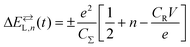
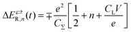
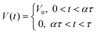
The nanostructure of Fig. 1a is formed by a metal NP linked to the electrodes by organic ligands acting as tunnelling junctions.22 The equivalent circuit of this nanostructure is shown in Fig. 1b. The left and right ligands have tunnelling resistances RL and RR that are much higher than the quantum resistance R0 = h/e2 = 26kΩ, where e is the elementary charge and h is the Planck constant. The electron transfer can be described by the equations:22,32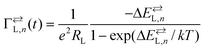 | (1) |
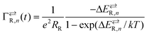 | (2) |
 | (3) |
 | (4) |
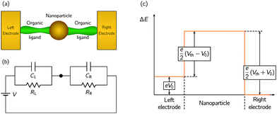 | ||
| Fig. 1 Scheme of the nanostructure composed of a metal NP linked to the electrodes by organic ligands acting as tunnelling junctions (a), the equivalent circuit of the system (b) and the electrostatic energy diagram of the electron for a sub-threshold voltage V0 in the case CL = CR (c). The diagram corresponds to an uncharged NP and shows an energy barrier separating two stable states of low energy, as typical of SR systems. | ||
The applied voltage between the electrodes has a modulation of period τ. The voltage is in the ON state (V0) during a fraction α of this period so that V(t) = V(t + τ) and
 | (5) |
 | (6) |
 | (7) |
3. Results and discussion
The kinetic Monte Carlo simulations have been carried out with the parameter values (see Fig. 1a): RR = 108 Ω, RL = 107 Ω and CL = CR = 2 aF, so that Vth = 40 mV. These can be considered as typical values for the nanostructure considered.8,15,24–28 The voltage modulation of eqn (5) has amplitude V0 = 5 mV unless otherwise specified, period τ = 10 μs and α = 0.1. The time interval to calculate the current is Δt = 0.1 μs and the total simulation time is t0 = 1 ms.Fig. 2a shows the correlation coefficient C vs. the temperature T for different numbers of nanostructures. At low temperatures, the Coulomb blockade prevents the electron transfer so that both I and C vanish. At T∼50 K, the thermal energy kT leads to a significant increase of the tunnelling rates, allowing the electrons to cross the nanostructure and give a correlation significantly different from zero. The correlation coefficient increases with the temperature until it reaches a maximum. A further increase of T gives a slow decrease of C because of the increase in the amplitude of the thermal fluctuations of the current. This behaviour is qualitatively similar for each N, although the initial increase and the maximum value of C are slightly shifted to the low temperature region with the increase of N. Fig. 2b shows the effect of the applied voltage V0 on C for N = 1. As expected, increasing V0 up to the threshold potential Vth = 40 mV improves correlation (and hence the signal processing reliability).
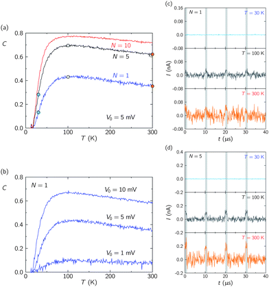 | ||
| Fig. 2 Correlation coefficient C vs. temperature T for different numbers of nanostructures N (with V0 = 5 mV) (a) and applied sub-threshold voltages V0 (with N = 1) (b). Time response curves of the current for different temperatures with N = 1 (c) and 5 (d). The curves correspond to the temperatures marked by the six dots in the C vs. T curves of (a). The narrow bands (in grey) correspond to time intervals with the ON voltage (V = V0) whereas the wide regions between the bands correspond to intervals with the OFF voltage (V = 0). | ||
Fig. 2a shows that an optimal level of thermal noise helps to improve the processing of sub-threshold potentials and that this phenomenon is enhanced by increasing the number of nanostructures, in agreement with previous studies emphasising neural networks.2,4,5 The rapid increase of the correlation coefficient with the temperature at low T, the slow decrease of C at high T, and the increase of C with the number of nanostructures in the array are characteristics of the SR phenomena.2–5 However, a serious issue in practical design not fully addressed in previous studies is that significant correlations do not necessarily mean high output currents (compared to the current fluctuations) if weak input signals are involved. Therefore, the current and its time fluctuations should also be considered for the signal processing reliability. Fig. 2c and 2d show the time response curves of the total current for different temperatures with N = 1 (c) and 5 (d). The narrow bands (in grey) indicate the time intervals with the ON voltage (V = V0) whereas the wide regions between bands indicate the intervals with the OFF voltage (V = 0). The results correspond to the temperatures marked by the six dots in the C vs. T curves of Fig. 2a. The curves of Fig. 2c and 2d give the electric current I and show the time structure of the correlation. For N = 1, only the time averaging can assist correlation because the interval Δt = 0.1 μs is much higher than the typical time for individual electron transfer. For N > 1, however, the calculated current also includes the effect of averaging over the number of nanostructures and this leads to a better correlation. As to the temperature effect, comparison of the current vs. time curves for T = 100 K and 300 K shows that I is higher at 300 K than at 100 K but so are the current fluctuations, and this worsens the correlation.
A reliable processing relies on sufficiently long time averaging so that random fluctuations are screened out. It is therefore mandatory to analyse also the effect of the averaging time Δt on the correlation coefficient. This is done in Fig. 3a and 3b for N = 5. The time response curves of Fig. 3b are obtained at T = 100 K and correspond to the three dots marked in Fig. 3a. Because the current is defined as I = ΔQ/Δt, high values of Δt correspond to long time averages of the charge ΔQ delivered by the nanostructures. Clearly, long time averaging decreases significantly the current fluctuations, allowing for significant correlations for Δt = 0.1 μs. This effect is similar to that noted in Fig. 2a for the number of nanostructures. Note that the ideal, limiting value C = 1 could not be attained because of the noise and finite-size effects. However, much higher Δt or, alternatively, a higher number N of nanostructures, should increase the correlation further.
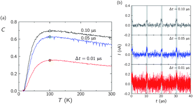 | ||
| Fig. 3 C vs. temperature T for different times Δt and N = 5 with V0 = 5 mV (a). Time response curves of the current at 100 K for the times Δt shown in the curves (b). Because the current is defined as I = ΔQ/Δt, high values of Δt correspond to long time averages of the charge ΔQ. | ||
Fig. 2 and 3 have emphasised that thermal noise can provide the electrons with the necessary energy to cross the nanostructure, allowing correlation even in the region of sub-threshold potentials. This is reminiscent of the results obtained previously for a network of FitHugh-Nagumo model neurons subjected to different individual noises:5 the cooperative effect of the neural network allowed correct signal retrieval all over the range of signal-to-threshold distances provided that the operational temperature was high enough. To better analyse this unique property of SR,5Fig. 4a shows the correlation coefficient C vs. the normalised signal-to-threshold distance (Vth − V0)/Vth for different temperatures T with N = 10 and Δt = 0.1 μs. It is observed that the thermal noise does not disturb the array capability to process the supra-threshold signals while the increase of this noise enhances the sub-threshold processing.
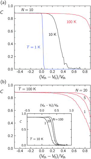 | ||
| Fig. 4 (a) Correlation coefficient C vs. the normalised signal-to-threshold distance (Vth − V0)/Vth for different temperatures T with N = 10 and Δt = 0.1 μs. (b) C vs. (Vth − V0)/Vth for different numbers N and Δt = 0.1 μs at T = 100 K. The inset shows the effect of N in the values of C for T = 10 K. The increase in the number of nanostructures (system redundancy) improves significantly the system performance (see also Fig. 2a) although the thermal noise is still necessary for significant correlation in the case of sub-threshold potentials V0 < Vth. | ||
Fig. 4b shows the correlation coefficient C vs. (Vth − V0)/Vth for different numbers N with Δt = 0.1 μs and T = 100 K (the inset shows the effect of N on C for T = 10 K). As in the case of the thermal noise, the increase in the number of nanostructures (system redundancy) improves significantly the performance of the system, although the thermal noise is still necessary for correct signal processing (see Fig. 2a). Therefore, weak, sub-threshold signals can still be processed at high enough temperatures by increasing the number of nanostructures in the array because averaging enhances the sensitivity.4,5
The peak of C in Fig. 2 and Fig. 3 could be observed at higher temperatures by decreasing the nanostructure dimensions. The use of ligand-stabilized metal nanoclusters a few nanometres in radii enable effective capacitances of the order of 10−18 F = 1 aF, and then the Coulomb blockade effect appears at close to ambient temperatures.14,24–28 In fact room-temperature solutions of nanoclusters with monodisperse cores display electrochemical Coulomb staircases because of the sub-attofarad double layer capacitances.24
So far we have analysed arrays of identical nanostructures. However, one of the salient characteristics of nanoscale systems is their relatively high variability,7–10 which should affect their response to a common input signal. For instance, if the capacitance CR of Fig. 1a is different for each nanostructure in the parallel array, the threshold voltages Vth = e/2CR will also be different, and this could change the correlation between the output current and the input potential. To study the effect of variability, we have considered arrays of N = 10 and 100 non-identical nanostructures where the values of the physical parameters (CR, CL, RR and RL) follow a random distribution. For instance, the N values of the capacitance CR would be randomly distributed within the range 1 − δ ≤ CR/C0R ≤ 1 + δ where C0R is the central value and 2δ is the width of the distribution for the CR/C0R values. The central values (R0R = 108 Ω, R0L = 107 Ω and C0R = C0L = 2 aF) are those used in Fig. 2–4. For every variability δ, the correlation coefficient is calculated 100 times with different individual values of the physical parameters distribution. The points shown in Fig. 5a and 5b are average results.
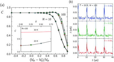 | ||
| Fig. 5 (a) C vs. (Vth − V0)/Vth for the variability widths δ = 0 (orange circles), 0.25 (green squares) and 0.50 (blue triangles) in the cases of N = 10 and 100 nanostructures at T = 20 K. The inset shows the C vs. δ curves for different temperatures with V0 = 5 mV and N = 100 (note the correspondence between the marked points in the curve for T = 20 K and the C vs. (Vth − V0)/Vth curves for N = 100). The physical parameters of each nanostructure follow a random distribution of relative width δ. (b) The time response curves of the total current I for the three values of the variability width considered in (a) and N = 100. | ||
Fig. 5a shows the correlation coefficient C vs. (Vth − V0)/Vth for the variability widths δ = 0 (orange circles), 0.25 (green squares) and 0.50 (blue triangles) in the cases of N = 10 and 100 nanostructures at T = 20 K. The inset shows the C vs.δ curves for different temperatures with V0 = 5 mV and N = 100 (note the correspondence between the points marked on the curve for T = 20 K and the C vs. (Vth − V0)/Vth curves for N = 100 of Fig. 5a). Finally, Fig. 5b shows the time response curves of the total current I for N = 100 and the three values of δ in the curve for T = 20 K of the inset in Fig. 5a.
Fig. 5a shows that the correlation is robust to the variability effect even for weak, sub-threshold inputs. The inset in this figure emphasises this effect showing that the nanostructure variability increases the correlation only at intermediate temperatures (T = 20 K here). In the case of high variability, a significant fraction of nanostructures have low threshold potentials so that electrons can overcome the energy barrier of these nanostructures, and this increases the correlation. At low temperatures, however, the thermal noise is not high enough to take profit of the low threshold potentials of some nanostructures whereas at high temperatures the thermal noise is sufficiently high to mask completely the effect of variability. Fig. 5b shows that both the absolute value of the current and the fluctuations increase with the variability at T = 20 K.
Note that for metallic nanoparticles functionalised with ligand shells the Coulomb blockade energy e2/(2CR), which is the relevant system characteristic,14,24–28 corresponds to a relatively low threshold potential e/(2CR) = 40 mV for CR = 2 aF. Therefore, for δ = 0.5 (equivalent to an experimental variability of 50% in the nanostructure capacitances) the threshold potential values are in the range from 27 mV to 80 mV, showing that the nanostructures are indeed not identical. However, because both the thermal noise potential kT/e and the potential difference Vth − V0 are in the 10 mV range, kT/e should assist to overcome the non-identical threshold values, which could explain the results of Fig. 5a.
The results of Fig. 5a suggest that, at high enough temperatures, signal processing of sub-threshold potentials with an array of non-identical nanostructures should still be possible because the variability of the system can be compensated by the significant increase of C with N (see also Fig. 2a and Fig. 4b). The interplay between system variability and thermal noise could then allow processing of weak signals using parallel arrays of many non-identical nanostructures at sufficiently high temperatures. It has been speculated that this could also be the case of ideal coupled threshold units,6 which are reminiscent of biological networks composed of many molecular structures that process weak signals under noisy external conditions.
4. Conclusions
Arrays of metal NPs functionalised with organic ligands acting as tunnelling junctions constitute a simple idealisation of nanoscale circuits whose building blocks are based on the Coulomb blockade and tunnelling effects. In these systems, the transference of a reduced number of electrons may suffice to implement a variety of electronic functions. However, practical implementations of logical and signal processing schemes with these nanostructures are difficult because of the low reliability caused by the weak signals involved, the thermal noise and the nanostructure variability. We have conducted extensive kinetic Monte Carlo simulations to study the correlation between the input (potential) and the output (current) signals, as well as the absolute value of the current and its time fluctuations, as a function of temperature, applied voltage and number of nanostructures. The simulations involve nanostructures whose basic properties have been demonstrated experimentally14,23–28 and show some of the characteristics trends of SR phenomena. In particular, the results suggest that it should be possible to exploit the thermal noise to process weak signals. The correlation coefficient between the input and output signals increases rapidly with the temperature at low T, shows a maximum at moderate T, and then decreases slowly at high T, as found previously.2–5 The increase in the number of nanostructures (system redundancy8) improves significantly the system performance. Moreover, the interplay of the (dynamic) thermal noise with the (static) nanostructure variability could allow correlation between input and output signals even for relatively high variability. This result may constitute a conceptual step towards the design of reliable signal processing schemes with many non-identical nanostructures.Acknowledgements
Financial support from the European Commission (project DYNAMO, FP6-028669-2, New and Emerging Science and Technology programme) and the Ministry of Science and Innovation of Spain (project MAT2009-07747) is acknowledged.References
- L. Gammaitoni, P. Hanggi, P. Jung and F. Marchesoni, Rev. Mod. Phys., 1998, 70, 223 CrossRef CAS.
- T. Oya, T. Asai and Y. Amemiya, Chaos, Solitons Fractals, 2007, 32, 855 CrossRef.
- S. Kasai and T. Asai, Appl. Phys. Express, 2008, 1, 083001 Search PubMed.
- T. Oya, T. Asai, R. Kagaya, S. Kasai and Y. Amemiya, Int. Congr. Ser., 2006, 1291, 213 CrossRef.
- J. J. Collins, C. C. Chow and T. T. Imhoff, Nature, 1995, 376, 236 CrossRef CAS.
- H. Chen, Z. Hou and H. Xin, Phys. A, 2009, 388, 2299 CrossRef.
- A. S. Sadek, K. Nikolic and M. Forshaw, Nanotechnology, 2004, 15, 192 CrossRef CAS.
- J. Cervera, J. A. Manzanares and S. Mafé, Nanotechnology, 2009, 20, 465202 CrossRef.
- F. Martorell, S. D. Cotofana and A. Rubio, IEEE Trans. Nanotechnol, 200., 7, p. 24 Search PubMed.
- F. Martorell and A. Rubio, Microelectron. J., 2008, 39, 1041 CrossRef.
- M. P. Blencowe, Contemp. Phys., 2005, 46, 249 CrossRef CAS.
- A van Roermund and J. Hoekstra, International Journal of Circuit Theory and Applications, 2000, 28, 563 Search PubMed.
- V. Ray, R. Subramanian, P. Bhadrachalam, L.-C. Ma, C.-U. Kim and S. J. Koh, Nat. Nanotechnol., 2008, 3, 603 CrossRef CAS.
- L. C. Brousseau, III, Q Zhao, D. A. Shultz and D. L. Feldheim, J. Am. Chem. Soc., 1998, 120, 7645 CrossRef CAS.
- J. Cervera, J. A. Manzanares and S. Mafé, J. Appl. Phys., 2009, 105, 074315 CrossRef.
- Z. T. B. Wang, I. Hussain, N. Schaeffer, M. F. Wyatt, M. Brust and A. I. Cooper, Langmuir, 2007, 23, 885 CrossRef CAS.
- G. R. Rose, Y. Yao, J. M. Tour, A. C. Cabe, N. Gergel-Hackett, N. Majumdar, J. C. Bean, L. R. Harriott and M. R. Stan, ACM J. Emerg. Technol. Comput. Syst., 2007, 3 Search PubMed , Article 3.
- K. Seo, A. V. Konchenko, J. Lee, G. S. Bang and H. Lee, J. Am. Chem. Soc., 2008, 130, 2553 CrossRef CAS.
- Y. Yu and W. K. Chow, Sens. Actuators, A, 2004, 116, 79 CrossRef.
- K. Nikolic, A. Sadek and M. Forshaw, Nanotechnology, 2002, 13, 357 CrossRef.
- G. Snider, Nanotechnology, 2007, 18, 365202 CrossRef.
- J. Cervera, P. Ramírez and S. Mafé, J. Appl. Phys., 2008, 104, 084317 CrossRef.
- M. Brust, M. Walker, D. Bethell, D. Schifrin and R. Whyman, J. Chem. Soc., Chem. Commun., 1994, 801 RSC.
- S. Chen, R. S. Ingram, M. J. Hostetler, J. J. Pietron, R. W. Murray, T. G. Schaaff, J. T. Khoury, M. M. Alvarez and R. L. Whetten, Science, 1998, 280, 2098 CrossRef CAS.
- B. M. Quinn, P. Liljeroth, V. Ruiz, T. Laaksonen and K. Kontturi, J. Am. Chem. Soc., 2003, 125, 6644 CrossRef CAS.
- N. K. Chaki, B. Kakade, K. P. Vijayamohanan, P. Singh and C. V. Dharmadhikari, Phys. Chem. Chem. Phys., 2006, 8, 1837 RSC.
- V. Garcia-Morales and S. Mafé, J. Phys. Chem. C, 2007, 111, 7242 CrossRef CAS.
- G. Schmid, Adv. Eng. Mater., 2001, 3, 737 CrossRef CAS.
- Y. Yamanoi and H. Nishihara, Chem. Commun., 2007, 3983 RSC.
- W. Wang, T. Lee and M. A. Reed, Phys. Rev. B: Condens. Matter Mater. Phys., 2003, 68, 035416 CrossRef.
- H. B. Akkerman and B. de Boer, J. Phys.: Condens. Matter, 2008, 20, 013001 CrossRef.
- K. Likharev, Proc. IEEE, 1999, 87, 606 CrossRef CAS.
| This journal is © The Royal Society of Chemistry 2010 |