One-dimensional boron nanostructures: Prediction, synthesis, characterizations, and applications
Jifa
Tian
a,
Zhichuan
Xu
a,
Chengmin
Shen
a,
Fei
Liu
b,
Ningsheng
Xu
b and
Hong-Jun
Gao
*a
aBeijing National Laboratory for Condensed Matter Physics, Institute of Physics, Chinese Academy of Sciences, Beijing, 100080, P. R. China. E-mail: hjgao@aphy.iphy.ac.cn
bSchool of Physics and Engineering, Sun Yat-Sen University, Guangzhou, 510275, P. R. China
First published on 8th June 2010
Abstract
One-dimensional (1D) boron nanostructures are very potential for nanoscale electronic devices since their physical properties including electric transport and field emission have been found very promising as compared to other well-developed 1D nanomaterials. In this article, we review the current progress that has been made on 1D boron nanostructures in terms of theoretical prediction, synthetic techniques, characterizations and potential applications. To date, the synthesis of 1D boron nanostructures has been well-developed. The popular structures include nanowires, nanobelts, and nanocones. Some of these 1D nanostructures exhibited improved electric transport properties over bulk boron materials as well as promising field emission properties. By current experimental findings, 1D boron nanostructures are promising to be one of core materials for future nanodevices. More efforts are expected to be made in future on the controlled growth of 1D boron nanostructures and tailoring their physical properties.
 Jifa Tian | Jifa Tian graduated from Beijing Normal University (2003) and got his PhD degree at the Institute of Physics, CAS, Beijing, China, in the group of Prof. Hongjun Gao (2009). He spent almost one year as an exchange PhD student at Lund University, Sweden, in 2008. Since Febuary 2009, he has been a postdoctoral research associate with Professor Yong P. Chen at Purdue University. His research interests include synthesis of 1D nanostructures, device fabrication (nanofabrication techniques), as well as properties investigations (low temperature transport measurements and gas sensing) of the nanodevices. Currently he is working on graphene-based materials for electronic devices and gas-sensor applications. |
 Zhichuan Xu | Zhichuan Xu received his BS degree (in 2002) and PhD degree (in 2008) in Chemistry from Lanzhou University. His PhD study was co-advised by Prof. Hulin Li (Lanzhou University), Prof. Hongjun Gao (Institute of Physics, CAS), and Prof. Shouheng Sun (Brown University). Now he is a postdoctoral research associate in Massachusetts Institute of Technology. His current research interest is the design and synthesis of nanostructures for energy related applications. |
 Chengmin Shen | Chengmin Shen is a professor at Institute of Physics, Chinese Academy of Sciences (CAS). He received his BS in Chemistry from the Yunnan University (1988) and PhD in Analysis Chemistry from the Lanzhou University (2001). In 2001–2003, he worked as a postdoctoral researcher in the self-assembly and properties of magnetic nanocrystals at Institute of Physics, CAS with Prof. H.-J. Gao. In 2003, he joined the Institute of Physics, CAS. Dr Shen's research interests include the design of nanoscale functional materials and their applications in catalytic, electronic and field emission properties. |
 Fei Liu | Fei Liu is an associate professor in the School of Physics and Engineering, Sun Yat-sen University, China. He received a BS degree in material science and engineering from Jilin University in China in 1999, and a PhD degree in condensed physics from Institute of Physics, Chinese Academy of Science in 2005. Since he joined State Key Laboratory of Optoelectronic Materials and Technologies, he has been focused on the controlled synthesis, selective-area growth, electron transportation properties and field emission properties of one-dimensional nanomaterials with low work function, investigation of their formation mechanism and applying them to nanoscale devices. |
 Ningsheng Xu | Ningsheng Xu received a BS degree in semiconductor physics in 1982 from Sun Yat-Sen University, China, and a PhD degree for his work on field-induced electron emission from cold-cathode materials from Aston University, U.K., in 1986. Since 1996, he has been the Professor and the Director of State Key Laboratory for Optoelectronic Materials and Technologies at Sun Yat-Sen University. His research interest is novel nanomaterials and their applications in field emission flat-panel display, ultralarge screen displays, and cold-cathode light sources. Now he is a academician of the Chinese Academy of Sciences and a Fellow of the Institute of Physics, U.K. |
 Hongjun Gao | Hongjun Gao got his PhD at Peking University in 1994 and is Professor and Deputy-Director at the Institute of Physics, Chinese Academy of Sciences. He was a Guest Scientist at Oak Ridge National Laboratory (1997–2000), is a member of the Editorial Board of the New Journal of Physics and was Scientific Secretary of the International Union of Vacuum Science, Technology and Applications (2004–2007). He is now Vice-Chair of its Nanostructure Division. His research is on the frontier of nano-electronic materials and device physics using scanning probe microscopy/spectroscopy for self-assembly mechanisms at interfaces and physical properties of single molecule quantum structures. |
1. Introduction
The rapid development of nanoscience and nanotechnology has inspired the community with great interest to explore new features of existing materials as well as novel materials at nanoscale. Nanomaterials, in general, refer to materials with their size, or at least one dimension, down to the range of 1–100 nm.1 Their popular forms include zero-dimensional (0D) and one-dimensional (1D) nanostructures. 0D nanostructures are well-known due to the significant progress, for instance, on quantum dots,2 with which as model systems many fundamental concepts have been learned by manipulating their sizes and shapes.3 By employing these quantum dots as building components, various novel applications have been developed, including memory media,4 quantum lasers,5 optical sensors,6 and single electron transistors.7 Since the discovery of carbon nanotubes, 1D nanostructures have also been intensively studied as one focus of nanomaterials research because of their unique shape and properties for building nanodevices. It is well recognized that 1D nanostructures offer an ideal model to study the dependence of electron transport, thermal conductivity, and mechanical strength on dimensionality and size reduction.1 The quantum confinement effect arising from their small size enables 1D nanostructures to show novel electron transport properties that aren't exhibited in the bulk.8–11 Their high surface-to-volume ratio makes 1D nanostructures very appealing for catalytic reactions as photocatalysts or support materials.12,13 Their size confinement in one dimension also renders a high optical gain, faster operation speed, and tunable band gap to afford applications in optoelectronic devices and optical sensors.14,15 Much of literature has been published in the past two decades regarding synthetic methods and applications of 1D nanostructures with various materials, such as metal oxides (ZnO, In2O3, SnO2) nanowires,16–19 group IV (C, Si, Ge) nanotubes/nanowires,20–24 group III–V (InAs, AlN, BN) nanotubes/nanowires,25–27 group II–VI (CdSe and ZnSe) nanowires28–30etc. Using these 1D nanostructures, various nanoelectronic devices have been developed, including field-effect transistors,31–33 direct-current nanogenerators,34 light-emitting diodes (LEDs),35–37 thermoelectrics,38–40 complex logic gates,41 field emission displays,42–45 and sensors.46–48This article reviews the current progress on one-dimensional boron nanostructures in terms of prediction, synthesis, characterization, and potential applications. Boron is a p-type semiconductor with a band gap of ∼1.56 eV. It is the only non-metal element in group III and shows some similar properties to its neighbor carbon and diagonal relative silicon. Although boron is an electron deficient atom and the number of valence electrons is lower than that of available orbitals, its small size and high ionizing energy favor covalent bonding rather than metallic bonding. It makes boron form the B12 icosahedra structural unit through a unique 3-center 2-electron bond, based on which, boron has unique physical and chemical properties such as low density, high melting point, extreme hardness, and high chemical stability.49–51 It has been widely used as a dopant in the semiconductor industry and its compounds play essential roles in light-weight structural materials.52–54 Inspired by the first theoretical work on boron nanotubes55 and the prediction of high electrical conductivity of 1D boron nanostructures,56–58 the developments in 1D boron nanostructures including nanotubes, nanowires, nanobelts, and nanocones have attracted great attention from both science and engineering communities in recent years. These 1D boron nanostructures are expected to serve as core components for the next generation of nanodevices, such as high-temperature semiconductor devices, field effect transistors, field emission devices, as well as superconductors.
2. Theoretical prediction of boron nanostructures
Following Moore's law, the size of transistors has reached the nanoscale and conventional silicon based CMOS devices will meet possible physical challenges in nanoelectronics. In the past decades, although single carbon nanotubes (SCNTs) are regarded as promising candidates for these applications, chirality dependent electronic properties make this more problematic. Therefore, searching for promising new nanotubular materials with unique properties is highly desirable. Small boron clusters with novel properties would be a topic worth reviewing. In 1996, Boustani et al. first reported that a nanotubular boron structure can consist of B24 clusters using ab initio quantum-chemical and density functional methods.55 In order to understand the formation mechanism of boron nanotubes, the electronic and geometric structures calculations were performed on small boron clusters Bn (n = 2–14), based on ab initio quantum-chemical methods and a restricted Hartree–Fock self-consistent-field approach.55,59–61 They found out that most of the final structures of the boron clusters (n > 9) fell into two classes: (open-) spherical and convex/quasiplanar clusters. An “Aufbau principle”60 was proposed to construct various highly stable boron species using two basic units: the pentagonal pyramid B6 and the hexagonal pyramid B7. Calculation results indicated that the B7 cluster is the characteristic unit of convex and quasiplanar boron clusters, which can finally form boron nanosheets or boron nanotubes56,58 (Fig. 1). The pentagonal B6 unit is the building block of stable bulk boron such as α-rhombohedra62 or tetragons.63 Wang et al. experimentally proved the existence of planar or quasiplanar boron clusters by combined PES (photoelectron spectroscopy) experiment and theoretical calculation on boron clusters.64 They thought that aromatic boron clusters have a more circular structure whereas antiaromatic boron clusters are elongated, analogous to structural distortions of antiaromatic hydrocarbons. | ||
| Fig. 1 Schematic diagram of the boron cluster growth according to the “Aufbau principle”. One of the key elements is the hexagonal pyramid B7. Starting from one B7 unit, further atoms are added to form new B7 units, which finally leads to the formation of boron sheets and boron nanotubes. Reproduced from ref. 60, copyright (1997) The American Physical Society. | ||
Similar to carbon nanotubes, theoretical simulations indicated that boron atoms form puckered hexagonal lattices in order to obtain a planar or quasiplanar boron sheet shape.56,58,65 The boron nanotube can be made of rolled-up pieces of the quasiplanar boron sheet.66 Subsequent theoretical studies demonstrated that boron nanotubes showed a metallic-like density of state (DOS) and had high metallic conductivities irrespective of whether they have zigzag, armchair, or chiral structure.56,66 Very recently, Sorhrab Ismail-Beigi and Hui Tang presented a new class of boron sheets, composed of triangular and hexagonal motifs, which are likely to be new precursors of boron nanotubes.67,68 The sheet was realized by removing an atom from a flat triangular sheet to produce a hexagonal hole, which showed a lower energy than any structure previously considered. Ni et al. have also predicted that the boron nanotubes rolled up from a novel flat boron sheet with symmetry of the triangular lattice are the most stable so far (Fig. 2).69 After investigating the electronic and structural properties of these structures, they demonstrated that the boron sheet is a metal and the nanotubes can be either metals or semiconductors, dependent on their diameter and chirality.
 | ||
| Fig. 2 A new precursor of boron nanotubes. (a) The structure of boron sheet and (b) the structure of boron nanotubes. Reproduced from ref. 69, copyright (1997) The American Physical Society. | ||
3. The growth of boron nanostructures
3.1 Synthetic methods
In the past few years, various chemical and physical methods has been successfully used to synthesize 1D boron nanomaterials, such as nanowires, nanobelts, nanocones, and nanotubes. Here, we classified these methods into three categories: (1) chemical vapor deposition (CVD) with gas or solid precursors; (2) magnetron sputtering (MS); and (3) laser ablation (LA). Table 1 summarized the reported synthesis conditions for 1D boron nanostructures by different methods.| Method | Morphology type | Procursor | Carrier gas | T/°C | Catalyst | Diameter/nm | Structure | Ref. |
|---|---|---|---|---|---|---|---|---|
| a Chemical vapor deposition. b Radio frequency magnetic sputtering. c Laser ablation. d BNWs was prepared using CVD method and then was annealed in sealed tube at 1050 °C. e The furnace was kept at 800 °C for 20 min and then raised to 1300 °C for 30 min. f Nanochannel alumina template. | ||||||||
| CVDa | Nanowires | B, I2, Si powder | 1000–1100 | Au film | 50–100 | Amorphous | 70 | |
| CVD | Nanowires | B2H6/Ar (5%) | Ar | 1100 | NiB | 20–200 | Unknown crystal | 84 |
| CVD | Nanotubes | BCl3/H2 (1![[thin space (1/6-em)]](https://www.rsc.org/images/entities/char_2009.gif) :6) :6) |
H2 | 870 | Mg-MCM-41 | 3 | 99 | |
| CVD | Nanowires | Ar/H2/B2H6/(10:10:1%) |
H2 | 800 | NCAf | 20–60 | Tetragonal | 85 |
| CVD | Nanowires | B, I2, Si powder | 900–1200 | Au film | Polycrystalline or rhombohedral | 100 | ||
| CVD | Nanoribbons | B2H6/Ar/H2(10:10:1%) |
Ar | 630–750 | 20–100 | Tetragonal | 86 | |
| CVD | Nanowires | B/B2O3(40wt%) | 650–950 | Au film | 30–300 | NWs bundle | 71 | |
| CVD | Nanowires nanochains | N2/H2/B2H6/(10:50:1%) |
N2 | 750–1000 | Au film | 27 | NWs, nanochains | 98 |
| CVD | Nanowire Y-junction | B/B2O3(40 wt%) | 1100–1200 | Au film | 30–130 | Amorphous | 72 | |
| CVD | Nanocones | B, B2O3 | H2/Ar (5%) | 1000–1100 | Fe3O4, B | 50–100 | α-Tetragonal | 79 |
| CVD | Nanowires | B, B2O3, C | Ar | 1000–1100 | Fe3O4 | 20–40 | α-Tetragonal | 80 |
| CVD | Nanowires | B, B2O3, Mg | H2/Ar (5%) | 1000–1200 | Fe3O4 | 50–200 | β-Rhombohedral | 81 |
| MSb | Nanowires | B/B2O3 plate | Ar | 500–800 | Au film | 10–20 | Crystalline | 92 |
| MS | Nanowires | B/B2O3(40wt%) | Ar | 800 | 40 | Amorphous arrays | 88 | |
| MS | Nanowires | B target | Ar | 800 | 40–60 | Amorphous arrays | 91 | |
| MS | Feather-like Nanowires | B/B2O3 target | Ar | 800–900 | 20–40; | Amorphous arrays | 89,90 | |
| MS | Nanowires | B/B2O3(40wt%) target | Ar | annealed at 1050d | 15–60 | β-Rhombohedral | 97 | |
| LAc | Nanobelt | B pellet | Ar | 700–900 | 50 | α-Tetragonal | 94 | |
| LA | Nanowires | B target | H2/Ar (5%) | 800/1300e | 30–60 | Amorphous | 95 | |
| LA | Nanowires | B/CoNi target | Ar | 1250 | CoNi | 100 | Tetragonal | 93 |
| LA | Nanowires | B, Ni Co and H3BO3 | Ar | 1125–1500 | NiCo | <100 | Tetragonal | 96 |
:10:1 in the furnace chamber by using nanochannel alumina (NCA) as the template to synthesize aligned single crystal boron nanowires at 800 °C without catalyst.85 Xu et al. reported the catalyst-free growth of single crystal α-tetragonal boron nanoribbons by pyrolysis of diborane at a relatively low temperature and low pressure.86 Boron nanowires on ZrB2 particles were synthesized in a cold wall CVD system employing diborane as the B precursor and nitrogen as the carrier gas.87 Morphology and diameter controllable boron nanowires were performed by using a mixed gas of nitrogen, hydrogen and diborane with a flow ratio of 10:50:1 using Au film as the catalyst by controlling the reaction temperature and thickness of catalyst Au films.87
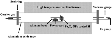 | ||
| Fig. 3 Schematic of the chemical vapor deposition system. The carrier gas is (10%) H2/Ar. The central part is the high temperature tube furnace. In the growth region, the precursor boat is 1.5 cm away from the substrate. The exhaust gas was pumped out by mechanical pump. | ||
:50 mixture of Ni and Co powder using a Nd/YAG laser with 532 nm wavelength, 10 Hz frequency and 3.5 W power.93 Wang et al. reported on the synthesis of pure single crystalline tetragonal boron nanobelt with rectangular cross-section by the laser ablation technique with a third harmonic Nd:YAG laser (wavelength = 355 nm, pulse width = 5 to 7 ns) on the target of boron pellet without using catalysts and at relatively low temperature and pressure.94 Meng et al. had successfully prepared amorphous boron nanowires by laser ablation in pressed boron targets at high temperature using the beam of a KrF excimer laser (Lambda Physik, Germany) with a wavelength of 248 nm and a pulse frequency of 10 Hz.95 Zhang and co-workers fabricated single crystalline boron nanowires on the surface of the targets by laser ablation using B/NiCo (or B/H3BO3/NiCo) target with a pulsed, frequency-doubled Nd:yttrium–aluminium–garnet (YAG) laser (wavelength, 532 nm; repetition, 10 Hz).96
3.2 Controllable growth
:50:1%) as the precursors.98 Finally, the only work on synthesis of single-walled boron nanotubes with diameters in the range of 3 nm (Fig. 4) was reported,99 a breakthrough which could open a whole new field in nanotechnology based on compound nanotubular networks.
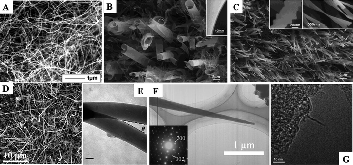 | ||
| Fig. 4 Novel boron nanostructures: (A) SEM image of amorphous boron nanowires, reproduced from ref. 70, copyright (2001) Wiley-VCH; (B), (C) SEM images of boron nanoribbons, reproduced from ref. 86, copyright (2004) American Chemical Society; (D) SEM image of single crystalline boron nanowires, reproduced from ref. 81, copyright (2008) American Institute of Physics; (E) TEM image of boron Y junction, reproduced from ref. 72, copyright (2006) American Chemical Society; (F) TEM image of boron nanocone, reproduced from ref. 79, copyright (2007) Wiley-VCH; (G) TEM image of boron nanotube, reproduced from ref. 99, copyright (2001) American Chemical Society. | ||
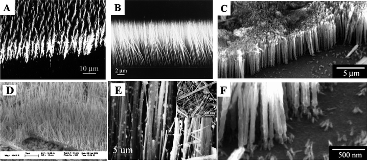 | ||
| Fig. 5 Boron nanostructure arrays: (A) feather-like armorphous boron nanowires, reproduced from ref. 88, copyright (2001) Wiley-VCH; (B) armorphous boron nanowires, reproduced from ref. 91, copyright (2002) American Institute of Physics; (C), (F) crystalline boron nanowires, reproduced from ref. 80, copyright (2008) Wiley-VCH; (D) crystalline boron nanowires, reproduced from ref. 100, copyright (2004) American Institute of Physics; (E) crystalline boron nanowires with templates, reproduced from ref. 85, copyright (2003) Elsevier Science B. V. | ||
The fabrication of patterned nanostructures for applications including nanoelectronics through display units, information storage devices, micro-optical components, and miniaturized sensors has had a great deal of interest in the past few years.101–103 To date, much effort has been focused on the synthesis and patterning of nanoparticles by lithography, using either photon, electron/ion-beams, or other high energy particles. In Gao's group we developed a very simple and direct methodology to pattern Fe3O4 nanoparticles on an Si(111) surface by the self-assembly technique. Fe3O4 nanoparticles were synthesized by a simple high temperature solution phase reaction technique.71 To realize self-assembled Fe3O4 nanoparticles on Si(111) wafer the concentration, dosage of the solution, and temperature of the substrate has been well controlled. Fe3O4 nanoparticles of uniform size have been used as a catalyst to synthesize one-dimensional 1D nanostructures.76–78 The patterned Si wafers (Fig. 6A–C) were subsequently used as substrates to grow patterned boron nanowires (Fig. 6D–I) via a simple chemical vapor deposition.82
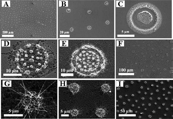 | ||
| Fig. 6 (A–C) The SEM images of assembled Fe3O4 nanoparticles on silicon substrate; (D–I) The SEM images of patterned boron nanowires grown on the substrate. Reproduced from ref. 82, copyright (2009) American Institute of Physics. | ||
4. Potential applications
4.1 Electric transport
The ordered crystal structures of boron are built on a B12 icosahedral unit and include α-rhombohedral, α-tetragonal, and β-rhombohedral units.54,84 The conductivity of bulk boron varies from 10−4 to 10−7 (Ω cm)−1 due to its crystal structure variety. The first theoretical predcation of the transport properties of boron nanostructures was carried out by P. Pandey and co-workers.57 They calculated the I–V characteristics of (6,0) and (0,6) single wall boron nanotubes (SWBNTs) using a tight-binding approach and the Landauer–Büttiker multichannel formalism. The conductivity in SWBNT is predicated to be higher than that in single wall carbon nanotubes (SWCNT) and the chirality of boron nanotubes does not appear to play a significant role in determining the I–V characteristics of a BNT. They claimed that it is attributed to a mixture of localized two-center bonds and delocalized multicenter electron-deficient nature of boron bonds in SWBNT. Following this, they also found that the differential conductance and the tunnel current for B-fullerenes sandwiched between Au contacts are much higher than those for C60, which is due to metal-like states, formed from the hybridization of Au 6s orbital with the highest occupied molecular orbital of B-fullerenes delocalized over the equator of the icosahedral cages.104 Due to their predicted enhanced electron transport properties, B nanostructures appear to be attractive candidates for future nanoscale electronics. These predictions also stimulated great interest in experimental measurement of the conductivities of 1D boron nanostructures. If the experimental results are consistent with what has been predicted, 1D boron nanostructures will be very promising as building blocks for the next generation of nanoelectronic devices.An early measurement was carried out on the boron nanowires with diameters of 46, 115, and 58 nm, however, without identifying their crystal structures. The conductivity was measured using two PtIr probe tips in the SEM,84 and it came out on the order of 10−5 (Ω cm)−1. This work was then followed by building two boron nanowire devices using Ni and Ti as contact electrodes by electron-beam lithography.105 Because boron is a p-type semiconductor, Ni electrode had a good Ohmic contact to boron nanowires, while Ti electrode had Schottky-barrier contacts. The conductivity of a single boron nanowire with an average diameter of 60 nm was measured at the order of 10−2 (Ω cm)−1 after annealed at 400 °C for 10 min. It turned out a four-fold increase over the conductivity of β-rhombohedral bulk broron. Thermal treatment led to an improvement of the interfacial contact between the electrodes and the boron nanowire.
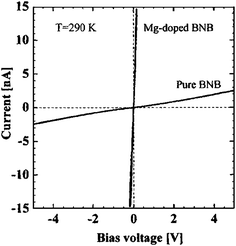
The room temperature conductivities of boron nanobelts with α-tetragonal structure were reported by Kirihara et al.106,107 It was demonstrated that the conductivities of boron nanobelts were improved to 2.5–4.5 × 10⁻³ (Ω cm)−1 by Mg doping and it was proportional to the operating temperature. The theoretical study and some experimental results suggested that the conductivity of bulk boron can be improved by appropriate carbon doping. In the unit cell of α-tetragonal boron, there are several interstitial atomic sites that can accommodate some adventitious atoms. The electronic transport of Mg-doped boron nanobelts was found to be 2.8 × 10⁻¹ (Ω cm)−1 at 290 K, which was hundred of times higher than pure boron nanobelts. The Mg atoms occupying the interstitial sites donate electrons to the densely distributed intrinsic acceptor levels in a rigid band scheme. It might lead to the high value of N(EF) (the electron density of localized state at the Fermi level) and thus improved the overall conductivity of nanobelts. This section focuses on the recent progress on experimental measurement of electric transport in single crystalline boron 1D nanostructures.
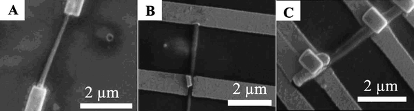 | ||
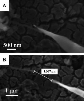
| Fig. 7 SEM images of three boron nanocone devices with different diameters and lengths connected with Au electrodes. (A) Device 1 (length, 3.1 μm, the diameters of both ends, 110 nm and 190 nm); (B) Device 2 (length, 3.8 μm, diameters of both ends, 240 nm and 280 nm); (C) Device 3 (length, 2.5 μm, diameters of both ends, 450 nm). Reproduced from ref. 79, copyright (2007) Wiley-VCH. | ||
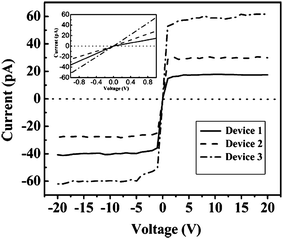 | ||
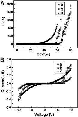
| Fig. 8 Room temperature current–voltage (I–V) curves of three devices at the voltage range of −20 V to 20 V, the inset is I–V curves at small voltage range of −1.0 V to 1.0 V. Reproduced from ref. 79, copyright (2007) Wiley-VCH. | ||
Device 3 with comparative diameter size of both ends has the similar I–V curve shape with that of boron nanowires. The velocity excursion of carriers of boron nanocones for Device 1 and 2 is different at the same positive and negative potentials due to the diameter size distinctness along the cones, which results in the variety of carrier mobilities and thus led to the different saturation currents.
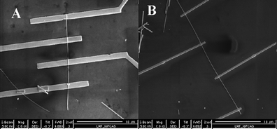 | ||
| Fig. 9 Typical SEM images of a boron nanowire device made by electron beam lithography (EBL) (A) and a nanowire device fabricated by focused ion beam (FIB) (B). | ||
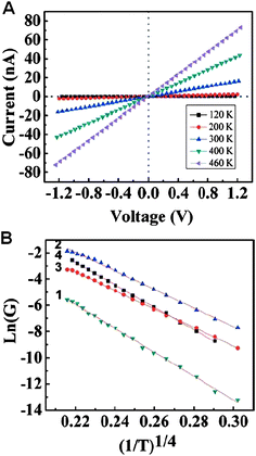 | ||
| Fig. 10 (A) The I–V characterization of a boron nanowire. (B) Temperature dependence of electrical conductivities of four different devices. The indexed numbers of each curve represent the corresponding devices. Reproduced from ref. 81, copyright (2008) American Institute of Physics. | ||
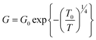
Fig. 10B gives linear relationships between Ln(G) and (1/T)1/4 of these four devices. Here, G is the conductivity and T is the temperature. Such linear dependence fits in with Mott's variable range hopping (VRH) model, assuming that the carrier transport occurs by thermal activation process between the localized states. According to Mott's law of three-dimensional VRH, the conductivity G can be expressed as,
 | (1) |
 | (2) |
| Samples | β-Rhombohedral B (polycrystalline) | β-Rhombohedral B (single crystal) | Device 1 | Device 2 | Device 3 | Device 4 |
|---|---|---|---|---|---|---|
| T o/K | 5.1 × 10⁹ | 8.7 × 10⁷ | 6.8 × 10⁷ | 2.56 × 10⁷ | 2.47 × 10⁷ | 5.4 × 10⁷ |
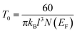
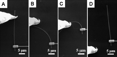
It is interesting that the conductance of single crystal boron nanowires is very robust even under large strain. In the experiment, one end of an individual boron nanowire was fixed by a Pt electrode through focused ion beam operation. One Au tip in the four-probe STM system was used as an electrode in a two-terminal configuration as well as the nanowire manipulator. As illustrated in Fig. 11, the electrical conductance measurement was monitored during the process of bending the nanowire.81 The mechanical strain the nanowire experienced can be quantized as ε = r/R, where r and R represent the nanowire's radius and the radius of curvature, respectively. The nanowire remains intact even after 3% strain bending and manifests excellent resilience (Fig. 11C). The conductivity of boron nanowire persisted while increasing the strain gradually. The measured resistivities for each step in Fig. 11A–C are 139.3, 143.8, and 142.4 Ω cm, respectively. After plotting the data of ln(G) versus (1/T)1/4 with and without mechanical strain (Fig. 12), it was found that the electrical conductivity is independent on mechanical strain. It is similar to the one without mechanical strain. It indicates that the strain applied on the boron nanowire did not change the electron density of localized states at the Fermi level. This finding demonstrated that the single crystalline boron nanowires are very promising as building blocks for flexible nanoelectronic devices.
 | ||
| Fig. 11 SEM images of a single boron nanowire under a mechanical bending process. Reproduced from ref. 81, copyright (2008) American Institute of Physics. | ||
 | ||
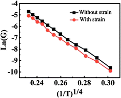
| Fig. 13 SEM images of boron nanowires after Ni/Au electrode fabrication. (A) A pure boron nanowire; and (B) a Mg-doped boron nanowire. Scale bar is 2 μm. Reproduced from ref. 107, copyright (2005) American Vacuum Society. | ||
4.2 Field emssion
Metal or semiconductor 1D nanostructures such as nanotubes and nanowires have been well accepted as ideal field emission electron sources for emitting electrons at low electric field due to their nanoscale and special geometry (high aspect ratio and lower curvature radius).43,112,113 A good emitter material for field emission requires not only a low turn-on voltage, but also a high durable emission current. It needs some properties, such as small electron affinity, low work function, high aspect ratio, high thermal stability and better mechanical strength at high temperature. In the past decade, a lot of materials including Spindt-tip arrays,114 low electron affinity III–V nitride nanocones/nanowires,115,116 diamond films,117 transition metal oxide nanowires,118–121 and carbon nanotubes122–124 have been systemically studied as field emitters. Among these nanostructures, carbon nanotubes were well-recognized as one of best field emission materials. However, due to their poor emission stability and low melting point, carbon nanotubes are limited in building field emission devices. This section reviews the field emission properties of single crystalline boron 1D nanostructures. Compared to other materials, the nature of boron offers its 1D nanostructures many advantages, such as a high melting point ensuring long-term stability, low-electron-affinity-induced large-field emission current density, and strong mechanical strength, resulting in high mechanical performance.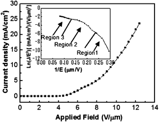
 | ||
| Fig. 16 SEM images of the single boron nanowire during FE measurements. SEM images of the W probe and the single nanowire (A) before and (B) during the measurement. Reproduced from ref. 80, copyright (2005) Wiley-VCH. | ||
 | ||
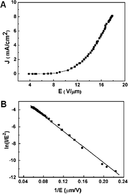
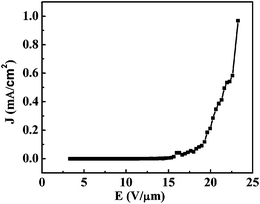
| Fig. 17 (A) The current-electric field (I–E) curves of individual boron nanowires: a–c refer to the three different boron nanowires. (B) The corresponding current–voltage (I–V) curves of these three individual boron nanowires (a–c) in FE measurements. Reproduced from ref. 80, copyright (2005) Wiley-VCH. | ||
It is noticed that these three representative field emission behaviors exhibited slight differences. Nanowire a showed the best behavior although there was no remarkbale morphology difference among the three nanowires. To explore the details of field emission behavior, the conductivity of these three typical nanowires was also measured and plotted in Fig. 17B. Through this measurement, it was found that the three nanowires process different electrical conductivities. Nanowire a and c showed the highest (8 × 10⁻³ (Ω cm)−1) and the lowest (3.2 × 10⁻³ (Ω cm)−1) conductivities, respectively. It is probably the difference in conductivity that results in the difference in field emission behavior. These results suggested that the field emission performance of an individual boron nanowire seems proportional to its electrical conductance. The measured field emission featured a behavior up to 4 μA without breaking down, which is very encouraging compared to the best results obtained from other nanowires.125–127
Conclusions and outlook
Recent advances in the dynamic area of boron nanostructures have been drafted in this review paper. Recently, various 1D boron nanomaterials, such as nanowires, nanobelts, nanocones and nanotubes have been successfully synthesized by chemical and physical methods. We classified these methods into three categories: 1) chemical vapor deposition (CVD) with gas or solid precursors; 2) magnetron sputtering; and 3) laser ablation. Several technical approaches for fabricating high density boron 1D nanostructure arrays and patterned nanostructures were also discussed. Although significant progress has been made on controlled growth of 1D boron nanostructures, a breakthrough in terms of highly ordered arrays, large scale synthesis, patterned growth, morphology control as well as simplifying current recipes is still highly desired. In particular, the controlled synthesis of boron nanotubes currently is a focus area to be developed since the theoretical studies have predicted a high electric conductivity of boron nanotubes, which are promising to exhibit even higher electric conductivity than carbon nanotubes.56,58 To date, only one attempt was successful on the synthesis of boron nanotubes by employing Mg-MCM-41 as template99 and the progress on high quality, large scale or highly crystalline boron nanotubes as well as the transport measurements on these novel structures remained blank in this field. More efforts from the experimental community are still required to develop new methods not only to synthesis novel nanostructures (such as nanotubes and fullerenes) but also to run measurements on the conductivity of these nanostructures. To verify these theoretical predictions of boron nanostructures experimentally is not only fundamentally interesting, but also appealing for the discovery of new generation nanodevices.The two main physical properties of 1D boron nanostructures are electronic transport and field emission, which are quite interesting as they give 1D boron nanostructures great potential for field emission, flexible displays, superconductors, energy storage, and nanoelectronic devices. However, like most popular 1D nanomaterials, there are still many key scientific problems to be understood for their true application. One aspect is the relationship between the transport properties and crystal structures of boron. Boron has several different crystal structures. It is important to study the transport properties of boron nanostructures with different crystal structures. Moreover, more effort should be devoted to understand the transport mechanism by varying the measurement conditions, such as temperature, strain, and doping. For field emission applications, more attention may be paid to both synthesis techniques and property measurements. Boron nanostructures with uniform size, proper density, and/or a controlled interval distance are highly essential to enhance the properties of field emission. In addition, to realize flexible displays, flexible and conductive substrates for growing boron nanostructures are also highly desired.
There are almost unlimited research opportunities that are being and will be explored by researchers in this dynamic area. By understanding these scientific and technical issues, we believe that 1D boron nanostructures will continue to give exciting results toward their application.
Acknowledgements
The work is supported by National High Technology Program of China (863 Program, Grant No. 2007AA03Z305), National Basic Research Program of China (973 Program, Grant No. 2007CB935500) and National Natural Science Foundation of China (Grant No. 50872147, U0734003).Notes and references
- Y. Xia, P. Yang, Y. Sun, Y. Wu, B. Mayers, B. Gates, Y. Yin, F. Kim and H. Yan, Adv. Mater., 2003, 15, 353 CrossRef CAS.
- P. Alivisatos, Pure Appl. Chem., 2000, 72, 3 CrossRef.
- M. Nirmal and L. Brus, Acc. Chem. Res., 1999, 32, 407 CrossRef CAS.
- H. Pettersson, L. Baath, N. Carlsson, W. Seifert and L. Samuelson, Appl. Phys. Lett., 2001, 79, 78 CrossRef CAS.
- V. I. Klimov, A. A. Mikhailovsky, S. Xu, A. Malko, J. A. Hollingsworth, C. A. Leatherdale, H. J. Eisler and M. G. Bawendi, Science, 2000, 314, 290.
- J. Phillips, J. Appl. Phys., 2002, 91, 4590 CrossRef.
- D. L. Klein, R. Roth, A. K. L. Lim, A. P. Alivisatos and P. L. McEuen, Nature, 1997, 389, 699 CrossRef CAS.
- H. Sakaki, Jpn. J. Appl. Phys., 1980, 19, L735 CrossRef CAS.
- Z. G. Wu, J. B. Neaton and J. C. Grossman, Phys. Rev. Lett., 2008, 100, 246804 CrossRef.
- G. Hodes, Adv. Mater., 2007, 19, 639 CrossRef CAS.
- Q. Zhu, K. F. Karlsson, E. Pelucchi and E. Kapon, Nano Lett., 2007, 7, 2227 CrossRef CAS.
- Z. (J.) Xu, M. Lu, X. Guo and H. Lin, J. Mol. Catal. A: Chem., 2005, 226, 123 CrossRef CAS.
- G. Che, B. B. Lakshmi, C. R. Martin and E. R. Fisher, Langmuir, 1999, 15, 750 CrossRef CAS.
- N. Wang, Y. Cai and R. Q. Zhang, Mater. Sci. Eng., R, 2008, 60, 1–51 CrossRef.
- C. M. Lieber and Z. L. Wang, MRS Bull., 2007, 32, 99–108 CAS.
- F. Liu, P. J. Cao, H. R. Zhang, C. M. Shen, J. Q. Li and H.-J. Gao, J. Cryst. Growth, 2005, 274, 126–131 CrossRef CAS.
- Z. W. Pan, Z. R. Dai and Z. L. Wang, Science, 2001, 291, 1947 CrossRef CAS.
- C. Li, D. H. Zhang, S. Han, X. L. Liu, T. Tang and C. W. Zhou, Adv. Mater., 2003, 15, 143 CrossRef CAS.
- Z. R. Dai, J. L. Gole, J. D. Stout and Z. L. Wang, J. Phys. Chem. B, 2002, 106, 1274 CrossRef CAS.
- M. S. Dresselhaus, G. Dresselhaus, and P. Avouris, Carbon Nanotubes: Synthesis, Structure, and Application, Springer, New York, 2001 Search PubMed.
- T. Guo, P. Nokolaev, A. Thess, D. T. Colbert and R. E. Smalley, Chem. Phys. Lett., 1995, 243, 49 CrossRef CAS.
- S. S. Fan, M. G. Chapline, N. R. Franklin, T. W. Tombler, A. M. Cassell and H. J. Dai, Science, 1999, 283, 512 CrossRef CAS.
- A. M. Morales and C. M. Lieber, Science, 1998, 279, 208 CrossRef CAS.
- D. Wang and H. Dai, Appl. Phys. A: Mater. Sci. Process., 2006, 85, 217 CrossRef CAS.
- S. A. Dayeh, E. T. Yu and D. L. Wang, J. Phys. Chem. C, 2007, 111, 13331 CrossRef CAS.
- C. Liu, Z. Hu, Q. Wu, X. Z. Wang, Y. Chen, H. Sang, J. M. Zhu, S. Z. Deng and N. S. Xu, J. Am. Chem. Soc., 2005, 127, 1318 CrossRef CAS.
- N. G. Chopra, R. J. Luyken, K. Cherrey, V. H. Crespi, M. L. Cohen, S. G. Louie and A. Zettl, Science, 1995, 269, 966 CrossRef CAS.
- D. V. Talapin, E. V. Shevchenko, C. B. Murray, A. Kornowski, S. Förster and H. Weller, J. Am. Chem. Soc., 2004, 126, 12984 CrossRef CAS.
- C. M. Shen, X. G. Zhang and H. L. Li, Mater. Sci. Eng., A, 2001, 303, 19 CrossRef.
- Y. Jiang, X. M. Meng, W. C. Yiu, J. Liu, J. X. Ding, C. S. Lee and S. T. Lee, J. Phys. Chem. B, 2004, 108, 2784 CrossRef CAS.
- R. H. Baughman, A. A. Zakhidov and W. A. de Heer, Science, 2002, 297, 787 CrossRef CAS.
- D. R. Kauffman and A. Star, Small, 2007, 3, 1324 CrossRef CAS.
- Z. Y. Fan, D. W. Wang, P. C. Chang, W. Y. Tseng and J. G. Lu, Appl. Phys. Lett., 2004, 85, 5923 CrossRef CAS.
- X. D. Wang, J. H. Song, J. Liu and Z. L. Wang, Science, 2007, 316, 102 CrossRef CAS.
- X. F. Duan, Y. Huang, Y. Cui, J. F. Wang and C. M. Lieber, Nature, 2001, 409, 66–69 CrossRef CAS.
- J. M. Bao, M. A. Zimmler and F. Capasso, Nano Lett., 2006, 6, 1719 CrossRef CAS.
- F. Qian, S. Gradečak, Y. Li, C. Y. Wen and C. M. Lieber, Nano Lett., 2005, 5, 2287 CrossRef CAS.
- A. M. Rao, X. H. Ji and Terry M. Tritt, MRS Bull., 2006, 31, 218 CAS.
- A. I. Hochbaum, R. K. Chen, R. D. Delgado, W. J. Liang, E. C. Garnett, M. Najarian, A. Majumdar and P. D. Yang, Nature, 2008, 451, 163 CrossRef CAS.
- A. I. Boukai, Y. Bunimovich, J. Tahir-Kheli, J. K. Yu, W. A. Goddard and J. R. Heath, Nature, 2008, 451, 168 CrossRef CAS.
- Y. Huang and C. M. Lieber, Pure Appl. Chem., 2004, 76, 2051 CrossRef CAS.
- W. A. de Heer, A. Chatelain and D. Ugarte, Science, 1995, 270, 1179 CrossRef CAS.
- W. I. Milne, K. B. K. Teo, G. A. J. Amaratunga, P. Legagneux, L. Gangloff, J.-P. Schnell, V. Semet, V. T. Binh and O. Groening, J. Mater. Chem., 2004, 14, 933 RSC.
- N. S. Xu and S. Ejaz, Mater. Sci. Eng., R, 2005, 48, 47 CrossRef.
- J. Zhou, L. Gong, S. Z. Deng, J. Chen, J. C. She, N. S. Xu, R. Yang and Z. Wang, Appl. Phys. Lett., 2005, 87, 223108 CrossRef.
- Z. Y. Fan, D. W. Wang, P. C. Chang, W. Y. Tseng and J. G. Lu, Appl. Phys. Lett., 2004, 85, 5923 CrossRef CAS.
- Q. Wan and T. H. Wang, Chem. Commun., 2005, 3841 RSC.
- X. F. Chu, C. H. Wang, D. L. Jiang and C. M. Zheng, Chem. Phys. Lett., 2004, 399, 461 CrossRef CAS.
- N. N. Greenwood and A. Earnshaw, Chemistry of the Elements, Butterworth-Heinemann, Oxford, 1998 Search PubMed.
- G. V. Tsagareishvili and F. N. Tavadze, Prog. Cryst. Growth Charact. Mater., 1988, 16, 341 CrossRef CAS.
- D. Emin, Phys. Today, 1987, 40, 55 CrossRef CAS.
- G. K. Gaule, Boron: Preparation, Properties, and Application, Plenum, New York, 1965 Search PubMed.
- D. G. Hinks, H. Claus and J. D. Jorgensen, Nature, 2001, 411, 457 CrossRef CAS.
- A. Ulas, K. K. Kuo and C. Gotzmer, Combust. Flame, 2001, 127, 1935 CrossRef CAS.
- I. Boustani and A. Quandt, Europhys. Lett., 1997, 39, 527 CrossRef CAS.
- I. Boustani, A. Quandt, E. Hernández and A. Rubio, J. Chem. Phys., 1999, 110, 3176 CrossRef CAS.
- K. C. Lau, R. Pandey, R. Pati and S. P. Karna, Appl. Phys. Lett., 2006, 88, 212111 CrossRef.
- J. Kunstmann and A. Quandt, Chem. Phys. Lett., 2005, 402, 21 CrossRef CAS.
- I. Boustani, Surf. Sci., 1997, 370, 355 CrossRef CAS.
- I. Boustani, Phys. Rev. B: Condens. Matter, 1997, 55, 16426 CrossRef CAS.
- S. Chacko, D. G. Kanhere and I. Boustani, Phys. Rev. B: Condens. Matter Mater. Phys., 2003, 68, 035414 CrossRef.
- M. Fujimori, T. Nakata, T. Nakayama, E. Nishibori, K. Kimura, M. Takata and M. Sakata, Phys. Rev. Lett., 1999, 82, 4452 CrossRef CAS.
- L. Pauling, Nature of the Chemical Bond, Cornell University Press, Ithaca, 1960 Search PubMed.
- H. J. Zhai, B. Kiran, J. Li and L. S. Wang, Nat. Mater., 2003, 2, 827 CrossRef CAS.
- A. Quandt and I. Boustani, ChemPhysChem, 2005, 6, 2001 CrossRef CAS.
- A. Gindulytė, W. N. Lipscomb and L. Massa, Inorg. Chem., 1998, 37, 6544 CrossRef CAS.
- H. Tang and S. Ismail-Beigi, Phys. Rev. Lett., 2007, 99, 115501 CrossRef.
- J. Miller, Phys. Today, 2007, 20.
- X. B. Yang, Y. Ding and J. Ni, Phys. Rev. B: Condens. Matter Mater. Phys., 2008, 77, 041402 CrossRef.
- Y. Y. Wu, B. Messer and P. D. Yang, Adv. Mater., 2001, 13, 1487 CrossRef CAS.
- S. H. Yun, J. Z. Wu, A. Dias, X. Gao and U. O. Karlsson, Appl. Phys. Lett., 2005, 87, 113109 CrossRef.
- S. H. Yun, J. Z. Wu, A. Dibos, X. D. Zou and U. O. Karlsson, Nano Lett., 2006, 6, 385 CrossRef CAS.
- P. J. Cao, H. W. Liu, F. Shen, Y. G. Wang and H.-J. Gao, J. Mater. Res., 2003, 18, 1686 CrossRef CAS.
- F. Liu, P. J. Cao, H. R. Zhang, J. Q. Li and H.-J. Gao, Nanotechnology, 2004, 15, 949 CrossRef CAS.
- F. Liu, P. J. Cao, H. R. Zhang, C. M. Shen, J. Q. Li and H.-J. Gao, J. Cryst. Growth, 2005, 274, 126 CrossRef CAS.
- F. Liu, P. J. Cao, H. R. Zhang, J. F. Tian, C. W. Xiao, C. M. Shen, J. Q. Li and H.-J. Gao, Adv. Mater., 2005, 17, 1893 CrossRef CAS.
- J. F. Tian, F. Liu, C. M. Shen, L. H. Bao, X. J. Wang, D. T. Liu, H. Li, X. J. Huang, L. Q. Chen and H.-J. Gao, J. Mater. Res., 2007, 22, 1921 CrossRef CAS.
- J. F. Tian, X. J. Wang, L. H. Bao, C. Hui, F. Liu, T. Z. Yang, C. M. Shen and H.-J. Gao, Cryst. Growth Des., 2008, 8, 3160 CrossRef CAS.
- X. J. Wang, J. F. Tian, T. Z. Yang, L. H. Bao, C. Hui, F. Liu, C. M. Shen, N.S. Xu and H.-J. Gao, Adv. Mater., 2007, 19, 4480 CrossRef CAS.
- F. Liu, J. F. Tian, L. H. Bao, T. Z. Yang, C. M. Shen, X. Y. Lai, Z. M. Xiao, W.G. Xie, S. Z. Deng, J. Chen, J. C. She, N. S. Xu and H.-J. Gao, Adv. Mater., 2008, 20, 2609 CrossRef CAS.
- J. F. Tian, J. M. Cai, C. Hui, C. D. Zhang, L. H. Bao, M. Gao, C. M. Shen and H.-J. Gao, Appl. Phys. Lett., 2008, 93, 122105 CrossRef.
- J. F. Tian, C. Hui, L. H. Bao, C. Li, Y. Tian, H. Ding, C. M. Shen and H.-J. Gao, Appl. Phys. Lett., 2009, 94, 083101 CrossRef.
- T. Z. Yang, C. M. Shen, Z. A. Li, H. R. Zhang, C. W. Xiao, S. T. Chen, Z. C. Xu, D. X. Shi, J. Q. Li and H.-J. Gao, J. Phys. Chem. B, 2005, 109, 23233 CrossRef CAS.
- C. J. Otten, O. R. Loune, M. F. Yu, J. M. Cowley, M. J. Dyer, R. S. Ruoff and W. E. Buhro, J. Am. Chem. Soc., 2002, 124, 4564 CrossRef CAS.
- Q. Yang, J. Sha, J. Xu, Y. J. Ji, X. Y. Ma, J. J. Niu, H. Q. Hua and D. R. Yang, Chem. Phys. Lett., 2003, 379, 87 CrossRef CAS.
- T. T. Xu, J. G. Zheng, N. Q. Wu, A. W. Nicholls, J. R. Roth, D. A. Dikin and R. S. Ruoff, Nano Lett., 2004, 4, 963 CrossRef CAS.
- L. Guo, R. N. Singh and H. -J. Kleebe, Chem. Vap. Deposition, 2006, 12, 448 CrossRef CAS.
- L. M. Cao, Z. Zhang, L. L. Sun, M. He, Y. Q. Wang, Y. C. Li, X. Y. Zhang, G. Li, J. Zhang and W. K. Wang, Adv. Mater., 2001, 13, 1701 CrossRef CAS; Y. Q. Wang, X. F. Duan, L. M. Cao and W. K. Wang, Chem. Phys. Lett., 2002, 359, 273 CrossRef CAS.
- L. M. Cao, K. Hahn, Y. Q. Wang, C. Scheu, Z. Zhang, C. X. Gao, Y. C. Li, X. Y. Zhang, L. L. Sun and W. K. Wang, Adv. Mater., 2002, 14, 1294 CrossRef CAS.
- Y. Q. Wang, L. M. Cao and X. F. duan, Chem. Phys. Lett., 2003, 367, 495–499 CrossRef CAS.
- L. M. Cao, K. Hahn, M. Ruhle, C. Scheu, Y. Q. Wang, Z. Zhang, C. X. Gao, Y. C. Li, X. Y. Zhang, M. He, L. L. Sun and W. K. Wang, Appl. Phys. Lett., 2002, 80, 4226 CrossRef CAS.
- Y. P. Gao, Z. Xu and R. P. Liu, Mater. Sci. Eng., A, 2006, 434, 53 CrossRef.
- Y. J. Zhang, H. Ago, M. Yumura, T. Komatsu, S. Ohshima, K. Uchida and S. Iijima, Chem. Commun., 2002, 2806 RSC.
- Z. K. Wang, Y. Shimizu, T. Sasaki, K. Kawaguchi, K. Kimura and N. Koshizaki, Chem. Phys. Lett., 2003, 368, 663 CrossRef CAS; Z. Wang, T. Sasaki, Y. Shimizu, K. Kirihara, K. Kawaguchi, K. Kimura and N. Koshizaki, Appl. Phys. A: Mater. Sci. Process., 2004, 79, 891 CAS.
- X. M. Meng, J. Q. Hu, Y. Jiang, C. S. Lee and S. T. Lee, Chem. Phys. Lett., 2003, 370, 825 CrossRef CAS.
- Y. J. Zhang, H. Ago, M. Yumura, S. Ohshima, K. Uchida, T. Komatsu and S. Iijima, Chem. Phys. Lett., 2004, 385, 177 CrossRef CAS.
- Y. Q. Wang and X. F. Duan, Appl. Phys. Lett., 2003, 82, 272 CrossRef CAS.
- Q. Yang, J. Sha, L. Wang, Z. Xu, X. Ma, J. Wang and D. Yang, J. Mater. Sci., 2006, 41, 3547 CrossRef CAS.
- D. Ciuparu, R. F. Klie, Y. Zhu and L. Pfefferle, J. Phys. Chem. B, 2004, 108, 3867.
- S. H. Yun, A. Dibos, J. Z. Wu and D. K. Kim, Appl. Phys. Lett., 2004, 84, 2892 CrossRef CAS.
- S. M. Sze, Semiconductor Devices: Physics and Technology, Wiley, New York, 1985 Search PubMed.
- W. Menz, J. Mohr and O. Paul, Microsystem Technology, 2nd edn, Wiley-VCH, Weinheim, 2001 Search PubMed.
- M. Geissler and Y. Xia, Adv. Mater., 2004, 16, 1249 CrossRef CAS.
- H. He, R. Pandey, I. Boustani and S. P. Karna, J. Phys. Chem. C, 2010, 114, 4149 CrossRef CAS.
- D. W. Wang, J. G. Lu, C. Jones Otten and W. E. Buhro, Appl. Phys. Lett., 2003, 83, 5280 CrossRef CAS.
- K. Kirihara, Z. Wang, K. Kawaguchi, Y. Shimizu, T. Sasaki, N. Koshizaki, K. Soga and K. Kimura, Appl. Phys. Lett., 2005, 86, 212101 CrossRef.
- K. Kirihara, Z. Wang, K. Kawaguchi, Y. Shimizu, T. Sasaki, N. Koshizaki, H. Hyodo, K. Soga and K. Kimura, J. Vac. Sci. Technol., B, 2005, 23, 2510 CrossRef CAS.
- K. H. Hellwege, Landolt–Bornstein Numerical Data and Functional Relationships, in Science and Technology, Springer, Berlin 1983 Search PubMed.
- D. Femandez-Hevia, J. de Frutos, A. C. Cabalero and J. F. Fernandez, Appl. Phys. Lett., 2003, 82, 212 CrossRef.
- Q. H. Li, Q. Wan, Y. G. Wang and T. H. Wang, Appl. Phys. Lett., 2005, 86, 263101 CrossRef.
- J. Nagamatsu, N. Nakagawa, T. Muranaka, Y. Zenitani and J. Akimitsu, Nature, 2001, 410, 63 CrossRef CAS.
- H. J. Dai, Acc. Chem. Res., 2002, 35, 1035 CrossRef CAS.
- X. S. Fang, Y. Bando, U. K. Gautam, C. H. Ye and D. Golberg, J. Mater. Chem., 2008, 18, 509 RSC.
- A. A. Talin, K. A. Dean and J. E. Jaslie, Solid-State Electron., 2001, 45, 963 CrossRef CAS.
- Q. Zhao, J. Xu, X. Y. Xu, Z. Wang and D. P. Yu, Appl. Phys. Lett., 2004, 85, 5331 CrossRef CAS.
- S. C. Shi, C. F. Chen, St. Chattopadhyay, K. H. Chen and L. C. Chen, Appl. Phys. Lett., 2005, 87, 073109 CrossRef.
- M. W. Geis, J. C. Twicell, J. Macaulay and K. Okana, Appl. Phys. Lett., 1995, 67, 1328 CrossRef CAS.
- Y. B. Li, Y. Bando and D. Golberg, Appl. Phys. Lett., 2004, 84, 3603 CrossRef CAS.
- W. Z. Wang, B. Q. Zeng, J. Yang, B. Poudel, J. Y. Huang, M. J. Naughton and Z. F. Ren, Adv. Mater., 2006, 18, 3275 CrossRef CAS.
- G. C. Yi, C. R. Wang and W. Il Park, Semicond. Sci. Technol., 2005, 20, S22 CrossRef CAS.
- J. Chen, Y. Y. Dai, J. Luo, Z. L. Li, S. Z. Deng, J. C. She and N. S. Xu, Appl. Phys. Lett., 2007, 90, 253105 CrossRef.
- J. M. Bonard, N. Weiss, H. Kind, T. Stöckli, L. Forró, K. Kern and A. Châtelain, Adv. Mater., 2001, 13, 184 CrossRef CAS.
- S. D. Liang and N. S. Xu, Appl. Phys. Lett., 2003, 83, 1213 CrossRef CAS.
- P. Yaghoobi and A. Nojeh, Mod. Phys. Lett. B, 2007, 21, 1807 CrossRef CAS.
- H. Zhang, J. Tang, Q. Zhang, G. Zhao, G. Yang, J. Zhang, O. Zhou and L.-C. Qin, Adv. Mater., 2006, 18, 87 CrossRef CAS.
- N. S. Ramgir, I. S. Mulla, K. Vijayamohanan, D. J. Late, A. B. Bhise, M. A. More and D. S. Joag, Appl. Phys. Lett., 2006, 88, 107.
- Y. Yu, C. H. Jin, R. H. Wang, Q. Chen and L.-M. Peng, J. Phys. Chem. B, 2005, 109, 772.
- M. Rao, D. Jacques, R. C. Haddon, W. Zhu, C. Bower and S. Jin, Appl. Phys. Lett., 2000, 76, 3813 CrossRef CAS.
- Y. B. Li, Y. Bando and D. Golberg, Adv. Mater., 2003, 15, 1294 CrossRef CAS.
- J.-M. Bonard, K. A. Dean, B. F. Coll and C. Klinke, Phys. Rev. Lett., 2002, 89(197), 602.
- L. Nilsson, O. Groening, C. Emmenegger, O. Kuettel, E. Schaller, L. Schlapbach, H. Kind, J.-M. Bonard and K. Kern, Appl. Phys. Lett., 2000, 76, 2071 CrossRef CAS.
- J.-M. Bonard, N. Weiss, H. Kind, T. Stoöckli, L. Forroó, K. Kern and A. Chatelain, Adv. Mater., 2001, 13, 184 CrossRef CAS.
- L. Nilsson, O. Groening, P. Groening, O. Kuettel and L. Schlapbach, J. Appl. Phys., 2001, 90, 768 CrossRef CAS.
- C. Liu, Z. Hu, Q. Wu, X. Z. Wang, Y. Chen, H. Sang, J. M. Zhu, S. Z. Deng and N. S. Xu, J. Am. Chem. Soc., 2005, 127, 1318 CrossRef CAS.
- K. H. Chen, J. J. Wu, L. C. Chen, C. Y. Wen, P. D. Kichambare, F. G. Tarntair, P. F. Kuo, S. W. Chang and Y. F. Chen, Diamond Relat. Mater., 2000, 9, 124.
- F. G. Tarntair, C. Y. Wen, L. C. Chen, J. J. Wu, K. H. Chen, P. F. Kuo, S. W. Chang, Y. F. Chen, W. K. Hong and H. C. Cheng, Appl. Phys. Lett., 2000, 76, 2630 CrossRef CAS.
- K. W. Wong, X. T. Zhou, F. C. K. Au, H. L. Lai, C. S. Lee and S. T. Lee, Appl. Phys. Lett., 1999, 75, 2918 CrossRef CAS.
| This journal is © The Royal Society of Chemistry 2010 |