DOI:
10.1039/B9NR00415G
(Review Article)
Nanoscale, 2010,
2, 168-187
One-dimensional CdSnanostructures: synthesis, properties, and applications
Received
(in Hong Kong, China)
17th December 2009
, Accepted 13th January 2010
First published on 25th January 2010
Abstract
One-dimensional (1D) semiconductor nanostructures are of prime interest due to their potential in investigating the size and dimensionality dependence of the materials' physical properties and constructing nanoscale electronic and optoelectronic devices. Cadmium sulfide (CdS) is an important semiconductor compound of the II–VI group, and its synthesis and properties have been of growing interest owing to prominent applications in several fields. This article provides a comprehensive review of the state-of-the-art research activities that focus on the rational synthesis, novel properties and unique applications of 1D CdSnanostructures in nanotechnology. It begins with the rational design and synthesis of 1D CdSnanostructures, and then highlights a range of unique properties and applications (e.g. photoluminescence, cathodoluminescence, electrochemiluminescence, photocatalysis, lasers, waveguides, modulators, solar cells, field-effect transistors, photodetectors, field-emitters, and nanogenerators) associated with them. Finally, the review is concluded with the author outlook of the perspectives with respect to future research on 1D CdSnanostructures.
 Tianyou Zhai | Tianyou Zhai was born in Henan, China, in 1980. He received a BSc degree in chemistry from Zhengzhou University in 2003, and then received a PhD degree in physical chemistry from the Institute of Chemistry, Chinese Academy of Sciences (ICCAS) under the supervision of Prof. Jiannian Yao and Ying Ma in 2008. Currently, he is a JSPS postdoctoral fellow of Prof. Yoshio Bando's group at the National Institute for Materials Science (NIMS). He has authored and co-authored over 30 refereed journal publications. His research interests include the controlled fabrication and characterization of 1D nanostructures and their device applications in electronics and optoelectronics. He is a member of the Editorial Advisory Board of several international journals. He received the Special Young Scientist Prize of ICCAS in 2006, 2007 and the P&G Excellent Doctoral Scholarship of CAS in 2008. |
 Xiaosheng Fang | Xiaosheng Fang obtained his PhD degree from Institute of Solid State Physics, Chinese Academy of Sciences in 2006 under the supervision of Prof. Lide Zhang. After that he joined Prof. Yoshio Bando's group as a JSPS postdoctoral fellow. Currently, he is an International Center for Young Scientists (ICYS)-International Center for Materials Nanoarchitectonics (MANA) researcher within NIMS. He has authored and co-authored 56 refereed journal publications, 10 review papers, an English monograph, and four book chapters. His publications have been cited over 1350 times. His current research topic is the controlled fabrication, novel properties and optoelectronic applications of 1D nanostructures, with a special focus on ZnS nanostructure-based optoelectronic sensors. He is a member of the Editorial Advisory Board of several international journals. He received a Special Prize of President Scholarship of Chinese Academy of Sciences 2006 and a Thomson Reuters Research Front Award in 2008. |
 Liang Li | Liang Li was born in Anhui province, China, in 1979. He joined Prof. Guanghai Li's group in 2001 and obtained his PhD degree in nanostructure materials from the Chinese Academy of Sciences. He was awarded the Excellent President Scholarship in 2006. After a postdoctoral fellowship at the National University of Singapore (NUS), he worked within Prof. Naoto Koshizaki's group as a JSPS fellow in the National Institute of Advanced Industrial Science and Technology (AIST) from 2007 to 2009, and is now in Prof. Yoshio Bando's group at the National Institute of Materials Science (NIMS) in Japan as a MANA postdoctoral fellow. During these terms he mainly studied the fabrication of nanostructures by PLD, CVD, and electrochemical deposition combined with various templates, such as porous alumina membranes and polystyrene colloid spheres. He also analyzed electronic transport, gas sensing, and field-emission in nanostructures. He has authored and co-authored about 45 refereed publications since 2003, which have generated over 450 citations. |
 Yoshio Bando | Yoshio Bando received his PhD degree from Osaka University in 1975 and joined the National Institute for Research in Inorganic Materials (at present NIMS) in the same year. From 1979 to 1981 he worked as a visiting researcher at Arizona State University. Currently, he is a Chief Operating Officer (COO) of the International Center for Materials Nanoarchitectonics (MANA) and a Fellow within the National Institute for Materials Science (NIMS). He is also a visiting Professor at both Waseda University and the University of Tokyo. His current research concentrates on the synthesis and properties of various inorganic nanostructures and their TEM characterizations. He has published more than 450 papers in international journals and the total number of citations of his papers is over 11![[hair space]](https://www.rsc.org/images/entities/char_200a.gif) 000. The H-index of his publications is 57. He also holds more than 150 patents. He received the 16th Tsukuba Prize in 2005 for his studies on novel inorganic nanotubes and nanothermometers. 000. The H-index of his publications is 57. He also holds more than 150 patents. He received the 16th Tsukuba Prize in 2005 for his studies on novel inorganic nanotubes and nanothermometers. |
 Dmitri Golberg | Dmitri Golberg obtained his PhD degree from the Central Research Institute for Ferrous Metallurgy, Moscow, Russia, in 1990, and joined the National Institute for Materials Science (NIMS), Tsukuba, Japan, five years later. To date, he has authored and co-authored more than 350 original papers and nearly 100 patents. His papers have been cited over 6300 times. The H-index of his publications is 42. In 2005 he was awarded the 16th Tsukuba Prize for his studies on inorganic nanotubes using electron microscopy. He is currently a Group Leader and Principal Investigator within the WPI International Center for Materials Nanoarchitectonics (MANA) of NIMS, and an Associate Professor of the University of Tsukuba. His current research focuses on nanoscale material electrical and mechanical property studies in a transmission electron microscope. |
1. Introduction
One-dimensional (1D) nanostructures such as nanowires, nanobelts, and nanotubes have stimulated an increasing interest due to their importance in basic scientific research and potential technological applications.1–6 It is generally accepted that 1D nanostructures are ideal systems for exploring a large number of novel phenomena at the nanoscale and investigating the size and dimensionality dependence of functional properties. They are also expected to play important roles as both interconnects and the key units in nanoscale electronic, optoelectronic, electrochemical, and electromechanical devices.7,8 As an important II–VI semiconductor, CdS (with a direct bandgap of 2.5 eV) was one of the first semiconductors discovered and is probably one of the most important electronic and optoelectronic materials with prominent applications in nonlinear optical devices, flat panel displays, light-emitting diodes, lasers, logic gates, transistors, etc.9,10 It is also a decent active optical wavelength material and electrically driven lasing material, which may find wide applications in telecommunications, data storage, and near-field optical lithography.11–13
It is evident that the research on one of the most popular 1D nanostructures, i.e.ZnO, has rapidly expanded in recent years because of their structure richness and novel properties. As pointed out by Zhong Lin Wang in one of the latest reviews, 1D ZnO has been one of the few dominant nanomaterials in nanotechnology along with carbon nanotubes and Si nanowires.14 As is known, CdS has the closest fundamental physical properties with ZnO, including crystal structures, lattice constants, and so on. Thus, the prospective morphologies and novel properties of nanoscale CdS can rival those of ZnO. In fact, the research on 1D CdSnanostructures has recently come to the forefront owing to their potential merits for understanding fundamental physical concepts and utilization in nanoscale optoelectronic devices (Fig. 1).
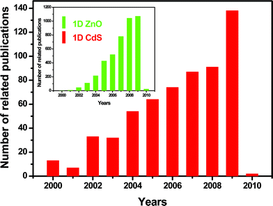 |
| | Fig. 1 Comparative publication statistics with respect to 1D nanostructures of CdS and ZnO. The data was complied on Jan. 22, 2010 using the database of the Institute of Scientific Information (ISI) and applying the following keywords that appear in the publication title: CdS (or cadmium sulfide) vs.ZnO (zinc oxide) combined with the nanowire, nanorod, nanotube, nanobelt, nanoribbon, nanosheet, nanotip, nanoring, nanofiber, nanohelix, nanoflower, nanobrush, or nanocomb terms. | |
This article provides a comprehensive review of the state-of-the-art research activities that focus on the rational synthesis, novel properties and unique applications of 1D CdSnanostructures. The review is divided into three main sections. The first section introduces the design and synthesis of 1D CdSnanostructures, such as nanowires, nanotubes, nanobelts, core/shell nanostructures, and other complex nanostructures. Next, several unique properties and applications based on 1D CdSnanostructures are presented, which include photoluminescence, cathodoluminescence, electrochemiluminescence, lasers, waveguides, modulators, solar cells, field-effect transistors, photodetectors, photocatalysts, field-emitters and nanogenerators. Finally, the review is concluded with certain perspectives and the author outlook on the future developments in this field.
2. Crystallographic structures of CdS
CdS have two kinds of structures, namely, the zinc blende crystal structure and the wurtzite structure. The zinc blende and wurtzite structures are cubic and hexagonal, respectively, and these two structures are rather close in some respects.15 As shown in Fig. 2, the stacking sequence of the close-packed planes of zinc blende (the (111) planes) is represented by the ABCABCABC repeating pattern, while that of wurtzite is represented by the ABABAB repeating pattern. Wurtzite CdS can be described as a number of alternating planes composed of tetrahedral-coordinated S2− and Cd2+ ions stacked along the c-axis.
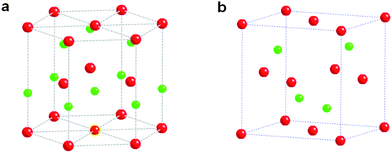 |
| | Fig. 2 The two kinds of structures of CdS: (a) hexagonal (wurtzite) and (b) cubic (zinc blende). Red and green balls represent Cd and S atoms, respectively. | |
Another important characteristic of CdS is its polar surfaces. The most common polar surface is the basal plane. The oppositely charged ions produce positively charged Cd-(0001) and S-(000![[1 with combining macron]](https://www.rsc.org/images/entities/char_0031_0304.gif) ) polar surfaces, resulting in a normal dipole moment and spontaneous polarization along the c-axis, as well as in divergence in surface energy. Wurtzite CdS possesses anisotropic growth for two reasons. One is that different crystallographic planes have different surface energies, and the other one is that their surface polarity and chemical activities differ.16
) polar surfaces, resulting in a normal dipole moment and spontaneous polarization along the c-axis, as well as in divergence in surface energy. Wurtzite CdS possesses anisotropic growth for two reasons. One is that different crystallographic planes have different surface energies, and the other one is that their surface polarity and chemical activities differ.16
3. Synthesis and construction of 1D CdSnanostructures
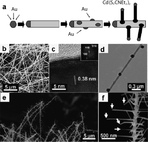
Vapor-phase synthesis is probably the most extensively explored approach to the formation of CdSnanowires (NWs). There are several processing parameters such as temperature, pressure, carrier gas, substrate and evaporation time that can be controlled and need to be properly selected before or during the vapor-phase synthesis. Several techniques have been utilized for the growth of CdSNWs, as shown in Table 1. For example, Lieber and co-workers demonstrated the first use of single-source molecular precursors for the growth of CdSNWs at a low temperature.17 By using well-defined molecular reactants, the authors were able to prepare single-crystalline CdSNWs with controlled diameters at high yield. Their synthetic approach follows the nanocluster-catalyzed vapor–liquid–solid (VLS) growth process, where Cd(S2CNEt2)2 molecular precursors serve as a source for Cd and S reactants (Fig. 3a). In this synthetic method, the single-source precursor undergoes thermal decomposition in the growth region and forms Cd–S–Au liquid solutions with the Au nanocluster catalysts. When the nanodroplets become saturated with the reactant, the nanowires start to grow. A representative SEM image of CdSNWs grown using 20 nm diameter catalyst clusters shows that this synthetic route produces nanowires in high yield and with uniform ca. 20 nm diameters (Fig. 3b). The HRTEM image and the corresponding Fourier transform (Fig. 3c) indicate that these CdSNWs are single-crystals growing along the [100] direction.17
Table 1 Summary of 1D CdSnanostructures synthesized using different methods
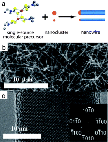 |
| | Fig. 3 (a) Nanowire growth from a single-source molecular precursor via a gold nanocluster-catalyzed vapor–liquid–solid mechanism; (b) SEM image of CdSnanowires synthesized using 20 nm gold nanoclusters; (c) HRTEM image of a 23 nm diameter nanowire grown from 20 nm gold nanoclusters, and two-dimensional Fourier transform of the TEM image. Reproduced from ref. 17 with permission. Copyright © 2003, American Chemical Society. | |
Ye and co-workers fabricated CdSNWs by the evaporation of self-made CdS powders without using any catalysts, and first observed the nucleation and growth process of CdSNWs during the typical vapor–solid synthesis.18 Their results indicated that three steps were involved in the growth of CdSNWs. Initially, CdS appeared as amorphous spherical particles (Fig. 4a), followed by nucleation of CdSnanorods (NRs) from cusps on the particle surface (Fig. 4b). Subsequently, NRs developed to NWs with matrix particles being consumed (Fig. 4c and d). Such a strategy could be optimized to grow CdSNWs of varying diameters and lengths for a variety of applications. Recently, we have also successfully synthesized CdSNWs by thermal evaporation of CdS powders in the presence of Au nanoparticles as catalysts at 850 °C. The diameter of the CdSNWs can be effectively controlled by varying the substrate temperature, which depends on the distance between the sources and substrate.9
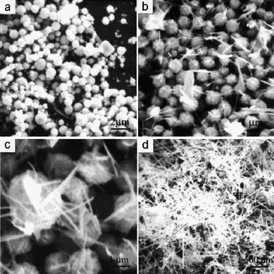 |
| | Fig. 4
SEM images of CdSnanostructures fabricated with different heating times: (a) 15 min, growth of CdS spheroids; (b) 30 min, nucleation of CdS short nanorods; (c, d) 45 min and 90 min, growth of CdSnanowires. Reproduced from ref. 18 with permission. Copyright © 2002, American Chemical Society. | |
3.3
CdS nanobelts
Unlike NWs and NTs, nanobelts (NBs) have a rectangular cross-section with well-defined geometry and high crystallinity. CdS NBs were first reported by Jiao and co-workers in 2003.23 Their method was based on the physical evaporation of a CdS powder under controlled conditions using a W foil covered with the 20 nm Au thin film as a substrate. The CdS NBs were formed in the 600–750 °C temperature zone. The lengths of the NBs range from 20 to 200 μm, and the widths range from 100 nm to 1.5 μm (Fig. 6a). At the ends of these CdS NBs, the width gradually decreases along the growth direction and terminates at a particle located at the belt tip. Both HRTEM and SAED characterizations (Fig. 6b) indicate that the CdS NBs are wurtzite single-crystals growing along the [100] direction.23 Subsequently, mass production of single-crystalline CdS NBs with controllable morphology and size was achieved by a simple thermal evaporation of CdS powders at 840 °C in the presence of Au catalysts.24 The CdS NBs have a typical width of about several hundred nanometres, a length of about ten to several hundred micrometres, a thickness of 30–60 nm (Fig. 6c) and a growth direction of <101> (Fig. 6d). The authors suggested that the growth of CdS NBs was initiated by the Au catalyst nanoparticlesvia a catalyst-assisted VLS process, and that side growth along the belt width direction took place via a vapor–solid (VS) process.24
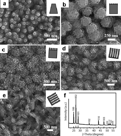
Growth of aligned nanostructures is important for applications in lasers, light-emitting diodes and field-effect transistors.25 Aligned growth of nanostructures can be achieved with the use of substrates and catalysts or seeds. Recently, we have successfully fabricated morphology-tunable ordered CdSnanostructure arrays by a two-step metal–organic chemical vapor deposition (MOCVD) process using Au nanocrystals as catalysts.11 As shown in Fig. 7, these ordered arrays uniformly and compactly cover the entire substrates, and the morphologies and alignments of nanostructure arrays are quite different for different distances between the precursors and a substrate. With increasing distance, the morphologies of CdSnanostructures vary from well-aligned truncated nanocone arrays (Fig. 7a), well-aligned nanorod arrays (Fig. 7b), well-aligned cleft nanorod arrays (Fig. 7c), quasi-aligned nanowire arrays (Fig. 7d), to nanowire arrays (Fig. 7e). The temperatures of the different zones are almost the same. An XRD pattern of the CdSnanostructures is shown in Fig. 7f. All the diffraction peaks can be readily indexed to a hexagonal wurtzite-structured CdS with the lattice parameters of a = 4.14 Å, c = 6.72 Å. The detailed microstructures of ordered CdSnanostructures were further studied by TEM. As can be derived from the SAED and HRTEM images, all the nanostructures are single crystals grown along the [001] direction. These CdSnanostructure arrays with similar structures and analogous synthetic conditions provide an ideal system for understanding the correlation between the structures and properties. We have thoroughly investigated the stimulated emission and field-emission of five ordered CdSnanostructure arrays, and found that they displayed notable differences in these properties, as discussed below.11
3.5.1 Core/shell nanostructures.
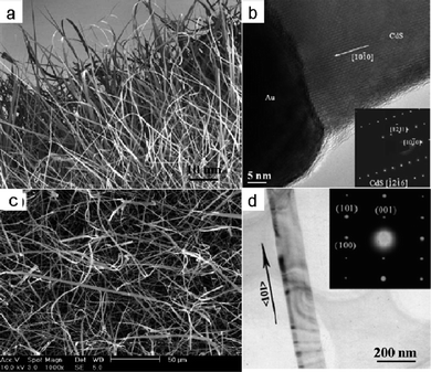
Core/shell nanostructures, e.g. coaxial nanostructures, are fundamentally interesting and have a high technological potential. In general, multi-step depositions involving sequential charges of desired source materials or surface modification by ambient species have been used to achieve a given architecture. For example, Sun and co-workers obtained TiO2/CdS core/shell NWs by coating TiO2NWs with CdSvia a chemical reduction process at room temperature (RT).76TiO2NWs were preliminarily fabricated by a hydrothermal method. The TiO2NWs present a smooth surface and uniform distribution, and have an average diameter of about 80 nm, as shown in Fig. 8a. The morphologies of the TiO2NWs changed remarkably when they were coated with CdS polycrystals. Fig. 8b shows a TEM image of the TiO2/CdS composite NWs. It demonstrates a sharp contrast between the outer and inner layer in the axis direction, confirming the core/shell heterostructure structure. The thickness of the CdS sheath could be controlled by changing the concentration of the S precursor and the corresponding stoichiometric amount of anhydrous CdCl2. A schematic diagram of the multi-step mechanism is depicted in Fig. 8c and detailed results can be found in ref. 76. Unlike the multi-step strategy, Lu and co-workers fabricated CdS/ZnS core/shell NWsvia a one-step MOCVD process with a co-fed single source of CdS and ZnS.77 The co-fed precursors of CdS(Cd(S2CN(C3H7)2)2, denoted as Cd33 and ZnS ([Zn(S2CN(Bu2)2]2, denoted as Zn44 were designed to guarantee a sufficient reactivity difference and to enable sequential reaction for in situ formation of the core/shell structures. The authors suggested that Cd33 was thermally decomposed first to form the core CdSNWsvia a VLS mechanism in the presence of Au catalyst, and these NWs then served as the catalyst to promote the thermal decomposition of Zn44. The later-formed ZnS was expected to grow on the surface of the first-formed CdSNWs, and thus coaxial CdS/ZnSNWs were fabricated. A TEM image of CdS/ZnS core/shell NWs (Fig. 8d) shows that the thickness of the shell layer is about 10 nm, while the diameter of the core is around 30 nm. The coaxial NWs exhibit some microtwins and stacking faults at the core/shell interface and in the shell region (indicated by arrows in Fig. 8e). The closeness of the (111) planes of cubic ZnS and the (101) planes of hexagonal CdS enabled the growth of coaxial ZnS shells on the CdS core wires via a minor atomic-level surface reconstruction. Furthermore, other CdS-based core/shell nanostructures, such as CdS/Si, CdS/CdSe, CdS/C, InP/CdSnanostructures, have been constructed, as shown in Table 2.
Table 2 Representative 1D CdS-based nanostructures of complex shapes and microstructures and their synthesis methods
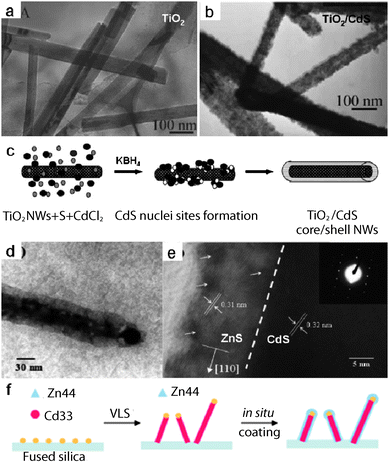 |
| | Fig. 8 (a, b) TEM images of TiO2nanowires and TiO2/CdS core/shell nanowires; (c) Schematic illustration of the multi-step growth mechanism. Reproduced from ref. 76 with permission. Copyright © 2004, Royal Society of Chemistry. (d) TEM image, (e) HRTEM image and (f) possible growth mechanism of CdS/ZnS core/shell nanowires fabricated by a one-step MOCVD process with co-fed single source precursors of CdS and ZnS. Reproduced from ref. 77 with permission. Copyright © 2004, Royal Society of Chemistry. | |
3.5.2
CdS rocket-like tetrapodal nanorods.
Using the idea of epitaxial growth, we fabricated rocket-like CdS tetrapods (RTPs) via a one-step seed-epitaxial MOCVD approach by thermal decomposition of Cd(S2CNEt2)2 powders using Ag particles and cubic CdSenanocrystals (NCs) as catalysts.78–81 This bottom-up method uses Ag particles to initiate and guide the preferential orientation of the axial nanorods, while the epitaxial growth of wurtzite-structured branches occurs on the cubic CdSe seeds. The SEM image shows that the as-synthesized CdSnanostructures, which appear gray, evenly cover the Si deposition substrate. Each nanorod of CdS RTPs consists of three branches of 500 nm in length, and the stem of 200 nm in diameter. The nanorods keep their threefold symmetry of parallel branches around the central stems. Unlike traditional tetrapod structures, the central stem was longer than the branches and passed through the tetrapod center. These structural characters are easily noticed while looking at the SEM and TEM images (Fig. 9a–d). The HRTEM image and SAED pattern indicate that the stem and the branches of the CdS RTP structure are single crystals and grow along the [001] direction. In order to understand the formation mechanism of the CdS RTPs, we have conducted additional experiments. These indicated that the Ag particles and cubic CdSeNCs play an important role in the structure formation. (1) Only using Ag particles, highly dense CdS nanoneedles were found to cover the entire substrate. The morphology and intrinsic structure were similar to the axial rods of the CdS RTPs. (2) Only using cubic CdSeNCs, some branched CdSnanostructures could be obtained, which were similar to the branches of the RTPs. (3) When the amount of Ag particles decreased, the quantity of CdS RTPs was reduced accordingly. (4) Using wurtzite NCs, CdS nanoneedles were obtained which showed a similar morphology to those formed in the absence of seeds. (5) Using mixed NCs, CdS nanoneedles and RTPs were found to exist, also no arms were observed on some CdSnanorods. These results confirm that Ag particles and the zinc blende CdSe seeds are crucial to the preparation of CdS RTPs using the seed-epitaxial method. On the basis of the above analysis, the formation process of the CdS RTPs is proposed, a schematic description of which is given in Fig. 9e and a detailed growth mechanism is discussed in ref. 78.
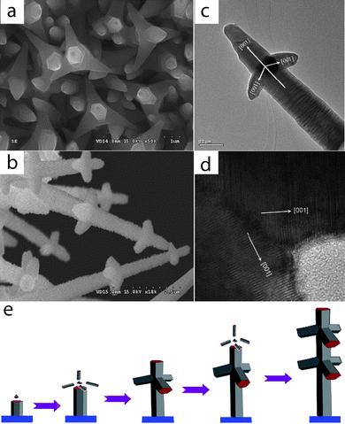 |
| | Fig. 9 (a) SEM image of CdS rocket-like tetrapods (RTPs); (b) SEM image of two-level RTPs; (c) TEM image of a CdS RTP; and (d) HRTEM image of the interface between the branch and the central nanorod of the CdS RTP; (e) Schematic diagram for the growth mechanism of the CdS RTPs. Reproduced from ref. 78. Copyright © 2007, American Chemical Society. | |
3.5.3 ZnxCd1−xS nanocombs and zigzag nanowires.
Recent advances in ternary semiconductor nanostructures have shown that their bandgaps and thus their physical properties can be tuned by changing constituent stoichiometries. Lee and co-workers fabricated ZnxCd1−xS nanoribbons of variable compositions (0 ≤ x ≤ 1) by combining laser ablation of CdS and thermal evaporation of ZnS at 950 °C.82 The ZnxCd1−xS nanoribbons had thicknesses of 50–80 nm, widths of 0.5–5.0 μm, and lengths up to several hundreds of micrometres. Recently, we developed a low-temperature route for the preparation of single-crystalline ternary ZnxCd1−xS nanocombs and zigzag NWsvia a one-step MOCVD route by heating a mixture of Zn(S2CNEt2)2 and Cd(S2CNEt2)2 powders to 400–420 °C.83–85Fig. 10a shows the typical growth of a comb-like structure, with one side flat and the other side with short nanoteeth. The diameters of the comb ribbons range from 500 to 800 nm, and their lengths are in the range of 2–50 μm. These teeth have a length of 300–800 nm and a width of 30–100 nm. Fig. 10b shows a SEM image of typical zigzag NWs. These NWs have diameters of 200–300 nm, widths of 200–300 nm and lengths of up to tens of micrometres. TEM results indicate that these NWs are single-crystalline, with the [001] axis after changing the growth direction from [13a2/2c2] to [13a2/2c2] (a, c are the respective lattice constants of the a-axis and c-axis). The compositions x of the ZnxCd1−xS nanocombs and NWs are 0.54 and 0.78, respectively. A study on the growth mechanism showed that the shear strain, as well as slight fluctuation of the reaction conditions, can change the growth direction of the nanowires and the asymmetric growth behavior of the nanocombs is induced by surface polarization.83,84
 |
| | Fig. 10 (a) SEM image of ZnxCd1−xS nanocombs. Reproduced from ref. 83 with permission. Copyright © 2006, Elsevier. (b) SEM image of ZnxCd1−xS zigzag nanowires. Reproduced from ref. 84 with permission. Copyright © 2006, Institute of Physics. | |
3.5.4
ZnS-CdS branched nanowire heterostructures.
Agarwal and co-workers reported the fabrication of branched nanowire heterostructures whose backbones and branches made of ZnS and CdS had respectively been assembled.86 Growth of branches and backbones with a control over the compositions was performed via sequential seeding of gold nanocluster catalysts. The growth method of ZnS (CdS) NWs was based on a MOCVD process using single molecular precursors, where Zn(S2CNEt2)2 and Cd(S2CNEt2)2) were used to grow ZnS and CdSNWs. The strategy to synthesize branched nanowire heterostructures is illustrated in Fig. 11a. First, ZnSNW backbones with controlled compositions and diameters were fabricated via VLS synthesis by using Zn(S2CNEt2)2 as the precursor and monodispersed Au nanoclusters as the catalyst. The diameters of NWs ranged approximately from 80 to 120 nm, and the NW lengths were typically greater than 10 μm, as shown in Fig. 11b. The TEM results indicated that the majority of the ZnSNWs had been grown along the [100] direction (Fig. 11c). Second, these ZnSNW backbones were seeded with Au colloidal solution followed by air-drying for secondary catalystdeposition. Fig. 11d shows a TEM image of an isolated ZnSNW after the Au catalyst deposition revealing the Au nanoparticles attached to ZnSNWs. Finally, the branches were grown by placing the ZnSNWs with secondary catalysts deposited on them in a furnace under a flow of CdS precursor materials. The branched NWs were found to be densely placed on the substrate as shown in Fig. 11e. At a higher magnification (Fig. 11f), the Au nanoparticles are clearly seen at the tips of branches (marked by arrows in Fig. 11f). The diameter distribution of the branches is similar to the size distribution of the Au catalysts. Electron microscopy studies indicate that the growth of heterostructures branches occurs epitaxially while maintaining a single-crystalline structure. These new NW heterostructures, distinct from NW axial and radial heterostructures, will be useful as nanoelectronic and photonic building blocks to control the generation and transport of carriers and photons in three dimensions.86
 |
| | Fig. 11 (a) Schematics illustrating the synthesis of nanowire branched heterostructures; (b, c) SEM and HRTEM images of ZnS nanowire backbones; (d) TEM image of Au catalysts deposited on ZnSnanowires; (e) SEM image of branched structures showing multiple branches spread out from each backbone nanowire; (f) SEM image of an isolated branched structure showing Au catalysts at the tips of branches, marked by arrows. Reproduced from ref. 86 with permission. Copyright © 2007, American Chemical Society. | |
4. Properties, potential applications, and novel devices of 1D CdSnanostructures
4.1 Optical Properties
4.1.1 Photoluminescence.
As the literature documents, for a large number of 1D CdSnanostructures of various shapes synthesized using different methods, in general, two emission bands are observed due to excitonic and trapped state luminescence.108 Shen and co-workers reported the fabrication of single-crystalline CdS microbelts by a modified thermal evaporation method, in which an adiabatic layer was used to provide an abrupt temperature decrease and high gas concentration for the microbelt growth.66 These microbelts have typical lengths of tens to several hundreds of micrometres, widths up to 10 μm, and thickness of about 70 nm, as shown in Fig. 12a. After examining the RT photoluminescence (PL), as depicted in Fig. 12b, two emission bands have been detected, namely, a sharp and strong emission band located at 2.38 eV (521 nm) and a weak and broad emission centered at 2.07 eV (599 nm). These authors suggested that the strong emission originated from the recombination of free excitons. The weak emission was attributed to deep levels associated with S vacancies, extrinsic defects and impurities.66 Zhao and co-workers fabricated multi-armed CdSnanorodsvia a simple surfactant-ligand co-assisted solvothermal process. The length of CdSnanorods was controlled from 100 nm up to a micrometre by changing the relative concentration of dodecylthiol and EDA. A strong emission peak centered at 710 nm was observed in the PL spectrum, and the authors attributed it to a self-activated emission of CdS.109 Zou and co-workers reported a strong near-band-edge (NBE) emission and a weak red emission at ca. 502–520 nm and 716 nm from high-quality 6-fold symmetry-branched CdSnanostructures, respectively. The authors proved that the red emission arose from transitions of electrons trapped at the surface states to the valence band of CdS crystals.105
4.1.2 Cathodoluminescence.
Cathodoluminescence (CL) is an optoelectrical phenomenon wherein a beam of electrons is generated by an electron gun and interacts with a luminescent material, such as phosphor, causing the material to emit light. It is a useful technique for characterization of nanostructure optical properties because of its high spatial resolution and structural information obtained by using secondary electron (SE) imaging.110,111 Recently, we fabricated high-quality, uniform 1D CdS micro/nanostructures with different morphologies—microrods, nanotips and sub-microwires—through an easy and effective thermal evaporation process, and systematically investigated their cathodoluminescence and field-emission properties.9 The representative morphologies and structures of the produced CdS micro/nanostructures were analyzed by SEM. Fig. 13a is the SEM image of a product obtained at 800 °C using 20 nm Au nanoparticles as a catalyst. The microrods have diameters of ca. 500–1200 nm and lengths up to several micrometres, and exhibit hexagon-like cross-sections. With a decrease in the substrate temperature and without using a catalyst, the morphology changes from microrods to nanotips. The SEM image in Fig. 13b shows that the CdS nanotips are composed of branched nanostructures with needle-shaped ends. When the source temperature becomes higher (850 °C), and under use of sputtered 10 nm Au nanocrystals as a catalyst, sub-microwires are formed. The SEM images (Fig. 13c) show that the sub-microwires have a relatively uniform diameter of 450 nm and a circular cross-section. The diameters can effectively be controlled by varying the substrate temperature (the latter depends on the distance between the sources and substrates). Fig. 13d depicts a SEM image of sub-microwires with a diameter of ∼200 nm fabricated at a lower substrate temperature (compared to sample c) while keeping the other experimental conditions unchanged. The wire diameters decrease, while the lengths do not change. All the CdSnanostructures are single crystals with a hexagonal wurtzite structure grown along the [001] direction. For CdS nanotips, various defects are seen along the nanotip, and the defect concentration decreases towards the tip-end. The detailed growth conditions and structure characteristics are presented in ref. 9.
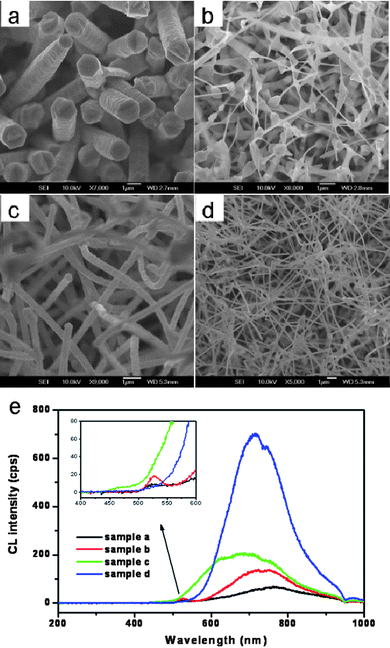 |
| | Fig. 13 Typical SEM images of several CdS micro/nanostructures fabricated by an easy and effective thermal evaporation process: (a) microrods; (b) nanotips; (c) thick sub-microwires; (d) thin sub-microwires; (e) corresponding CL spectra. Reproduced from ref. 9 with permission. Copyright © 2009, Wiley-VCH. | |
Fig. 13e illustrates four typical CL spectra taken from four representative nanostructures: microrods, nanotips, thick and thin sub-microwires. In the CL spectra of the microrods and nanotips, two typical emission peaks (a weak luminescence emission peak at 525 nm (527 nm for nanotips) and a broad emission at 764 nm (735 nm for nanotips)) are observed, which are assigned to the NBE and defect-level (DL) emissions, respectively. In the case of thick and thin sub-microwires, only DL emission is present and no NBE emission is detected. The absence of NBE emission from these sub-microwires demonstrates that they are prone to many intrinsic defects, such as vacancies and interstitials, which form new energy levels thus hindering the NBE emission. In order to study spatial variation of optical properties and gain an insight into the origin of the DL emission, we have recorded CL spectra at spots with different diameters on a series of individual nanotips (Fig. 14a–c). A significant decrease in the DL/NBE intensity ratio is observed along a tapered nanotip towards a smaller diameter part (Fig. 14e). We presumed that the origin of DL was related to the peculiar defect distribution in the nanotip bodies, as verified by HRTEM. The defect concentrations decreased with diameter shrinking, thus the DL emissions also diminished.9
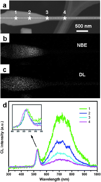 |
| | Fig. 14 (a) SEM image of a nanotip with four spots marked by white “stars”. (b, c) The corresponding CL images recorded at 530 nm and 725 nm; (d) CL spectra from the four spots using intensity normalized to the NBE emission peak, respectively. The inset highlights the spectra in the range of 480 to 580 nm. Reproduced from ref. 9 with permission. Copyright © 2009, Wiley-VCH. | |
4.1.3 Optically-driven lasers.
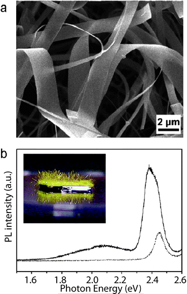
Nanowires with flat ends can be exploited as optical resonance cavities to generate coherent light at the nanoscale. Yang and co-workers first observed room-temperature UV-lasing from arrays of ZnO nanorods grown on sapphire substrates using the VLS method.112 As shown before, we fabricated highly ordered CdSnanostructure arrays, and their uniform dimensions and good crystallinities indicated that stimulated emission or lasing under high excitation may be realized in them. Fig. 15a displays the power-dependent PL spectra of quasi-aligned CdSNW arrays excited by femtosecond laser pulses with various power densities at room temperature. At a low excitation intensity, a broad and weak band appears at 500.1 nm (2.480 eV), which was attributed to a spontaneous exciton transition at the CdS bandgap. When the excitation power density increased to ∼5.1 × 10⁻⁴ J cm−2, a new sideband appeared at 515.6 nm (2.405 eV), at the lower energy side of the broad mainband. This sideband with a ∼75 meV red-shift was attributed to the E-2LO phonon band, since the 2LO phonon energy (ca. 76 meV) is close to the observed red-shift and larger than the available thermal energy at room temperature (∼26 meV). This peak had a full width at a half-maximum (FWHM) of 5 nm, which was lower than for spontaneous exciton emission, and its output intensity increased rapidly, indicating a lasing action. Fig. 15b plots the excitation power dependence of the emission intensity for spectral positions at 500 and 516 nm. It clearly shows that the PL intensity at 500 nm has an approximately linear increase with rising of the excitation power, whereas the emission intensity at 516 nm has a superlinear dependence on the excitation power, with a threshold at 4.5 × 10⁻⁴ J cm−2. The supralinear increase in emission intensity is a characteristic of the amplified stimulated emission and lasing. We also investigated the lasing threshold of other CdSnanostructures. It was found that well-aligned nanorod arrays had a lower threshold (0.8 × 10⁻⁴ J cm−2), compared to the well-aligned truncated nanocone arrays (1.2 × 10⁻⁴ J cm−2), well-aligned cleft-nanorod arrays (1.0 × 10⁻⁴ J cm−2) and quasi-aligned nanowire arrays (4.5 × 10⁻⁴ J cm−2). We didn't observe the stimulated emission phenomenon in the nanowire arrays (sample e). We suggested that the lasing threshold was mainly dependent on the orientation of an array. The samples a–c had similar orientations, which resulted in similar lower thresholds. Sample d had the poorest orientation, leading to a higher threshold. When the alignment deteriorated, no stimulated emission was observed. A detailed discussion is presented in ref. 11.
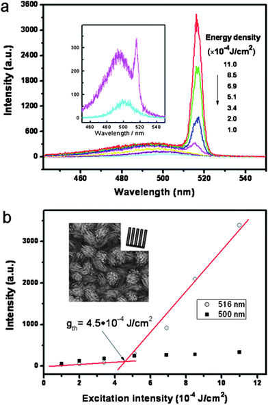 |
| | Fig. 15 (a) Power-dependent PL spectra of quasi-aligned CdSnanowire arrays excited by a femtosecond laser with various excitation power densities at room temperature; the inset is an enlargement of the two curves at 1.0 × 10⁻⁴ and 5.1 × 10⁻⁴ J cm−2; (b) Excitation power dependence of the emission intensity for spectra positions at 500 and 516 nm. Reproduced from ref. 11 with permission. Copyright © 2009, American Chemical Society. | |
4.1.4 Electrically driven lasers.
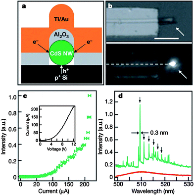
Electrically driven semiconductor lasers are used in technologies ranging from telecommunications and information storage to medical diagnostics and therapeutics. Lieber and co-workers first implemented nanoscale injection lasers based on a CdS single nanowire and described a powerful approach for production of an integrated electrically driven photonic device in 2003.12,113 The devices were fabricated by assembling CdSNWs on heavily doped p-Si on insulator substrates, followed by electron beam (EB) lithography and EB deposition of 60–80 nm Al2O3, 40 nm Ti and 200 nm Au. One end of the NW was left uncovered for emission output from the device, as shown in Fig. 16a and 16b. This structure produced the hybrid n-CdS/p-Si heterojunctions needed for an injection device. Images of the RT electroluminescence produced in forward bias from these hybrid structures (Fig. 16b) exhibited strong emission from the exposed CdSnanowire ends. Measurements of the NW and electroluminescence intensity versus current (Fig. 16c) showed an initial increase in the intensity at about 90 μA and then a much more rapid and highly nonlinear increase at about 200 μA. At low injection currents, the spectrum of the end emission (Fig. 16d) revealed a broad peak with FWHM ≈ 18 nm, consistent with spontaneous emission, but above the 200 μA threshold the spectrum quickly collapsed into a limited number of very sharp peaks with a dominant emission line at 509.6 nm. The sharp peaks emerged from only part of the spontaneous emission spectrum and had an average spacing of about 1.8 nm, which was consistent with the Febry–Perot cavity mode for the length of the nanowire device. These observations provided strong evidence for lasing from single-nanowire injection structures at RT.12
 |
| | Fig. 16 A nanowire electrical injection laser: (a) Schematic image showing the cross-section of the device structure. (b) Top panel shows an optical image of a device described in (a). Bottom panel shows an electroluminescence image recorded from this device at RT with in injection current of about 80 μA. (c) Emission intensity versus injection current. (d) Electroluminescence spectra obtained from the nanowire end with injection currents of 120 μA (red) and 210 μA (green). Reproduced from ref. 12 with permission. Copyright © 2003, Nature Publishing Group. | |
4.1.5 Waveguides.
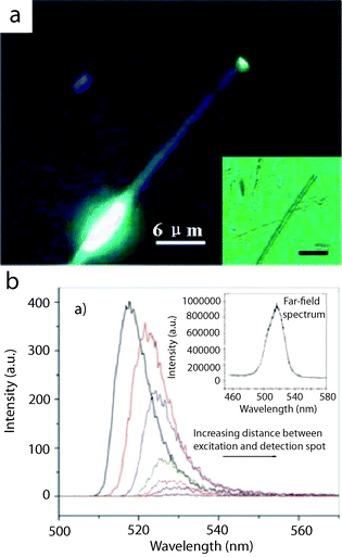
1D nanostructures with cavities are expected to function as waveguides for guiding and manipulating light on the sub-wavelength scale. Yang's and Lieber's groups performed pioneering and extraordinary work on ZnOnanowires, SnO2nanoribbons and CdSnanowires. These structures can successfully work as optical waveguides for integrating sub-wavelength photonic components.114,115 Zou and co-workers quantitatively and systematically investigated guided band-edge luminescence through individual CdSnanoribbons by imaging the spatially localized PL intensity and simultaneously recording the PL spectra at different traveling distances using near-field scanning optical microscopy (NSOM).41 Their results demonstrated that locally produced band-edge PL could be effectively transported several hundred micrometres away along a single CdSnanoribbon (Fig. 17a). The emission bands showed a significant red-shift with respect to increasing traveling distances, as illustrated in Fig. 17b.
4.1.6 Electro-optical modulator (EOM).
Electro-optical modulators (EOMs) are used to switch the output of semiconductor lasers. Lieber and co-workers first reported the integration of EOMs on nanowire laser cavities, and demonstrated the electric field modulation of lasing in CdSNW lasers.116 The CdSNWs were single-crystalline with diameters of ∼100 nm and lengths of more than 10 μm. EOM devices with a parallel-plate structure (Fig. 18a) were placed in a uniform electric field over a length L of the nanowire. Fig. 18b shows the modulation of the output signal of a representative CdSNW-EOM with L = 6 μm and a SiO2 dielectric layer thickness ttop = tbot = 50 nm, demonstrating that under variation of the applied voltage, V, from 0 to 30 V, the exciton lasing line (489 nm) is significantly attenuated, with no resolvable shift in the peak wavelength, while the spontaneous emission features (514 nm) show a much smaller attenuation. For a given wavelength and V, the modulation, M, is given by (ION/IOFF) − 1, where ION and IOFF are the intensities with and without V. Plots of M vs. V for both the exciton lasing line and the free electron-bound hole (FEBH) feature (Fig. 18c) exhibit a linear dependence on V over the ±50 V range tested. Notably, the 489 nm lasing line is modulated by 40% at 45 V, which is > 2 × the modulation of the FEBH feature.116
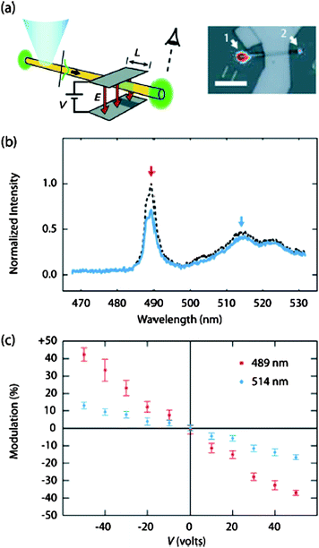 |
| | Fig. 18 (a) Diagram indicating the excitation site, region of field modulation, and observed NW end; (b) Emission spectrum of a CdSNW laser showing effect of a 30 V signal; (c) Modulation Mvs.V at the two indicated wavelengths from the EOM-laser in (b). Reproduced from ref. 116 with permission. Copyright © 2005, American Institute of Physics. | |
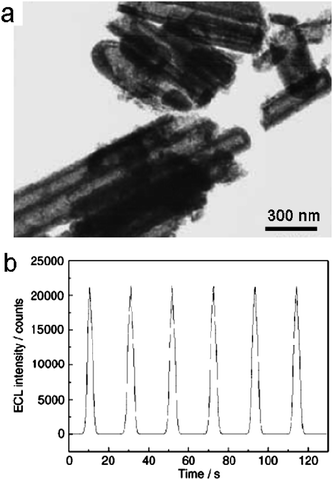
4.1.7 Electrochemiluminescence.
Electrochemiluminescence (ECL) involves the generation of species at electrode surfaces which then undergo electron-transfer reactions to form excited states that emit light.117,118 Zhu and co-workers reported the stable and highly enhanced ECL from CdSNTs fabricated by a double-template method.119 These NTs had an external diameter of 140 nm and an internal diameter of 100 nm. They were composed of small nanocrystalline particles with diameters of 7–8 nm, as shown in Fig. 19a. The ECL behavior of the CdSNTs at a carbon-paste electrode in aqueous solution was studied using conventional cyclic voltammetry (CV). Fig. 19b shows the ECL emission of CdSNTs under continuous potential scanning for six cycles. The electrode potential was cycled between 0.1 V and −1.2 V at a scan rate of 100 mV s−1. As the electrode potential became more negative, electrons were injected into the CdSnanocrystals and electrogenerated anion radials (CdS−˙) were formed. Concurrently, S2O82− ions were added as a co-reactant to produce a strong oxidant, SO4−˙. The formed sulfate radicals could react with the negatively changed CdSnanocrystals to produce excited states and then generate high-intensity light emission.
| S2O82− + e−→SO42− + SO4−˙ |
| CdS−˙ + SO42− → CdS* + SO42− |
In the ECL curve, the light emission displayed quite good stability and enhanced intensity, which could be attributed to the aggregation morphology of the CdSNTs and the addition of the co-reactant. The CdSNTs composed of compact nanocrystals exhibited strong ECL, which might find useful applications in biodetection.119
4.2 Solar cells
Solar energy represents one of the most abundant and yet least harvested sources of renewable energy. Of particular interest to cost-effective solar cells is to use novel device structures and materials processing for enabling acceptable efficiencies.120 Recently, Javey and co-workers demonstrated a novel photovoltaic structure (Fig. 20a) that incorporates 3D single-crystalline n-CdS nanopillars (Fig. 20b) embedded in polycrystalline thin films of p-CdTe. The device enables high absorption of light and efficient collection of the carriers.121 An optical image of fully fabricated n-CdS/p-CdTe solar nanopillar (SNOP) cells is presented in Fig. 20c with an active surface area of 5 × 8 mm. The performance was characterized by using a solar simulator (LS1000, Solar Light) without a heat sink. Fig. 20d demonstrates the I–V characteristics of a typical cell under different illumination intensities, P, ranging from 17 to 100 mW cm−2 (AM 1.5 G). An efficiency (η) of ∼6% was obtained with an open circuit voltage Voc ∼ 0.62 V, short circuit current density Jsc ∼ 21 mA cm−2 and fill factor FF ∼ 0.43 under AM 1.5 G illumination (Fig. 20e, f). These results were better than for most of the reported photovoltaics based on nanostructured materials.122,123 Based on their simulation, the authors speculated that the efficiency could be readily enhanced in the future through further device and materials optimization, for instance, by using top contacts with higher optical transparency and lower parasitic resistances.121
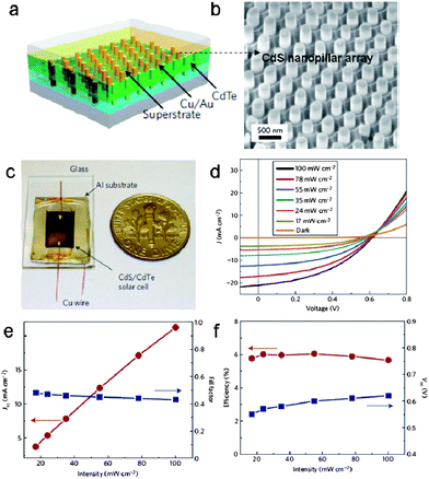 |
| | Fig. 20 (a) Schematic diagram of CdS/CdTe solar nanopillar (SNOP) cells; (b) SEM image of CdS nanopillar arrays; (c) An optical image of fully fabricated SNOP cell bonded to a glass substrate; (d) I–V characteristics at different illumination intensities; (e) The short-circuit current density, Jsc shows a near-linear dependence on the illumination intensity, whereas the fill factor, FF, slightly decreases with an increase of the intensity; (f) The open-circuit voltage, Voc, slightly increases with the intensity and the solar energy conversion efficiency is nearly independent of the illumination intensity for P = 17–100 mW cm−2. Reproduced from ref. 121 with permission. Copyright © 2009, Nature Publishing Group. | |
4.3 Field-effect transistors (FETs)
4.3.1 Metal–insulator–semiconductor field-effect transistors (MISFETs).
1D nanostructures have been incorporated into field-effect transistors (FET) to serve as the fundamental building blocks of electronic devices such as logic gates, computing circuits and sensors. In brief, the fabrication process can be described as follows. Nanowires are first dispersed in a solvent, and then deposited on a SiO2/Si substrate. The bottom substrate underneath the SiO2 layer is then degenerately doped (p++ or n++), serving as the backgate. Two metal contacts, corresponding to the source and drain electrodes, are defined by either photolithography or electron beam lithography followed by evaporation of suitable metal contacts. This FET is a metal–insulator–semiconductor field-effect transistor (MISFET), shown in Fig. 21a. Dai and co-workers fabricated high-quality n-type CdS NBs via an in situ In doping CVD method and incorporated them into MISFETs (Fig. 21b). The electron concentrations and motilities of these CdS NBs were around 1.0 × 10¹⁶–3.0 × 1017 cm−3 and 100–350 cm2 V−1 s, respectively. The on-off ratio was greater than 108 and the sub-threshold swing was smaller than 65 mV/decade at RT.124
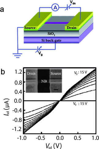 |
| | Fig. 21 (a) Schematics of a single NW FET; (b) SEM image of a single CdS NB MISFET and Isd–Vsd curves with Vg from −15 V to 15 V. Reproduced from ref. 124 with permission. Copyright © 2006, American Institute of Physics. | |
4.3.2 Metal–semiconductor field-effect transistors (MESFETs).
A metal–semiconductor field-effect transistor (MESFET) is another important type of FET. Different from a MISFET, the source–drain current is controlled by a Schottky gate in a MESFET. The performance of the MESFET is determined by the quality of Schottky and ohmic contacts to the semiconductor. Dai and co-workers fabricated MESFETs based on single CdS NBs (Fig. 22a).125–127 The single CdS NB MESFETs exhibited n-channel (normally on depletion mode), low threshold voltage (∼1.56 V), high transconductance (∼3.5 μS), low sub-threshold swing (∼45 mV/decade), and high current ratio (∼2 × 10⁸) (Fig. 22b).
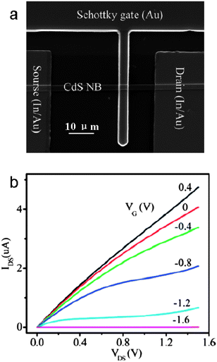 |
| | Fig. 22 (a) SEM image of a single CdS NB MESFET; (b) Ids–Vds curves measured at various gate voltages. Reproduced from ref. 125 with permission. Copyright © 2007, American Chemical Society. | |
4.3.3 Logic circuits.
Field-effect transistors with electrically controlled “on” and “off” switching functions are the fundamental elements to construct higher level circuits, for instance, logic gates, which are the key components in an integrated computation circuit.128 Dai and co-workers have designed and constructed a high-performance NOT logic gate (inverter), NOR, and NAND gate on CdSNWs.62,69,129 The basic components of these devices are high-performance MESFETs made on single CdSNWs where top Schottky gates have been employed, as shown in Fig. 23.
 |
| | Fig. 23 (a) SEM image of an inverter (NOT logic gate) made on one single CdSNW; (b) Transfer characteristic of the inverter depicted in (a); (c, d) Output voltage of a CdSNW “NOR” and “NAND” gate for the four possible input states, respectively. Reproduced from ref. 129 with permission. Copyright © 2007, American Chemical Society. | |
4.4 Photodetectors
Among all the nanoscale devices, the photodetectors are critical for applications as binary switches in imaging techniques and light-wave communications, as well as in future memory storage and optoelectronic circuits.130–137 With large surface-to-volume ratios and Debye length comparable to their small size, 1D CdSnanostructures have been widely used for visible-light sensors or photodetectors with high sensitivity and selectivity.74,138–142 For example, individual CdSnanoribbon-based visible-light photodetectors with high photosensitivity and high photoresponse speed were reported by Lee et al. in 2006.74 The CdSnanoribbons used in the experiments were grown by a CVD method. The width and thickness of the nanoribbons were in the range of 2–40 μm and 10–60 nm, respectively. Ti/Au parallel electrodes were deposited on the nanoribbon dispersed on a SiO2/Si substrate, and the uncovered part of the ribbon was exposed to the incident light, as shown in the inset of Fig. 24a. Fig. 24a shows the current–voltage (I–V) characteristics of an CdSnanoribbon (width ∼10.4 μm and thickness ∼30 nm) illuminated with light of different wavelengths (λ). The approximately linear shape of the curves reveals good ohmic contacts of the nanoribbon with the electrodes. It is noted that the photoconductance (Gpho) at zero bias is highly wavelength sensitive: Gpho = 0.793 nS for λ = 500 nm, and 128 nS for λ = 490 nm, vs.Gpho = 0.021 nS measured in the dark. Fig. 24b shows the time response of the CdSnanoribbon device to the pulsed incident light (490 nm). It indicates that the response of the CdSnanoribbon to the incident light is very fast. It shows excellent stability and repeatability as well. Close examination reveals a rise time and fall time of 747 μS and 794 μS, respectively. Furthermore, the absorption of ambient gas (mainly oxygen) can significantly change the photosensitivity of CdSnanoribbons. These demonstrations suggest that the CdSnanoribbons can be a perfect candidate for applications in high-sensitivity and high-speed nanoscale photodetectors and photoelectronic switches.74
 |
| | Fig. 24 (a) I–V curves of a CdS single nanoribbon illuminated with light of different wavelengths; (b) Time response of the CdSnanoribbon to the pulsed incidence light (490 nm, 1.8 mW cm−2). Reproduced from ref. 74 with permission. Copyright © 2006, American Chemical Society. | |
4.5 Photocatalysis
As is known, CdS has been used as a semiconductor-type photocatalyst for the photoreductive dehalogenation of halogenated benzene derivatives, photocatalytic degradation of water pollutants, and photocatalytic reduction of toxic metal ions.143,144 Yu and co-workers investigated the photocatalytic activity of branched CdSnanowires by choosing photocatalytic degradation of acid fuchsine as a test reaction.145 The characteristic absorption of acid fuchsine at about 543 nm was chosen as the monitored parameter for the photocatalytic degradation process. Fig. 25 is the time-dependent UV–vis absorption spectra of photocatalyst-degraded acid fuchsine, which shows that the absorbance intensity for the peak at 543 nm decreases very quickly once the branched CdSnanowires are added, corresponding to the immediate color change. The results suggested that the branched CdSnanowires might have a high BET surface and thus could absorb the dye molecules more efficiently. Under increasing exposure time, the typical sharp peak at 543 nm diminished gradually and completely vanished after 45 min. The authors also compared the catalyst activity of the branched CdSnanowires with Degussa P25 TiO2, and found that the branched CdSnanowires photocatalyst showed much higher activity that that of Degussa P25.145 Recently, Sun and co-workers have fabricated pure and Cd-rich CdSnanotubes with one sealed end and one open end and investigated their photocatalytic properties.57 Both the Cd-rich and the pure CdSnanotubes possessed a high photocatalytic activity, as measured by the decomposition of methylene blue (MB). Under UV light, Cd-rich CdSnanotubes exhibited a degradation efficiency of up to 98% in only 24 min, and the same weight of pure CdSnanotubes reached up to 95%. Under visible light, the degradation efficiency reduced to 60% and 46%, respectively. The Cd-rich CdSnanotubes possessed a higher photocatalytic activity than the pure CdSnanotubes in UV, and especially in the visible region.57
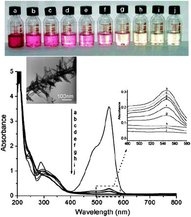 |
| | Fig. 25 Time-dependent color change and corresponding time-dependent absorption spectra of a solution of acid fuchsine (5 × 10⁻⁵ M, 20 mL) in the presence of branched CdSnanowires after its exposure to UV light: (a) initial solution; (b) after adding the CdSnanowires; and (c–j) after exposure to UV light for 5, 15, 30, 45, 75, 125, 175, and 235 min, respectively. The inset shows the enlarged temporal evolution of absorption (b–j). Reproduced from ref. 145 with permission. Copyright © 2006, American Chemical Society. | |
4.6 Field-emission properties
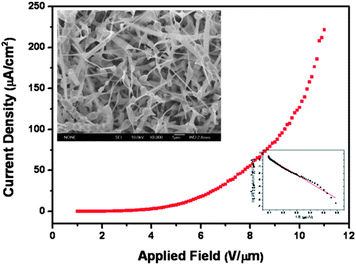
Field-emission (FE), also known as Fowler–Nordheim (FN) tunneling, is a form of quantum tunneling in which electrons pass from an emitting material to the anode through a barrier in the presence of a high electric field. It is one of the main features of nanomaterials and nanostructures, and is of great commercial interest in displays and other electronic devices.146–149 As is known, the electron emitters made of materials with a low work function and a high field-enhancement factor should greatly enhance the FE current at a low applied turn-on voltage.150 The work function for CdS (4.2 eV) is lower than that in many popular FE materials, such as C nanotubes (5.0 eV), ZnO (5.3 eV), ZnS (7.0 eV). Thus CdS is one of the best FE candidates. Our recent results show that CdS nanotips with sharp tips possess a low turn-on field of 5.28 V μm−1 and a high field-enhancement factor of 4819, Fig. 26. The data suggests that the CdS nanotips may rival or even surpass those of ZnO, ZnS, Si, SiC and AlN nanowires/nanobelts and C nanotubes for emitter applications.9 Furthermore, we also systematically investigated the correlation between morphologies, alignments and field-emission performance of five ordered CdSnanostructure arrays, and found that both of the alignments and aspect ratios greatly affected the field-emission properties: the CdS emitters of higher aspect ratio and better alignment exhibited better field-emission performance.11 Detailed results can be found in refs. 9 and 11.
 |
| | Fig. 26 Field-emission properties of CdS nanotips. Reproduced from ref. 9 with permission. Copyright © 2009, Wiley-VCH. | |
4.7 Piezoelectric nanogenerators
Piezoelectric nanogenerators, which convert mechanical energy into electric power, were first proposed by Zhong Lin Wang's group in 2006.151 The physical principle of the nanogenerators relies on the coupling of the piezoelectric and semiconducting properties of a material as well as on the formation of a Schottky barrier between a material and metal contacts. Piezoelectric properties of CdSnanowire arrays fabricated by physical vapor deposition (PVD) were measured using an atomic force microscope (AFM).152,153 The measurements were performed using a Pt-coated Si AFM tip with a cone angle of 70°. In AFM contact mode, a constant normal force of 5 nN and a scanning speed of 150.24 μm s−1 were maintained between the tip and sample surface. The topography (Fig. 27a) and corresponding output voltage (Fig. 27b) images across the load were recorded simultaneously when the AFM tip was scanned over the nanowire arrays. The magnitude of the voltage is around −3 mV (Fig. 27c). As is known, the electron affinity of n-type CdS is 4.8 eV, while the work function of Pt is about 6.1 eV, thus there would be a Schottky barrier formed at the Pt-CdS contacts. As the AFM tip started to deflect the nanowire, as shown in Fig. 27d, a positive potential (V+s >0) was produced at the stretched side of the nanowire, while a negative potential (V−s<0) was induced at the compressed side. No voltage signals were observed due to the presence of the reverse-biased Schottky barrier between the Pt tip and the stretched side of the n-type CdSnanowire (ΔV = Vm − V+s < 0 Vm is the potential of Pt metal tip and Vm = 0). When the AFM tip went beyond the central line of the nanowire and reached the compressed tip side (as shown in Fig. 27e) negative voltage signals were produced because of the presence of the forward-biased Schottky barrier between the Pt tip and the compressed side of CdSnanowire (ΔV = Vm − V−s> 0). The nanogenerators have the potential of harvesting energy from the environment for self-powered nanotechnology.
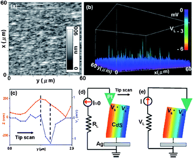 |
| | Fig. 27 (a) and (b) The topography and corresponding voltage output images of CdSnanowire arrays prepared using the PVD process, respectively. (c) Line profiles of topography (red) and output voltage (blue) scanned across CdSnanowires. (d) and (e) Contact between the AFM tip and a semiconductor CdSnanowire at two reversed local contact potentials (positive) and at two reversed local contact potentials (positive and negative), showing reverse- and forward-biased Schottky rectifying behavior, respectively. The process in (d) is to generate and preserve the charges/potential, and the process in (e) is to discharge the potential through a flow of electrons from the circuit under the driving the piezoelectric potential. Reproduced from ref. 152 with permission. Copyright © 2008, American Institute of Physics. | |
5. Conclusions and outlook
This article provides an up-to-date review of the current achievements regarding the studies of 1D CdSnanostructures, ranging from synthesis and properties to applications. Needless to say, due to the tremendous research effort and the space limitations, this article is unable to cover all the exciting works reported in this field.
The investigation of these 1D CdSnanostructures will be continuously exciting and highly rewarding, however, such nanostructures and most of their applications are still in an early stage of technical development. Undoubtedly there will be many innovations and solutions on the route towards their practical integration into nanotechnology. However, many issues need to be solved before that.
(1) Significant challenges still exist to develop a simple, efficient and cheap technology to synthesize 1D CdSnanostructures at a high quality and in large quantities; the remaining issues include but are not limited to: reliable control of diameter, length, orientation, density, crystallization and hierarchical assembly. Such a wealth of 1D CdSnanostructures could provide a playground for fundamental studies as well as for further nanoscience and nanotechnology developments.
(2) Most of the nanodevices based on single 1D CdSnanostructures are fabricated by top-down approach using a combination of lithography, etching, and deposition. Without question, this technique is complicated, time-consuming and uneconomic, thus hampering the development of practical routes. It still remains a grand challenge to develop an effective and low-cost approach to construct nanodevices with high performance characteristics.
(3) Development of techniques for the integration of 1D CdSnanostructures into nanobiosensors and chemical sensors is also required.
Acknowledgements
T. Y. Zhai thanks the Japan Society for the Promotion of Science (JSPS) for a support in the form of a fellowship tenable at the National Institute for Materials Science (NIMS), Tsukuba, Japan. This work was supported by the World Premier International Research Center (WPI) Initiative on Materials Nanoarchitectonics (MANA), MEXT, Japan. The authors are indebted for the kind permission from the corresponding publishers/authors to reproduce their materials, especially figures, used in this review.
References
- C. M. Lieber and Z. L. Wang, MRS Bull., 2007, 32, 99–104 CAS.
- X. S. Fang, Y. Bando, U. K. Gautam, T. Y. Zhai, H. B. Zeng, X. J. Xu, M. Y. Liao and D. Golberg, Crit. Rev. Solid State Mat. Sci., 2009, 34, 190–223 Search PubMed.
- D. Golberg, Y. Bando, C. C. Tang and C. Y. Zhi, Adv. Mater., 2007, 19, 2413–2432 CrossRef CAS.
- Z. J. Gu, Y. Ma, T. Y. Zhai, B. F. Gao, W. S. Yang and J. N. Yao, Chem.–Eur. J., 2006, 12, 7717–7723 CrossRef CAS.
- M. Law, J. Goldberger and P. D. Yang, Annu. Rev. Mater. Res., 2004, 34, 83–122 CrossRef CAS.
- C. N. R. Rao, R. Voggu and A. Govindaraj, Nanoscale, 2009, 1, 96–105 RSC.
- Y. N. Xia, P. D. Yang, Y. G. Sun, Y. Y. Wu, B. Mayers, B. Gates, Y. D. Yin, F. Kim and H. Q. Yan, Adv. Mater., 2003, 15, 353–389 CrossRef CAS.
-
T. Y. Zhai, X. S. Fang, H. B. Zeng, X. J. Xu, Y. Bando and D. Golberg, Pure Appl. Chem., accepted Search PubMed.
- T. Y. Zhai, X. S. Fang, Y. Bando, B. Dierre, B. D. Liu, H. B. Zeng, X. J. Xu, Y. Huang, X. L. Yuan, T. Sekiguchi and D. Golberg, Adv. Funct. Mater., 2009, 19, 2423–2430 CrossRef CAS.
- M. Zhang, T. Y. Zhai, X. Wang, Q. Liao, Y. Ma and J. N. Yao, J. Solid State Chem., 2009, 182, 3188–3194 CrossRef CAS.
- T. Y. Zhai, X. S. Fang, Y. Bando, Q. Liao, X. J. Xu, H. B. Zeng, Y. Ma, J. N. Yao and D. Golberg, ACS Nano, 2009, 3, 949–959 CrossRef CAS.
- X. F. Duan, Y. Huang, R. Agarwal and C. M. Lieber, Nature, 2003, 421, 241–245 CrossRef CAS.
- N. V. Hullavarad, S. S. Hullavarad and P. C. Karulkar, J. Nanosci. Nanotechnol., 2008, 8, 3272–3299 CrossRef CAS.
- Z. L. Wang, ACS Nano, 2008, 2, 1987–1992 CrossRef CAS.
- D. Moore and Z. L. Wang, J. Mater. Chem., 2006, 16, 3898–3905 RSC.
- X. S. Fang and L. D. Zhang, J. Mater. Sci. Technol., 2006, 22, 721–736 CAS.
- C. J. Barrelet, Y. Wu, D. C. Bell and C. M. Lieber, J. Am. Chem. Soc., 2003, 125, 11498–11499 CrossRef CAS.
- C. H. Ye, G. W. Meng, Y. H. Wang, Z. Jiang and L. D. Zhang, J. Phys. Chem. B, 2002, 106, 10338–10341 CrossRef CAS.
- T. Y. Zhai, Z. J. Gu, Y. Ma, W. S. Yang, L. Y. Zhao and J. N. Yao, Mater. Chem. Phys., 2006, 100, 281–284 CrossRef CAS.
- L. Y. Zhao, W. S. Yang, G. J. Zhang, T. Y. Zhai and J. N. Yao, Chem. Phys. Lett., 2003, 379, 479–483 CrossRef CAS.
- C. N. R. Rao and A. Govindaraj, Adv. Mater., 2009, 21, 4208–4233 CrossRef CAS.
- X. P. Shen, A. H. Yuan, F. Wang, J. M. Hong and Z. Xu, Solid State Commun., 2005, 133, 19–22 CrossRef CAS.
- L. F. Dong, J. Jiao, M. Coulter and L. Love, Chem. Phys. Lett., 2003, 376, 653–658 CrossRef CAS.
- T. Gao and T. H. Wang, J. Phys. Chem. B, 2004, 108, 20045–20049 CrossRef CAS.
- Z. L. Wang, Mater. Sci. Eng., R, 2009, 64, 33–71 CrossRef.
- J. Puthussery, A. D. Lan, T. H. Kosel and M. Kuno, ACS Nano, 2008, 2, 357–367 CrossRef CAS.
- Y. F. Lin, Y. J. Hsu, S. Y. Lu and S. C. Kung, Chem. Commun., 2006, 2391–2393 RSC.
- S. Kar and S. Chaudhuri, J. Phys. Chem. B, 2006, 110, 4542–4547 CrossRef CAS.
- Y. Z. Long, Z. J. Chen, W. L. Wang, F. L. Bai, A. Z. Jin and C. Z. Gu, Appl. Phys. Lett., 2005, 86, 153102 CrossRef.
- S. C. Yan, L. T. Sun, P. Qu, N. P. Huang, Y. C. Song and Z. D. Xiao, J. Solid State Chem., 2009, 182, 2941–2945 CrossRef CAS.
- N. Yuan, G. Cheng, Y. Q. An, Z. L. Du and S. X. Wu, Nanoscale Res. Lett., 2009, 4, 414–419 Search PubMed.
- P. Yan, Y. Xie, Y. T. Qian and X. M. Liu, Chem. Commun., 1999, 1293–1294 RSC.
- C. C. Kang, C. W. Lai, H. C. Peng, J. J. Shyue and P. T. Chou, Small, 2007, 3, 1882–1885 CrossRef CAS.
- L. F. Xi, W. X. W. Tan, K. S. Chua, C. Boothroyd and Y. M. Lam, Thin Solid Films, 2009, 517, 6430–6434 CrossRef CAS.
- H. Zhang, X. Y. Ma, J. Xu, J. J. Niu, J. Sha and D. R. Yang, J. Cryst. Growth, 2002, 246, 108–112 CrossRef CAS.
- D. S. Xu, Y. J. Xu, D. P. Chen, G. L. Guo, L. L. Gui and Y. Q. Tang, Adv. Mater., 2000, 12, 520–522 CrossRef CAS.
- D. Routkevitch, T. Bigioni, M. Moskovits and J. M. Xu, J. Phys. Chem., 1996, 100, 14037–14047 CrossRef CAS.
- J. P. Ge and Y. D. Li, Adv. Funct. Mater., 2004, 14, 157–162 CrossRef CAS.
- R. M. Ma, X. L. Wei, L. Dai, H. B. Huo and G. G. Qin, Nanotechnology, 2007, 18, 205605 CrossRef.
- X. F. Duan and C. M. Lieber, Adv. Mater., 2000, 12, 298–302 CrossRef CAS.
- A. L. Pan, D. Liu, R. B. Liu, F. F. Wang, X. Zhu and B. S. Zou, Small, 2005, 1, 980–983 CrossRef CAS.
- Y. W. Wang, G. W. Meng, L. D. Zhang, C. H. Liang and J. Zhang, Chem. Mater., 2002, 14, 1773–1777 CrossRef CAS.
- A. Datta, P. G. Chavan, F. J. Sheini, M. A. More, D. S. Joag and A. Patra, Cryst. Growth Des., 2009, 9, 4157–4162 CrossRef CAS.
- H. Pan, G. C. Xing, Z. H. Ni, W. Ji, Y. P. Feng, Z. Tang, D. H. C. Chua, J. Y. Lin and Z. X. Shen, Appl. Phys. Lett., 2007, 91, 193105 CrossRef.
- J. H. Zhan, X. G. Yang, D. W. Wang, S. D. Li, Y. Xie, Y. N. Xia and Y. T. Qian, Adv. Mater., 2000, 12, 1348–1351 CrossRef CAS.
- G. Z. Shen and C. J. Lee, Cryst. Growth Des., 2005, 5, 1085–1089 CrossRef CAS.
- Y. W. Jun, S. M. Lee, N. J. Kang and J. Cheon, J. Am. Chem. Soc., 2001, 123, 5150–5151 CrossRef CAS.
- S. Acharya, I. Patla, J. Kost, S. Efrima and Y. Golan, J. Am. Chem. Soc., 2006, 128, 9294–9295 CrossRef CAS.
- F. Chen, R. J. Zhou, L. G. Yang, M. M. Shi, G. Wu, M. Wang and H. Z. Chen, J. Phys. Chem. C, 2008, 112, 13457–13462 CrossRef CAS.
- Y. X. Li, Y. F. Hu, S. Q. Peng, G. X. Lu and S. B. Li, J. Phys. Chem. C, 2009, 113, 9352–9358 CrossRef CAS.
- A. Ghezelbash, B. Koo and B. A. Korgel, Nano Lett., 2006, 6, 1832–1836 CrossRef CAS.
- Y. J. Xiong, Y. Xie, J. Yang, R. Zhang, C. Z. Wu and G. A. Du, J. Mater. Chem., 2002, 12, 3712–3716 RSC.
- M. W. Shao, Z. C. Wu, F. Gao, Y. Ye and X. W. Wei, J. Cryst. Growth, 2004, 260, 63–66 CrossRef CAS.
- H. Zhang, X. Y. Ma, J. Xu and D. R. Yang, J. Cryst. Growth, 2004, 263, 372–376 CrossRef CAS.
- T. Y. Peng, H. P. Yang, K. Dai, X. L. Pu and K. Hirao, Chem. Phys. Lett., 2003, 379, 432–436 CrossRef CAS.
- M. W. Shao, F. Xu, Y. Y. Peng, J. Wu, Q. Li, S. Y. Zhang and Y. T. Qian, New J. Chem., 2002, 26, 1440–1442 RSC.
- Y. Y. Huang, F. Q. Sun, H. J. Wang, Y. He, L. S. Li, Z. X. Huang, Q. S. Wu and J. C. Yu, J. Mater. Chem., 2009, 19, 6901–6906 RSC.
- H. Pan, C. K. Poh, Y. W. Zhu, G. C. Xing, K. C. Chin, Y. P. Feng, J. Y. Lin, C. H. Sow, W. Ji and A. T. S. Wee, J. Phys. Chem. C, 2008, 112, 11227–11230 CrossRef CAS.
- X. Qian, H. Liu, Y. Guo, S. Zhu, Y. Song and Y. Li, Nanoscale Res. Lett., 2009, 4, 955–961 Search PubMed.
- X. M. Li, H. B. Chu and Y. Li, J. Solid State Chem., 2006, 179, 96–102 CrossRef CAS.
- Z. Q. Wang, J. F. Gong, J. H. Duan, H. B. Huang, S. G. Yang, X. N. Zhao, R. Zhang and Y. W. Du, Appl. Phys. Lett., 2006, 89, 033102 CrossRef.
- P. C. Wu, Y. Ye, T. Sun, R. M. Peng, X. N. Wen, W. J. Xu, C. Liu and L. Dai, ACS Nano, 2009, 3, 3138–3142 CrossRef CAS.
- Y. Wang, C. Y. To and D. H. L. Ng, Mater. Lett., 2006, 60, 1151–1155 CrossRef CAS.
- J. Y. Lee, D. S. Kim and J. Park, Chem. Mater., 2007, 19, 4663–4669 CrossRef CAS.
- C. Li, Z. T. Liu and Y. Yang, Nanotechnology, 2006, 17, 1851–1857 CrossRef CAS.
- G. Z. Shen, J. H. Cho, J. K. Yoo, G. C. Yi and C. J. Lee, J. Phys. Chem. B, 2005, 109, 9294–9298 CrossRef CAS.
- C. R. Wang, K. M. Ip, S. K. Hark and Q. Li, J. Appl. Phys., 2005, 97, 054303 CrossRef.
- J. Zhang, F. H. Jiang and L. D. Zhang, J. Phys. Chem. B, 2004, 108, 7002–7005 CrossRef CAS.
- P. C. Wu, Y. Ye, C. Liu, R. M. Ma, T. Sun and L. Dai, J. Mater. Chem., 2009, 19, 7296–7300 RSC.
- K. Y. Lee, J. R. Lim, H. Rho, Y. J. Choi, K. J. Choi and J. G. Park, Appl. Phys. Lett., 2007, 91, 201901 CrossRef.
- Y. K. Liu, J. A. Zapien, C. Y. Geng, Y. Y. Shan, C. S. Lee, Y. Lifshitz and S. T. Lee, Appl. Phys. Lett., 2004, 85, 3241–3243 CrossRef CAS.
- S. Kar, B. Satpati, P. V. Satyam and S. Chaudhuri, J. Phys. Chem. B, 2005, 109, 19134–19138 CrossRef CAS.
- X. Fan, M. L. Zhang, I. Shafiq, W. J. Zhang, C. S. Lee and S. T. Lee, Cryst. Growth Des., 2009, 9, 1375–1377 CrossRef CAS.
- J. S. Jie, W. J. Zhang, Y. Jiang, X. M. Meng, Y. Q. Li and S. T. Lee, Nano Lett., 2006, 6, 1887–1892 CrossRef CAS.
- X. T. Zhou, P. S. G. Kim, T. K. Sham and S. T. Lee, J. Appl. Phys., 2005, 98, 024312 CrossRef.
- J. Cao, J. Z. Sun, H. Y. Li, J. Hong and M. Wang, J. Mater. Chem., 2004, 14, 1203–1206 RSC.
- Y. J. Hsu and S. Y. Lu, Chem. Commun., 2004, 2102–2103 RSC.
- T. Y. Zhai, Z. J. Gu, H. Z. Zhong, Y. Dong, Y. Ma, H. B. Hu, Y. F. Li and J. N. Yao, Cryst. Growth Des., 2007, 7, 488–491 CrossRef CAS.
- T. Y. Zhai, H. Z. Zhong, Z. J. Gu, A. D. Peng, H. B. Fu, Y. Ma, Y. F. Li and J. N. Yao, J. Phys. Chem. C, 2007, 111, 2980–2986 CrossRef CAS.
- T. Y. Zhai, Z. J. Gu, Y. Dong, H. Z. Zhong, Y. Ma, H. B. Fu, Y. F. Li and J. N. Yao, J. Phys. Chem. C, 2007, 111, 11604–11611 CrossRef CAS.
- T. Y. Zhai, Y. Dong, Y. B. Wang, Z. W. Cao, Y. Ma, H. B. Fu and J. N. Yao, J. Solid State Chem., 2008, 181, 950–956 CrossRef CAS.
- Y. K. Liu, J. A. Zapien, Y. Y. Shan, C. Y. Geng, C. S. Lee and S. T. Lee, Adv. Mater., 2005, 17, 1372–1377 CrossRef CAS.
- T. Y. Zhai, X. Z. Zhang, W. S. Yang, Y. Ma, J. F. Wang, Z. J. Gu, D. P. Yu, H. Yang and J. N. Yao, Chem. Phys. Lett., 2006, 427, 371–374 CrossRef CAS.
- T. Y. Zhai, Z. J. Gu, W. S. Yang, X. Z. Zhang, J. Huang, Y. S. Zhao, D. P. Yu, H. B. Fu, Y. Ma and J. N. Yao, Nanotechnology, 2006, 17, 4644–4649 CrossRef CAS.
- X. Z. Zhang, T. Y. Zhai, Y. Ma, J. N. Yao and D. P. Yu, J. Electron Microsc., 2007, 57, 7–11 CrossRef.
- Y. Jung, D. K. Ko and R. Agarwal, Nano Lett., 2007, 7, 264–268 CrossRef CAS.
- Y. J. Hsu, S. Y. Lu and Y. F. Lin, Adv. Funct. Mater., 2005, 15, 1350–1357 CrossRef CAS.
- Y. X. Yin, Z. G. Jin and F. Hou, Nanotechnology, 2007, 18, 495608 CrossRef.
- X. L. Fu, L. H. Li and W. H. Tang, Solid State Commun., 2006, 138, 139–142 CrossRef CAS.
- M. R. Kim, Y. M. Kang and D. J. Jang, J. Phys. Chem. C, 2007, 111, 18507–18511 CrossRef CAS.
- Y. Xie, P. Yan, J. Lu, Y. T. Qian and S. Y. Zhang, Chem. Commun., 1999, 1969–1970 RSC.
- H. L. Peng, C. Xie, D. T. Schoen, K. Mcllwrath, X. F. Zhang and Y. Cui, Nano Lett., 2007, 7, 3734–3738 CrossRef CAS.
- Y. Tak, S. J. Hong, J. S. Lee and K. Yong, J. Mater. Chem., 2009, 19, 5945–5951 RSC.
- K. Das and S. K. De, J. Phys. Chem. C, 2009, 113, 3494–3501 CrossRef CAS.
- Z. Zanolli, B. A. Wacaser, M. E. Pistol, K. Deppert and L. Samuelson, J. Phys.: Condens. Matter, 2007, 19, 295218 CrossRef.
- J. Q. Hu, H. Jiang, Z. G. Chen, Y. G. Sun, Y. Bando, T. Sekiguchi and D. Golberg, J. Mater. Chem., 2009, 19, 1093–1097 RSC.
- Y. J. Choi, I. S. Hwang, J. H. Park, S. Nakm and J. G. Park, Nanotechnology, 2006, 17, 3775–3778 CrossRef CAS.
- A. L. Pan, R. B. Liu, F. F. Wang, S. S. Xie, B. S. Zou, M. Zacharias and Z. L. Wang, J. Phys. Chem. B, 2006, 110, 22313–22317 CrossRef CAS.
- C. Yang, X. C. Zhou, L. Y. Wang, X. K. Tian, Y. X. Wang and Z. B. Pi, J. Mater. Sci., 2009, 44, 3015–3019 CrossRef CAS.
- W. Y. Cheng, W. T. Chen, Y. J. Hsu and S. Y. Lu, J. Phys. Chem. C, 2009, 113, 17342–17346 CrossRef CAS.
- S. Biswas, S. Kar, S. Santra, Y. Jompol, M. Arif and S. I. Khondaker, J. Phys. Chem. C, 2009, 113, 3617–3624 CrossRef CAS.
- D. C. Yang, G. W. Meng, F. M. Han and L. D. Zhang, Mater. Lett., 2008, 62, 3213–3216 CrossRef CAS.
- F. M. Han, G. W. Meng, X. L. Zhao, Q. L. Xu, J. X. Liu, B. S. Chen, X. G. Zhu and M. G. Kong, Mater. Lett., 2009, 63, 2249–2252 CrossRef CAS.
- Y.
Q. Li, J. X. Tang, H. Wang, J. A. Zapien, Y. Y. Shan and S. T. Lee, Appl. Phys. Lett., 2007, 90, 093127 CrossRef.
- W. C. Zhou, A. L. Pan, Y. Li, G. Z. Dai, Q. Wan, Q. L. Zhang and B. S. Zou, J. Phys. Chem. C, 2008, 112, 9253–9260 CrossRef CAS.
- F. Gao and Q. Y. Lu, Nanoscale Res. Lett., 2009, 4, 371–376 Search PubMed.
- G. Z. Dai, Z. W. Peng, Q. L. Zhang, W. C. Zhou, M. X. Xia, H. X. Li, A. L. Pan, Q. Wan and B. S. Zou, Nanotechnology, 2009, 20, 125601 CrossRef.
- L. Spanhel, M. Haase, H. Weller and A. Henglein, J. Am. Chem. Soc., 1987, 109, 5649–5655 CrossRef CAS.
- F. Gao, Q. Y. Lu, S. H. Xie and D. Y. Zhao, Adv. Mater., 2002, 14, 1537–1540 CrossRef CAS.
- U. K. Gautam, L. S. Panchakarla, B. Dierre, X. S. Fang, Y. Bando, T. Sekiguchi, A. Govindaraj, D. Golberg and C. N. R. Rao, Adv. Funct. Mater., 2009, 19, 131–140 CrossRef CAS.
- X. S. Fang, U. K. Gautam, Y. Bando, B. Dierre, T. Sekiguchi and D. Golberg, J. Phys. Chem. C, 2008, 112, 4735–4742 CrossRef CAS.
- M. H. Huang, S. Mao, H. Feick, H. Q. Yan, Y. Y. Wu, H. Kind, E. Weber, R. Russo and P. D. Yang, Science, 2001, 292, 1897–1899 CrossRef CAS.
- Y. Huang, X. F. Duan and C. M. Lieber, Small, 2005, 1, 142–147 CrossRef CAS.
- M. Law, D. J. Sirbuly, J. C. Johnson, J. Goldberger, R. J. Saykally and P. D. Yang, Science, 2004, 305, 1269–1273 CrossRef CAS.
- C. J. Barrelet, A. B. Greytak and C. M. Lieber, Nano Lett., 2004, 4, 1981–1985 CrossRef CAS.
- A. B. Greytak, C. J. Barrelet, Y. Li and C. M. Lieber, Appl. Phys. Lett., 2005, 87, 151103 CrossRef.
- M. M. Richter, Chem. Rev., 2004, 104, 3003–3036 CrossRef CAS.
- C. Z. Wang, Y. F. E, L. Z. Fan, Z. H. Wang, H. B. Liu, Y. L. Li, S. H. Yang and Y. L. Li, Adv. Mater., 2007, 19, 3677–3681 CrossRef CAS.
- J. J. Miao, T. Ren, L. Dong, J. J. Zhu and H. Y. Chen, Small, 2005, 1, 802–805 CrossRef CAS.
- J. C. Lee, T. G. Kim, W. Lee, S. H. Han and Y. M. Sung, Cryst. Growth Des., 2009, 9, 4519–4523 CrossRef CAS.
- Z. Y. Fan, H. Razavi, J. Do, A. Moriwaki, O. Ergen, Y. Chueh, P. W. Leu, J. C. Ho, T. Takahashi, L. A. Reichertz, S. Neale, K. Yu, M. Wu, J. W. Ager and A. Javey, Nat. Mater., 2009, 8, 648–653 CrossRef CAS.
- E. C. Garnett and P. D. Yang, J. Am. Chem. Soc., 2008, 130, 9224–9225 CrossRef CAS.
- J. A. Czaban, D. A. Thompson and R. R. LaPierre, Nano Lett., 2009, 9, 148–154 CrossRef CAS.
- R. M. Ma, L. Dai, H. B. Huo, W. Q. Yang, G. G. Qin, P. H. Tan, C. H. Huang and J. Zheng, Appl. Phys. Lett., 2006, 89, 203120 CrossRef.
- R. M. Ma, L. Dai and G. G. Qin, Nano Lett., 2007, 7, 868–873 CrossRef CAS.
- R. M. Ma, L. Dai and G. G. Qin, Appl. Phys. Lett., 2007, 90, 093109 CrossRef.
- Y. Ye, L. Dai, P. C. Wu, C. Liu, T. Sun, R. M. Ma and G. G. Qin, Nanotechnology, 2009, 20, 375202 CrossRef CAS.
- J. G. Lu, P. C. Chang and Z. Y. Fan, Mater. Sci. Eng., R, 2006, 52, 49–91 CrossRef.
- R. M. Ma, L. Dai, H. B. Huo, W. J. Xu and G. G. Qin, Nano Lett., 2007, 7, 3300–3304 CrossRef CAS.
- L. Liao, B. Yan, Y. F. Hao, G. Z. Xing, J. P. Liu, B. C. Zhao, Z. X. Shen, Y. Wu, L. Wang, J. T. L. Thong, C. M. Li, W. Huang and T. Yu, Appl. Phys. Lett., 2009, 94, 113106 CrossRef.
- D. D. Lin, H. Wu and W. Pan, Adv. Mater., 2007, 19, 3968–3972 CrossRef CAS.
- T. Y. Zhai, X. S. Fang, M. Y. Liao, X. J. Xu, H. B. Zeng, Y. Bando and D. Golberg, Sensors, 2009, 9, 6504–6529 CrossRef CAS.
- Y. Jiang, W. J. Zhang, J. S. Jie, X. M. Meng, X. Fan and S. T. Lee, Adv. Funct. Mater., 2007, 17, 1795–1800 CrossRef CAS.
- T. Y. Zhai, H. M. Liu, H. Q. Li, X. S. Fang, M. Y. Liao, L. Li, H. S. Zhou, Y. Koide, Y. Bando and D. Golberg, Adv. Mater., 2010 DOI:10.1002/adma.200903586.
- X. S. Fang, S. L. Xiong, T. Y. Zhai, Y. Bando, M. Y. Liao, U. K. Gautam, Y. Koide, X. G. Zhang, Y. T. Qian and D. Golberg, Adv. Mater., 2009, 21, 5016–5021 CrossRef CAS.
- X. S. Fang, Y. Bando, M. Y. Liao, U. K. Gautam, C. Y. Zhi, B. Dierre, B. D. Liu, T. Y. Zhai, T. Sekiguchi, Y. Koide and D. Golberg, Adv. Mater., 2009, 21, 2034–2039 CrossRef CAS.
- X. S. Fang, Y. Bando, M. Y. Liao, T. Y. Zhai, U. K. Gautam, L. Li, Y. Koide and D. Golberg, Adv. Funct. Mater., 2010 DOI:10.1002/adfm.200901878.
- T. Gao, Q. H. Li and T. H. Wang, Appl. Phys. Lett., 2005, 86, 173105 CrossRef.
- S. P. Mondal and S. K. Ray, Appl. Phys. Lett., 2009, 94, 223119 CrossRef.
- Y. K. Liu, X. P. Zhou, D. D. Hou and H. Wu, J. Mater. Sci., 2006, 41, 6492–6496 CrossRef CAS.
- J. S. Jie, W. J. Zhang, Y. Jiang and S. T. Lee, Appl. Phys. Lett., 2006, 89, 223117 CrossRef.
- Q. H. Li, T. Gao and T. H. Wang, Appl. Phys. Lett., 2005, 86, 193109 CrossRef.
- T. Hirai, Y. Bando and I. Komasawa, J. Phys. Chem. B, 2002, 106, 8967–8970 CrossRef CAS.
- Y. Guo, H. Zhang, Y. Wang, Z. L. Liao, G. D. Li and J. S. Chen, J. Phys. Chem. B, 2005, 109, 21602–21607 CrossRef CAS.
- W. T. Yao, S. H. Yu, S. J. Liu, J. P. Chen, X. M. Liu and F. Q. Li, J. Phys. Chem. B, 2006, 110, 11704–11710 CrossRef CAS.
- L. Li, X. S. Fang, H. G. Chew, F. Zheng, T. H. Liew, X. J. Xu, Y. X. Zhang, S. S. Pan, G. H. Li and L. D. Zhang, Adv. Funct. Mater., 2008, 18, 1080–1088 CrossRef CAS.
- L. Li, X. J. Hu, H. G. Chew, X. H. Huang, X. C. Dou, S. S. Pan, G. H. Li and L. D. Zhang, J. Phys. Chem. C, 2008, 112, 5328–5332 CrossRef CAS.
- X. S. Fang, Y. Bando, U. K. Gautam, C. H. Ye and D. Golberg, J. Mater. Chem., 2008, 18, 509–522 RSC.
- G. Z. Shen, P. C. Chen, K. Ryu and C. W. Zhou, J. Mater. Chem., 2009, 19, 828–839 RSC.
- C. H. Ye, Y. Bando, X. S. Fang, G. Z. Shen and D. Golberg, J. Phys. Chem. C, 2007, 111, 12673–12676 CrossRef CAS.
- Z. L. Wang and J. H. Song, Science, 2006, 312, 242–246 CrossRef CAS.
- Y. F. Lin, J. H. Song, Y. Ding, S. Y. Lu and Z. L. Wang, Appl. Phys. Lett., 2008, 92, 022105 CrossRef.
- Y. F. Lin, J. H. Song, Y. Ding, S. Y. Lu and Z. L. Wang, Adv. Mater., 2008, 20, 3127–3130 CrossRef CAS.
|
| This journal is © The Royal Society of Chemistry 2010 |
Click here to see how this site uses Cookies. View our privacy policy here.