Lateral engineering of surface states – towards surface-state nanoelectronics
F. J.
García de Abajo
*a,
J.
Cordón
b,
M.
Corso
c,
F.
Schiller
d and
J. E.
Ortega
*bcd
aInstituto de Óptica - CSIC, Serrano 121, 28006 Madrid, Spain. E-mail: jga@cfmac.csic.es
bDepartamento de Física Aplicada I, Plaza de Oñate 2, 20018 San Sebastián, Spain. E-mail: enrique.ortega@ehu.es
cDonostia International Physics Center, Manuel de Lardizábal 3, 20018 San Sebastián, Spain
dCentro de Física de Materiales (CSIC-UPV/EHU)-Materials Physics Center (MPC), Manuel de Lardizábal 4, 20018 San Sebastián, Spain
First published on 9th April 2010
Abstract
Patterned metal surfaces can host electron quantum waves that display interference phenomena over distances of a few nanometres, thus providing excellent information carriers for future atomic-scale devices. Here we demonstrate that collimation and waveguiding of surface electrons can be realized in silver-induced strain dislocation networks on Cu(111) surfaces, as a conceptual proof-of-principle of surface-state nanoelectronics (SSNE). The Ag/Cu(111) system exhibits featured surface bands with gaps at the Fermi energy, which are basic requirements for a potential SSNE material. We establish a solid analogy between the behavior of surface-state electrons and surface plasmons in patterned metal surfaces, thus facilitating the transfer of existing knowledge on plasmonic structures to the new scenario presented by engineered electronic surface-state nanostructures, with the advantage of a 1000-fold reduction in wavelength and geometrical parameters.
The search for information carriers that can be manipulated increasingly faster over smaller length scales is rapidly evolving from electrons and microelectronics towards photons and nanophotonics.1 In particular, optical excitations trapped in metal–dielectric interfaces (surface plasmons) allow subwavelength control of light-energy flow through structures containing sub-micron elemental units, the design of which has emerged as the field of plasmonics.2,3 Plasmons can be filtered and guided in metallic stripes2 and they can be manipulated through periodic patterning of metallic surfaces.4 Likewise, electrons trapped in surface states of noble metals exhibit free-particle motion parallel to the surface, and they can be scattered by atomic defects (e.g., steps), thus becoming laterally confined within quantum corrals and other truly nanometre-scale structures.5 Close to the Fermi level, electrons and holes in surface states have wavelengths in the range of the nanometre and maintain their coherence over significantly larger propagation distances.6 These features reveal surface electrons as excellent information carriers for a new signal-processing technology.
Adsorbed atoms, lattice vacancies, and surface steps act as repulsive scattering centers for surface electrons in noble metals.5–8 Surface-state bands can thus be engineered using these elements, arranged on atomic scales by STM manipulation7,8 or by self-assembly5 to, for example, achieve focusing via atom-based mirrors9 and buried interfaces.10 In a related development, graphene has been the subject of intense scrutiny in recent years because of its ability to scatter and interfere surface states,11 leading to extraordinary effects such as negative refraction.12 However, self-assembly is particularly attractive to produce massive, periodic nanopatterning with lattice constants in the range of the electron Fermi wavelength (∼1 nm). This is the case of the triangular misfit dislocation network formed by coating Cu(111) with one monolayer of silver,13,14 which we use here to establish some relevant building blocks of surface-state nanoelectronics (SSNE).
Fig. 1 illustrates our vision of a SSNE device consisting of an electron injected into a channel of missing triangles embedded in a textured silver-covered Cu(111) surface. The electron energy is chosen to lie in an absolute band gap of the triangle lattice, just 19 meV above the Fermi level. Similar to photons guided in photonic crystals,15 the electron is guided around a 60° corner because it cannot propagate outside the channel. Both the flat channel and the triangular structure are the low- and high-temperature phases of the Ag/Cu(111) system (i.e., the Moiré and the triangular strain dislocation network, respectively), which have been shown to coexist at intermediate temperatures.13 Patterning of such a waveguide channel would be possible using a local heating probe (e.g., a STM tip). Next, we discuss some relevant details of the analysis leading to this concept.
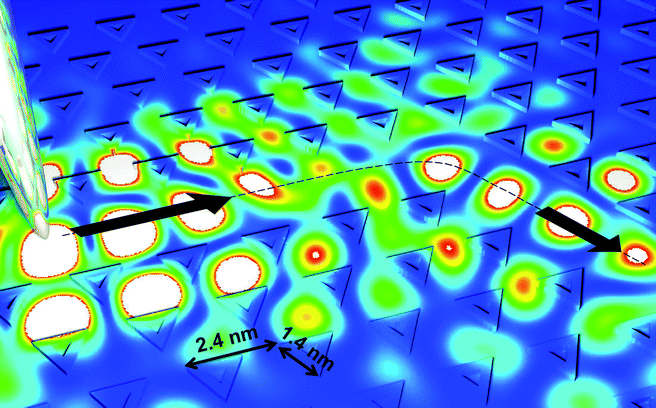 | ||
| Fig. 1 Waveguiding and bending of electronic surface states (EESs). A missing row in a periodic array of triangular surface defects defines a waveguide for surface electrons, injected from a metallic tip at the desired location, and confined to propagate along the bending guide by a bandgap in the periodic structure. The image shows an array of triangular defects formed by depositing one monolayer of silver on a Cu(111) surface, alongside the density of an electron wave launched from a point-like source (the tip) with an energy of 19 meV above the Fermi level. | ||
Surface electrons and plasmons evolving on flat surfaces are governed by the same wave equation
| (∇2 + k2)ϕ = 0 , | (1) |
| (∇2 + k2 − 2meffV)ϕ = 0 , | (2) |
| ε = 1 − 2meffV/k2 , |
Plasmons display wavelengths in the range of the micron in practical applications,2,4 whereas electron surface states (ESSs) near the Fermi level have a wavelength of 3.7 nm in Cu(111) and similar values in other noble metal surfaces. Consequently, the ability of surface plasmons to encode and process information can be imitated by ESSs, only on a much shorter length scale and with slightly faster response times. For example, a plasmon of 1.5 μm wavelength takes ∼5 fs to travel across one wavelength, which has to be compared with ∼2 fs for an ESS to move along the Fermi-wavelength distance.
The STM picture in Fig. 2(a) shows a hexagonal superlattice of triangular dislocations (2.43 nm lattice constant) within a long Ag layer nanostripe grown on Cu(111). Such a monolayer-thick nanostripe is an important element to achieve surface electron focusing, as we show in Fig. 3. Ag nanostripes are spontaneously formed after low-temperature evaporation and mild annealing of Ag on Cu(111).13,17 The inset sketches the atomic arrangement of a single triangular defect. It consists of a dislocation loop in the topmost atomic layer of the Cu substrate plane, arising after removal of five Cu atoms and displacement of another 10 Cu atoms to hcp positions.13 On top, Ag atoms form a defect-free close-packed layer.
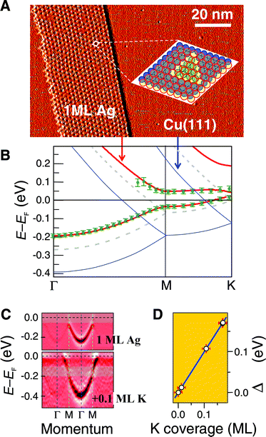 | ||
| Fig. 2 Surface band transformation of Cu(111) by Ag-induced dislocation networks and potassium doping. (a) Ag nanostripe attached to a Cu(111) surface step, featuring a characteristic array of triangular misfit dislocations. The dislocations involve removal of five topmost copper atoms (blue circles in the inset) and shifting of ten copper atoms inside the triangle (green circles), avoiding on-top positions of silver atoms (open red circles). (b) Surface bands for clean Cu(111) (blue), the Ag monolayer without triangular dislocations (low-temperature Moiré, dotted), and with triangles (300 K, red). For the latter, the band structure is obtained from a simple model calculation (curves) that fits photoemission data at 300 K (symbols). (c) Surface bands measured with angle-resolved photoemission in the Ag/Cu(111) monolayer (top) and after adding 0.1 monolayers of potassium (bottom). The latter changes the surface chemical potential (i.e., the Fermi level position). (d) Measured Fermi-level shift as a function of potassium coverage. | ||
![Collimation of surface states by the triangular-lattice nanostripe of Fig. 2(a). (a) A point source (⊗ symbol) similar to the tip of Fig. 1 injects an electron (600 meV relative to the bare-copper surface-band bottom) that is collimated after transmission through a lattice stripe [similar to the one in Fig. 2(a)]. (b) Ray picture sketch, showing that collimation in (a) is produced by coupling of the injected circular wave (red circle in parallel-momentum space) to relatively flat bands of the surface-state superlattice. The surface bands of both the bare Cu(111) (red semicircle) and the Ag/Cu(111) crystal (black curves) are shown at the energy of the injected electron. The background density plot (white-blue scale) represents the angle-resolved intensity of photoemission from the corrugated surface.](/image/article/2010/NR/b9nr00386j/b9nr00386j-f3.gif) | ||
| Fig. 3 Collimation of surface states by the triangular-lattice nanostripe of Fig. 2(a). (a) A point source (⊗ symbol) similar to the tip of Fig. 1 injects an electron (600 meV relative to the bare-copper surface-band bottom) that is collimated after transmission through a lattice stripe [similar to the one in Fig. 2(a)]. (b) Ray picture sketch, showing that collimation in (a) is produced by coupling of the injected circular wave (red circle in parallel-momentum space) to relatively flat bands of the surface-state superlattice. The surface bands of both the bare Cu(111) (red semicircle) and the Ag/Cu(111) crystal (black curves) are shown at the energy of the injected electron. The background density plot (white-blue scale) represents the angle-resolved intensity of photoemission from the corrugated surface. | ||
The Ag evaporation and the formation of the triangle lattice leads to a profound transformation of the surface band structure.13,14,18,19Fig. 2(b) shows the measured band structure (symbols) compared to the calculated free-electron-like bands of both the Cu(111) surface (blue curves) and the low-temperature Ag/Cu(111) Moiré phase (dashed curves), as well as the strongly featured bands of the Ag/Cu(111) triangular dislocation lattice (red curves), formed by annealing the Moiré phase at 300 K. The latter is calculated by modeling the corrugated (triangle lattice) Ag/Cu(111) nanostripe through eqn (2), assuming the origin of V at the bottom of an uncorrugated (Moiré) Ag/Cu(111) surface band,13,18 and defining open triangular regions coinciding with the dislocation loops, in which the potential is 650 meV higher. This is the only adjustable parameter in the model, describing a barrier strength similar to monatomic step edges.17 We have solved eqn (2) using plane-wave expansions for an infinitely-extended triangular lattice. The excellent agreement between experiment (symbols) and theory clearly indicates the validity of the level of description provided by eqn (2). We observe that superlattice bands in the Ag nanostripe [red lines in Fig. 2(b)] deviate notably from free electrons in both the Ag/Cu(111) Moiré (dashed curves) and the Cu(111) (blue curves), in particular around the Fermi energy, where an absolute gap opens up (25 meV wide at ![[K with combining macron]](https://www.rsc.org/images/entities/i_char_004b_0304.gif) ).
).
Efficient information carriers must maintain coherence over large distances. In surface electrons, this is only achieved near the Fermi energy (E ∼ EF), where the hole or electron mean free path diverges as (E − EF)−2.20 However, surface nanoelectronics phenomena are associated to specific energies in the superlattice band structure, and hence large (nominally infinite) coherence lengths require EF positioning (for example, at gap energies in waveguiding). Strictly speaking, since the Fermi energy in metals is fixed by bulk states, the tunable parameter is the chemical potential of the surface. Changing the crystal temperature allows a controllable 50 meV upwards shift of EF in noble metals,14 which is enough to reach the gap in the Ag/Cu(111) system, thereby enabling waveguiding with a nominally infinite electron coherence length. Doping with potassium results in even larger shifts of EF in noble metal surfaces.21Fig. 2(c) and 2(d) prove that in fact the K-induced rigid surface band shift also occurs in the Ag/Cu(111) dislocation network. In Fig. 2(c) we display the photoemission intensity map along the ![[capital Gamma, Greek, macron]](https://www.rsc.org/images/entities/i_char_e0ba.gif)
![[M with combining macron]](https://www.rsc.org/images/entities/i_char_004d_0304.gif) direction for 1 ML Ag/Cu(111), before and after K evaporation. The angle-resolved photoemission experiments (25 meV and 0.15° energy and angular resolutions, respectively) were carried out using 67 eV photons at the PGM beam line of the Synchrotron Radiation Center (SRC) in Stoughton (Wisconsin). After adding 0.1 ML of K, the gap near the point of the first Brillouin zone, which straddles EF in the undoped system [Fig. 2(b)], is entirely brought below the Fermi energy, without affecting the band topology. As shown in Fig. 2(d), such a downwards band shift is proportional to K coverage, with an ∼ 0.1 ML:0.1 eV ratio, as also observed in bare Cu(111) surfaces.21 Therefore, doping can allow us to situate the desired portion of electron or hole bands near the Fermi energy, in which they can propagate long distances with minimum inelastic attenuation.22
direction for 1 ML Ag/Cu(111), before and after K evaporation. The angle-resolved photoemission experiments (25 meV and 0.15° energy and angular resolutions, respectively) were carried out using 67 eV photons at the PGM beam line of the Synchrotron Radiation Center (SRC) in Stoughton (Wisconsin). After adding 0.1 ML of K, the gap near the point of the first Brillouin zone, which straddles EF in the undoped system [Fig. 2(b)], is entirely brought below the Fermi energy, without affecting the band topology. As shown in Fig. 2(d), such a downwards band shift is proportional to K coverage, with an ∼ 0.1 ML:0.1 eV ratio, as also observed in bare Cu(111) surfaces.21 Therefore, doping can allow us to situate the desired portion of electron or hole bands near the Fermi energy, in which they can propagate long distances with minimum inelastic attenuation.22
By analogy to plasmonics, we anticipate that collimation, focusing, waveguiding, and energy-filtering of ESSs can provide the basic building blocks of future SSNE devices. As examples, we discuss waveguiding in a Ag channel with missing triangles (Fig. 1) and collimation through a Ag nanostripe (Fig. 3). Both missing triangles and nanostripes can indeed be found in the Ag/Cu(111) system.13 Since translational invariance is broken in these systems, we apply real-space discretization for their simulation. Figs. 1 and 3 present surface-state wave functions obtained by solving eqn (2) with a boundary element method approach (BEM), which is very reliable for large, finite structures, by analogy to similar methods employed in the solution of Maxwell's equations.23,24 It applies to situations in which the potential V takes uniform values inside each homogeneous region of a set that tessellates the surface plane, with the boundaries between different regions considered to be abrupt. We can then express the wave function inside region j of potential Vj in terms of auxiliary boundary sources σj as
 | (3) |
| (∇2 + k2 − 2meffVj)Gj(R) = −δ(R) . |
| Gj(R) = (−imeff/2)H(1)0 (kjR) , |
 is the local electron wavevector and H(1)0 is a Hankel function. By construction, eqn (3) satisfies eqn (2) inside region j, but the boundary conditions at the interfaces have to be taken care of. In BEM, the contour integrals are discretized through a set of representative points (e.g., equally spaced points in the triangles), so that two unknown variables are defined for each of them (the value of σj on either side of the interface), which are determined upon application of the continuity of both the wave function and its derivative along the boundary normal. This results in a set of linear equations that are solved by direct matrix inversion. We have obtained converged results using ∼50 points per triangle. Finally, the electron is considered to originate in a point source at R0, simply given by ϕext(R) = Gj0(R − R0) in the region j0 where R0 is placed (and zero elsewhere). In practical terms, the source could be provided by a STM tip.
The waveguiding effect in Fig. 1 takes place because the electron energy lies in the absolute gap of the triangle lattice. In contrast, the collimation in Fig. 3(a) requires a more sophisticated use of the band structure, as illustrated in Fig. 3(b): (i) the injected electron, propagating in flat Cu(111), corresponds to a circle in parallel wavevector space; (ii) the component of momentum along the direction parallel to the 2D triangle-lattice stripe must be conserved, thus providing selective access to specific regions of the crystal band structure [Fig. 3(b), thick solid curves]; (iii) the new direction of propagation must be along the group velocity in these bands (see arrows), which results in collimation along the stripe normal in Fig. 3. Thus, the collimation effect arises as a result of electron momentum conservation parallel to the stripe direction, which places the electron into flat bands with group velocity along the stripe normal.
Surface nanoelectronic devices, such as the waveguide and the focusing nanostripe, involve interfaces that separate different propagating media. For Fermi-energy electrons with nominally infinite propagation length, interface scattering may become a source of surface beam decoherence and damping. The latter is generally high for atomic steps, but minimum in the case of Ag.25 The focusing effect in Fig. 3 involves surface state scattering at a Ag-decorated Cu step and at a free Ag monolayer edge. Both interfaces give rise to negligible inelastic scattering of surface states.17 In the waveguide of Fig. 1, the wall of the conducting channel is not a physical step, but a surface potential discontinuity from the Ag Moiré (channel) to the triangular lattice (gapped medium). This is similar to the case of lateral NaCl/Cu(111) and vacuum/Cu(111) interfaces, in which surface electron waves visibly undergo coherent reflection and refraction.26 Additionally, K doping enhances inelastic scattering in propagating media. This effect may reduce beam transmission across the focusing Ag nanostripe, although it would not affect the surface state waveguide.22
Information processing via SSNE will require a suite of tools that are capable of manipulating surface electrons at will. The effective potential model discussed above provides a versatile, reliable method for simulating possible useful structures, as indicated by the reported agreement between measured and modeled bands in the Ag/Cu(111) triangle lattice. In particular, we have shown that waveguiding and collimation of surface states is possible in such lattice. The analogy that we have established between these states and plasmons facilitates the extrapolation of studies such as reflection27 and negative refraction28 of plasmons towards similar goals using surface states.
Acknowledgements
This work was supported in part by the Spanish MICINN (MAT2007-66050, MAT2007-63083, and Consolider NanoLight.es), the EU (NMP4-SL-2008-213669-ENSEMBLE), the Basque Government (IT-257-07), and the University of the Basque Country (GIU06/27). The SRC is funded by the National Science Foundation (Award No. DMR-0084402).Notes and references
- R. Zia, J. A. Schuller, A. Chandran and M. L. Brongersma, Mater. Today, 2006, 9, 20–27 CrossRef CAS.
- W. L. Barnes, A. Dereux and T. W. Ebbesen, Nature, 2003, 424, 824–830 CrossRef CAS.
- E. Ozbay, Science, 2006, 311, 189–193 CrossRef CAS.
- S. I. Bozhevolnyi, J. Erland, K. Leosson, P. M. W. Skovgaard and J. M. Hvam, Phys. Rev. Lett., 2001, 86, 3008–3011 CrossRef CAS.
- C. Didiot, S. Pons, B. Kierren, Y. Fagot-Revurat and D. Malterre, Nat. Nanotechnol., 2007, 2, 617–621 CrossRef CAS.
- O. Jeandupeux, L. Bürgi, A. Hirstein, H. Brune and K. Kern, Phys. Rev. B: Condens. Matter Mater. Phys., 1999, 59, 15926–15934 CrossRef CAS.
- M. F. Crommie, C. P. Lutz and D. M. Eigler, Nature, 1993, 363, 524–527 CrossRef CAS.
- M. F. Crommie, C. P. Lutz and D. M. Eigler, Science, 1993, 262, 218–220 CrossRef CAS.
- M. Sentef, A. P. Kampf, S. Hembacher and J. Mannhart, Phys. Rev. B: Condens. Matter Mater. Phys., 2006, 74, 153407 CrossRef.
- A. Weismann, M. Wenderoth, S. Lounis, P. Zahn, N. Quaas, R. G. Ulbrich, P. H. Dederichs and S. Blügel, Science, 2009, 323, 1190–1193 CrossRef CAS.
- G. M. Rutter, J. N. Crain, N. P. Guisinger, T. Li, P. N. First and J. A. Stroscio, Science, 2007, 317, 219–222 CrossRef CAS.
- V. V. Cheianov, V. Fal'ko and B. L. Altshuler, Science, 2007, 315, 1252–1255 CrossRef CAS.
- A. Bendounan, H. Cercellier, Y. Fagot-Revurat, B. Kierren, V. Y. Yurov and D. Malterre, Phys. Rev. B: Condens. Matter Mater. Phys., 2003, 67, 165412 CrossRef.
- F. Schiller, J. Cordón, D. V. A. Rubio and J. E. Ortega, Phys. Rev. Lett., 2005, 94, 016103 CrossRef CAS.
- J. D. Joannopoulos, R. D. Meade and J. N. Winn, Photonic Crystals: Molding the Flow of Light, Princeton University Press, Singapore, 1995 Search PubMed.
- A. Mugarza, J. E. Ortega, F. J. Himpsel and F. J. García de Abajo, Phys. Rev. B: Condens. Matter Mater. Phys., 2003, 67, 081404 CrossRef.
- F. Schiller, M. Ruiz-Osés, J. Cordón and J. E. Ortega, Phys. Rev. Lett., 2005, 95, 066805 CrossRef CAS.
- A. Bendounan, F. Forster, J. Ziroff, F. Schmitt and F. Reinert, Phys. Rev. B: Condens. Matter Mater. Phys., 2005, 72, 075407 CrossRef.
- A. Bendounan, F. Forster, F. Reinert, B. Kierren, Y. Fagot-Revurat and D. Malterre, Phys. Rev. Lett., 2006, 96, 029701 CrossRef CAS.
- D. Pines and P. Nozières, The Theory of Quantum Liquids, W. A. Benjamin Inc., New York, 1966 Search PubMed.
- F. Schiller, M. Corso, M. Urdanpilleta, T. Ohta, A. Bostwick, J. L. McChesney, E. Rotenberg and J. E. Ortega, Phys. Rev. B: Condens. Matter Mater. Phys., 2008, 77, 153410 CrossRef.
- K doping can be used to shift the gap of the triangular structure to EF, but the conducting channel would remain undoped. This is important to avoid inelastic attenuation in the waveguide. For the focusing device in Fig. 3, a minimum of 0.15 ML of K may be required in order to offset nanostripe bands. From the surface state linewidth analysis, we estimate an inelastic scattering length at EF of ∼ 10 nm for 0.15 ML K/Ag/Cu(111). Such length is of the order of the nanostripe width, which therefore transmits at least 40% of the incident beam.
- F. J. García de Abajo and A. Howie, Phys. Rev. Lett., 1998, 80, 5180–5183 CrossRef CAS.
- V. Myroshnychenko, J. Rodríguez-Fernández, I. Pastoriza-Santos, A. M. Funston, C. Novo, P. Mulvaney, L. M. Liz-Marzán and F. J. García de Abajo, Chem. Soc. Rev., 2008, 37, 1792–1805 RSC.
- H. Jensen, J. Kröger, R. Berndt and S. Crampin, Phys. Rev. B: Condens. Matter Mater. Phys., 2005, 71, 155417 CrossRef.
- J. Repp, G. Meyer and K. H. Rieder, Phys. Rev. Lett., 2004, 92, 036803 CrossRef.
- M. U. González, J. C. Weeber, A. L. Baudrion, A. Dereux, A. L. Stepanov, J. R. Krenn, E. Devaux and T. W. Ebbesen, Phys. Rev. B: Condens. Matter Mater. Phys., 2006, 73, 155416 CrossRef.
- H. J. Lezec, J. A. Dionne and H. A. Atwater, Science, 2007, 316, 430–432 CrossRef CAS.
| This journal is © The Royal Society of Chemistry 2010 |