Bidirectional mediation of TiO2 nanowires field effect transistor by dipole moment from purple membrane
Rui
Li
ab,
Ye
Gan
ab,
Qun Liang
Song
ab,
Zhi Hong
Zhu
ab,
Jingsheng
Shi
ab,
Hongbin
Yang
ab,
Wei
Wang
ab,
Peng
Chen
a and
Chang Ming
Li
*ab
aSchool of Chemical and Biomedical Engineering, Nanyang Technological University, 70 Nanyang Drive, Singapore 637457, Singapore. E-mail: ECMLi@ntu.edu.sg; Fax: +65 6791 1761; Tel: +65 6790 4485
bCenter for Advanced Bionanosystems, Nanyang Technological University, 70 Nanyang Drive, Singapore 637457, Singapore
First published on 8th June 2010
Abstract
Bacteriorhodopsin-embedded purple membrane (bR-PM) is one of the most promising biomaterials for various bioelectronics applications. In this work, we demonstrate that a dipole bio-originated from bR-PM can bidirectionally mediate the performance of a bottom-contact TiO2 nanowire field effect transistor (FET) for performance improvement. When negative gate voltage is applied, both transfer and output characteristics of the TiO2 nanowire FET are enhanced by the bR-PM modification, resulting in a hole mobility increased by a factor of 2. The effect of the number of the deposited bR-PM layers on the normalized ΔID of the FET suggests that the additional electric field generated by the dipole moment natively existing in bR-PM actually boosts the performance of the TiO2 nanowires FET.
Introduction
One-dimensional (1D) inorganic nanostructures (nanotubes, nanowires and nanorods) are of great importance in both theoretical study1 and practical applications2 because they possess unique physical and chemical properties derived from various sizes, shapes and constitutions. Currently, the study of metal oxide semiconductors with 1D nanostructures intrigues many research groups, particularly due to their potential applications in electronic and optoelectronic devices, such as solar cells,3 nanosensors4 and nanolasers.5 Among numerous materials in this category, TiO2 nanostructures have been extensively studied in electrochemical sensors,6 photovoltaic cells7 and lithium batteries.8 Besides their inherent physicochemical properties, TiO2 nanostructures have low toxicity and high biocompatibility,9 which make them an exceptional candidate especially for uses associated with biomaterials.10 To date, only a few demonstrations of TiO2 nanowires-based field effect transistors (FETs), including single nanowire FET11 and Co-doped TiO2 nanowires FET,12 have been reported. However, it remains a great challenge to improve the charge transport properties, particularly by an external mediation in the electrical transport of the TiO2 nanowires FET.Bacteriorhodopsin (bR), a unique two-dimensional crystal in the purple membrane (PM) of Halobacterium salinarum was first discovered over three decades ago.13 It plays a key role in the photosynthesis of halobacteria14 by translocating protons across the cell membrane upon illumination, thus converting light energy into chemical energy.15 bR-embedded PM (bR-PM) has become one of the most promising biomaterials for various bioelectronics applications16 because of its unique light-driven proton pumping function, excellent stability under diverse environmental stresses and superior ability to maintain its biological activity in vitro on a solid support.16d One notable characteristic of bR-PM closely related to its proton pumping function is the permanent dipole moment,17 pointing unidirectionally from its cytoplasmic (CP) side to the extracellular side (EC). Considerable efforts have been made in theoretical studies of this bio-origin dipole.17,18 Bradley et al. conducted a pioneering work to locate the dipole in the PM by studying its interaction with a CNT-based nanodevice.16a Although properties of the dipole in bR have not been well understood, the dipole moment of 3.3 × 10⁻²⁸ C m per bR monomer19 is believed to result from a charge asymmetry at the two sides of the bR-PM.20 Such a dipole moment seems too small to have any noticeable impact on bulk materials; however, it is highly possible that it plays a critical role in nanoscale interactions, thus resulting in a significant effect on nanomaterials.
In this work, a unique TiO2 nanowires FET was fabricated by aligning and connecting the TiO2 nanowires with source and drain electrodes under dielectrophoretic force, and was further modified with bR-PM. The effect of bR-PM on the FET performance was investigated.
Results and discussion
The schematic structure of the bottom-contact device with gold as source and drain electrodes is illustrated in Fig. 1a and b. The approach to fabricate the TiO2 nanowires FET device is actually an alignment process by the use of dielectrophoretic (DEP) force in an alternating electric field, like that used to align various nanostructures such as DNA molecules,21 gold nanowires,22 carbon nanotubes,23 metal/semiconducting nanoparticles and nanorods.24 In this study, for nanowire deposition across a pair of electrodes, the DEP-assisted alignment is chosen because the external applied electric field induces polarization, and thus generates a temporary dipole moment along the nanowires for an energetically favorable orientation, i.e., parallel to the direction of the electric field.24b In addition to rendering the easier parallel alignment of multiple nanowires across the two electrodes, the method can also make an electrical contact of the nanowires with the two electrodes to construct the nanowires FET device. To make both ends of the nanowires in good contact with the paired Au electrodes, the nanowire concentration and alignment electric field parameters, such as frequency and voltage, were optimized, resulting in the optimal experimental conditions of 0.5 mM TiO2 nanowire, 15 kHz and 2 V, respectively. The statistics of all microscopic images show that each fabricated FET device is comprised of about 200 single TiO2 nanowires by applying these parameters. Fig. 1e shows that multiple TiO2 nanowires are aligned parallel and vertically across the two electrodes. A representative SEM image in Fig. 1f shows a single TiO2 nanowire in the device, clearly illustrating its good alignment across the two electrodes, with an average length and width of 4.68 μm and 277 nm, respectively. The chemical composition of the as-prepared nanowires was confirmed by X-ray diffraction (XRD) analysis as shown in Fig. 1d. All the identified peaks of the XRD patterns can be unambiguously assigned to anatase TiO2 (JCPDS card No. 89-4921). The bR-PM was characterized by UV-Vis spectroscopy in our previous work.16c The surface morphology of the bR-PM (Fig. 1c) depicts the patch structure of monolayer bR-PM, determining that it is necessary to make a uniform orientation of bR-PM to induce unidirectional dipoles in order to maximize the possible effect of the bio-originated dipole on the FET. Thus, the electrophoretic sedimentation (EPS) method was used to deposit bR-PM on the top of the TiO2 nanowires FET to render the optimal orientation of every bR molecule, i.e., with its CP side facing the nanowires and its EC side facing outside. In such a way, the permanent dipole in each bR molecule can be oriented vertically to the surface of PM, and thus the electric field (EbR) generated points vertically from the surface of bR-PM to the TiO2 nanowires FET.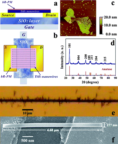 | ||
| Fig. 1 Structure of the TiO2 nanowires FET device. (a) Side view and (b) top view of the schematic structure; (c) AFM image of bR-PM (image size of 3.0 × 3.0 μm); (d) XRD spectrum of the TiO2 nanowires, lower part shows the standard diffraction peaks of anatase TiO2 (JCPDS No. 89-4921); (e) TiO2 nanowires alignment across the channel of electrodes under microscope (top view) and (f) SEM image of single TiO2 nanowire aligned across the channel. | ||
The effect of bR-PM modification on the output (ID–VD) and the transfer (ID–VG) characteristics of the TiO2 nanowires FET are shown in Fig. 2. Clearly, the modification of bR-PM on the TiO2 nanowires raises the drain current in n-channel operation (VG, VD < 0, Fig. 2a) whereas it reduces the drain current in p-channel operation (VG, VD > 0, Fig. 2b). The transfer characteristics demonstrate the same trend in Fig. 2c and 2d. The on/off ratio rises from approximately 9 to 12 for the TiO2 nanowires FET after bR-PM modification by changing the gate voltage from 0 to −25 V. Both output and transfer characteristics show clearly that bR-PM modification has the bidirectional mediation effect on the TiO2 nanowire FETs under different directions of the gate electric field. It is noteworthy that bR-PM modification can enhance the transfer and output characteristics of the FET when the applied gate voltage is negative.
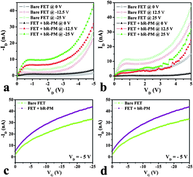 | ||
| Fig. 2 Effect of bR-PM on the TiO2 nanowires FET in the output (ID–VD) characteristics within (a) the negative gate voltage region and (b) the positive gate voltage region; and in the transfer (ID–VG) characteristics within the (c) negative gate voltage region and the (d) positive gate voltage region. | ||
Device mobility (μ) in the linear regime under negative gate bias was extracted following the equation (neglecting contact resistance) used by Cai et al.25 From our experimental results in Fig. 3, with imposed negative bias, the mobility of the bare TiO2 nanowires FET is 5.14 × 10⁻⁴ cm2 V−1 s−1 (corresponding to a carrier concentration of 5.67 × 10⁹ C cm−3), while after bR-PM modification, it increases by a factor of 2 to 9.93 × 10⁻⁴ cm2 V−1 s−1 (corresponding to a carrier concentration of 9.08 × 10⁹ C cm−3), indicating that the bR-PM modification can greatly enhance the hole mobility in TiO2 nanowires FET, which is consistent with the transfer and output characterization results (Fig. 2).
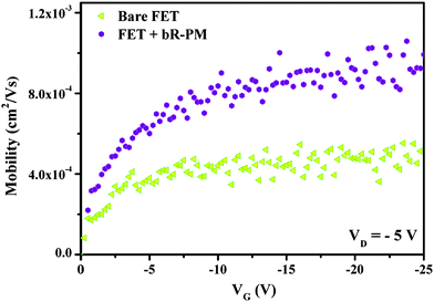 | ||
| Fig. 3 Mobility of the TiO2 nanowires FET before and after bR-PM modification. | ||
It is noticed that TiO2 is a material well known for its sensitivity to humidity.26 The modification of bR-PM from aqueous suspension could introduce moisture onto the TiO2 FET structure, causing high leakage current for an increased drain current. To exclude this possible reason, the humidity effect on the bR-PM modified FET was investigated. The ID–VD curves of the FETs were measured at a series of RH (Fig. 4), showing an increased drain current with RH increase for both FETs with and without the bR-PM modification. However, the increase caused by RH for both FETs with and without the bR-modification has almost the same magnitude, but is insignificant in comparison to the enhanced drain current by the bR-PM modification. In addition, since the ID–VD measurements of the FETs are conducted under low RH (<30%), the effect of humidity on the drain current of the bR-modified FET can be ignored.
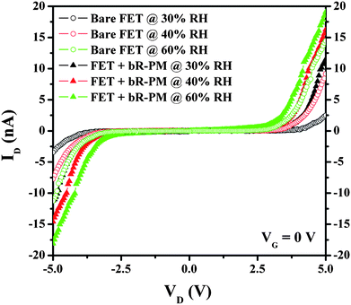 | ||
| Fig. 4 Effects of the RH change on TiO2 nanowires FET without and with bR-PM modification. | ||
The electric field induced by the permanent dipole of bR-PM is very likely to contribute to the enhanced performance of the bR-modified TiO2 nanowires FET under negative gate voltage. The EPS method employed in the bR-PM modification actually assured a preferred orientation of the membrane to generate EbR with a unidirection on the FET surface from the inherent dipoles of bR molecules. In terms of this presumption, the intensity of EbR can be theoretically estimated. The value of the dipole has been reported to be around 3.3 × 10⁻²⁸ C m per bR monomer,19 and it is known that bR-PM patches have a constant thickness of 5 nm.27 The formula for dipole moment calculation is
| P = q*d | (1) |
 | (2) |
As for the electric field generated by the gate voltage, which is termed as EG here, it can be calculated by formula
| EG = VG/d | (3) |
The influence of the layer number of bR-PM modified on the FET was investigated in order to confirm if the enhancement in the performance of the FET under negative gate voltage corresponds to the dipole's effect. For multilayer-oriented bR-PM modified on the TiO2 nanowires FET, although the layer number is increased, EbR of the deposited multilayer bR-PM will reduce as neutralization occurs between charges with different polarity on adjacent surfaces of the oriented membrane layers, and thus this results in a diminishing trend in the augmentation of the ID. By varying the concentration of the bR-PM suspension, bR-PM with different layer numbers can be deposited on the TiO2 nanowires FET to adjust the intensity of the electric field generated from the dipoles in the bR. Fig. 5 shows the relationship between the normalized ΔID (normalized ΔID = (ID (with bR-PM) − ID (without bR-PM))/ID (without bR-PM)) vs. the gate voltage after modification by bR-PM of different layer numbers. A reduction in ΔIDvs. the gate voltage can be observed as the layer number of bR-PM deposited on the TiO2 nanowires FET expands.
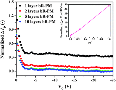 | ||
| Fig. 5 Effects of the deposited bR-PM of different layer number on the normalized ΔID of the TiO2 nanowires FET at VD = −5 V. Inset depicts the relationship between the percentage of the ΔID at the maximum gate voltage and the reciprocal of the square of the number of bR-PM layers modified. | ||
From our previous study,28 one patch layer of bR-PM is known to approximately correspond to an optical density expressed as OD560 = 0.0256. Thus, the layer number of bR-PM deposited on the FET device can be directly monitored by the OD560 of the multilayer membrane modified. A relationship between the concentrations of the bR-PM suspension and the optical density of the deposited multilayer membrane can also be established. With a bR-PM suspension of 2 mg ml−1 and a deposited amount of 1 μl, an OD560 = 0.256 of the resulted bR-PM membrane can be obtained, indicating that around 10 layers of PM patches can be deposited on the FET surface. Therefore, the layer number of bR-PM can be adjusted by applying a series of dilution factors in the 2 mg ml−1 bR-PM suspension. The relationship between the change of normalized ΔID, expressed as a percentage at the maximum gate voltage (in this case −25 V), and the reciprocal of the square of the modified bR-PM layer number is shown in the inset of Fig. 5. Theoretically, with the dilution factor of 1, 2, 5 and 10 applied in the 2 mg ml−1 bR-PM suspension, the corresponding layer numbers of bR-PM deposited on the FET are 10, 5, 2 and 1, respectively. If defining the electric field generated by the dipole moment from the bR-PM monolayer as EbR, the electric field generated by the dipole moment from 2, 5 and 10 layered bR-PM are 1/4 EbR, 1/25 EbR and 1/100 EbR, respectively. The quantitative trend obtained from the inset of Fig. 5 is very similar to the trend in the change of the theoretically calculated EbR, indicating that the drain current change is roughly in inverse proportion to the layer number of the deposited bR-PM, which is again well in agreement with our conclusion that the TiO2 nanowires FET can be influenced by dipole moment from the modified bR-PM.
The unidirectional permanent dipole existing within bR molecules is proposed here to account for the observed performance mediation of the TiO2 nanowires FET, as schematically shown in Fig. 6. With negative bias (Fig. 6a), EbR produced by the permanent dipole of bR is in the same direction as EG, the electric field produced by the gate voltage, and thus the bR-PM modification can increase the whole electric field applied to the TiO2 nanowires FET to generate a significantly larger drain current. When a positive gate voltage is applied (Fig. 6b), however, EbR is in the opposite direction to EG, thus bR-PM modification can weaken the whole electric field applied on the TiO2 nanowires FET and thus, the drain current is decreased. This approach may have universal significance to enhance the performance of other nanowire-based FETs.
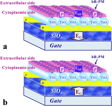 | ||
| Fig. 6 Schematic drawing of the relationship between the EbR and EG when (a) negative gate voltage and (b) positive gate voltage is applied to the TiO2 nanowires FET. | ||
Experimental
TiO2 nanowire preparation
The synthesis of TiO2 nanowires was completed by a hydrothermal synthesis method29 under a high pressure and high temperature environment, following the protocol reported by Chu et al.30 with minor modification. The TiO2 nanowire suspension at different concentrations was prepared in absolute ethanol by 5 min ultrasonication for optimization of concentration in the electric field-assisted alignment process.Purple membrane preparation
Bacteriorhodopsin-embedded purple membrane (bR-PM) was isolated from Halobacterial halobium S9 strain. Growth, purification, and sample preparation of the bR-PM were carried out according to the standard protocol31 with certain improved procedures. The absorption ratio of A280 nm/A570 nm was below 1.7, indicating that the bR-PM product was in good quality. In this study, the bR-PM fragments with a concentration of about 2 mg mL−1 bR at neutral pH were resuspended in Milli-Q H2O for about 120 s of ultrasonication.Patterning
Heavily n-doped silicon (Si) wafers with a 100 nm thick top oxide layer (SiO2) were patterned using photoresist AZ7220 (Clariant).25 After patterning, the wafers were introduced to an electron beam evaporator (BOC Edwards A306), and thin metal films (1 nm of Ti and 50 nm of Au) were deposited on them under a 1 × 10⁻⁶ Torr vacuum. After the deposition, the patterned photoresist was lifted off from the wafers by immersion in acetone assisted by gentle sonication to finalize the electrode patterning.Device fabrication
The silicon wafer and its surface SiO2 layer (100 nm), with a unit area capacitance of 34 nF cm−2,32 was employed as the gate electrode and gate dielectric, respectively. For all devices, the channel length and width were 2 and 1800 μm, respectively. The electrode-patterned wafers were briefly cleaned by sonication in acetone before use. With the Agilent 4284 LCR meter, the alignment of TiO2 nanowires across the electrode pair was conducted, which is based on dielectrophoretic forces in an alternating electric field to make the nanowires align parallel to the direction of the electric field. To contact both ends of most nanowires across the electrode pair, the alignment parameters were optimized before further experiments.After characterization and measurement of the TiO2 nanowires FET, electrophoretic sedimentation (EPS) was employed with a minor modification16c on the method of Wang et al.33 to immobilize the bR-PM onto the FET for mediation of its performance.
Characterization
Atomic force microscopy (AFM) studies were conducted to obtain the surface morphology of the bR-PM with a commercial Nanoman AFM (Dimension 3100 SPM, Veeco Metrology Group, USA) at ambient temperature in the contact mode using a commercial silicon tip (RTESP, Veeco, USA). The 3 × 3 μm image was recorded with a scan rate of 0.5 Hz in ambient air. The alignment of the TiO2 nanowire onto the as-prepared devices was examined by field-effect scanning electron microscopy (FESEM) (JEOL JSM-6700F FESEM). The powder X-ray diffraction (XRD) analysis was carried out with a Bruker D8- Advance X-Ray Diffractometer.The output as well as transfer characteristics of devices with and without bR-PM were characterized using an Agilent 4157B semiconductor parameter analyzer system under controlled relative humidity and nitrogen atmosphere, unless stated otherwise.
Conclusion
In this study, bR-PM-modified bottom-contact TiO2 nanowires FETs are fabricated and the dipole bio-originated from bR-PM is employed to tune the FET performance. It is demonstrated that with negative gate voltage, both transfer and output characteristics of the TiO2 nanowires FETs are improved with the hole mobility increased by a factor of 2 after bR-PM modification. By varying the concentration of the bR-PM suspension used in the modification, the layer number of bR-PM deposited onto the FET surface is found to affect the normalized ΔID, proving that it is the electric field generated by the dipole moment from the bR-PM that actually enhances the hole transport in the TiO2 nanowires FET. The bidirectional mediation of bR-PM on the performance of the FET provides a novel platform for the bioelectronics application of bR-PM.Acknowledgements
This work was financially supported by Center for Advanced Bionanosystems, Nanyang Technological University, Singapore.References
- (a) J. T. Hu, L. S. Li, W. D. Yang, L. Manna, L. W. Wang and A. P. Alivisatos, Science, 2001, 292, 2060–2063 CrossRef CAS; (b) X. G. Peng, L. Manna, W. D. Yang, J. Wickham, E. Scher, A. Kadavanich and A. P. Alivisatos, Nature, 2000, 404, 59–61 CrossRef CAS.
- (a) M. Kazes, D. Y. Lewis, Y. Ebenstein, T. Mokari and U. Banin, Adv. Mater., 2002, 14, 317–321 CrossRef CAS; (b) T.-S. Pui, A. Agarwal, F. Ye, Z.-Q. Tou, Y. Huang and P. Chen, Nanoscale, 2009, 1, 159–163 RSC.
- M. Law, L. E. Greene, J. C. Johnson, R. Saykally and P. D. Yang, Nat. Mater., 2005, 4, 455–459 CrossRef CAS.
- E. Stern, J. F. Klemic, D. A. Routenberg, P. N. Wyrembak, D. B. Turner-Evans, A. D. Hamilton, D. A. LaVan, T. M. Fahmy and M. A. Reed, Nature, 2007, 445, 519–522 CrossRef CAS.
- M. H. Huang, S. Mao, H. Feick, H. Q. Yan, Y. Y. Wu, H. Kind, E. Weber, R. Russo and P. D. Yang, Science, 2001, 292, 1897–1899 CrossRef CAS.
- S. J. Bao, C. M. Li, J. F. Zang, X. Q. Cui, Y. Qiao and J. Guo, Adv. Funct. Mater., 2008, 18, 591–599 CrossRef CAS.
- X. Chen and S. S. Mao, Chem. Rev., 2007, 107, 2891–2959 CrossRef CAS.
- S. J. Bao, Q. L. Bao, C. M. Li and Z. L. Dong, Electrochem. Commun., 2007, 9, 1233–1238 CrossRef CAS.
- Y. Qiao, C. M. Li, S. J. Bao, Z. S. Lu and Y. H. Hong, Chem. Commun., 2008, 1290–1292 RSC.
- Y. Qiao, S. J. Bao, C. M. Li, X. Q. Cui, Z. S. Lu and J. Guo, ACS Nano, 2008, 2, 113–119 CrossRef CAS.
- J. M. Baik, M. H. Kim, C. Larson, X. H. Chen, S. J. Guo, A. M. Wodtke and M. Moskovits, Appl. Phys. Lett., 2008, 92, 242111 CrossRef.
- Y. H. Lee, J. M. Yoo, D. H. Park, D. H. Kim and B. K. Ju, Appl. Phys. Lett., 2005, 86, 033110 CrossRef.
- D. Oesterhelt and W. Stoeckenius, Nat. New Biol., 1971, 233, 149–152 Search PubMed.
- U. Haupts, J. Tittor and D. Oesterhelt, Annu. Rev. Biophys. Biomol. Struct., 1999, 28, 367–399 CrossRef CAS.
- D. Oesterhelt and W. Stoeckenius, Proc. Natl. Acad. Sci. U. S. A., 1973, 70, 2853–2857 CAS.
- (a) K. Bradley, A. Davis, J. C. P. Gabriel and G. Gruner, Nano Lett., 2005, 5, 841–845 CrossRef CAS; (b) R. Li, F. Hu, Q. Bao, S. Bao, Y. Qiao, S. Yu, J. Guo and C. M. Li, Chem. Commun., 2010, 46, 689–691 RSC; (c) R. Li, C. M. Li, H. F. Bao, Q. L. Bao and V. S. Lee, Appl. Phys. Lett., 2007, 91, 223901 CrossRef; (d) T. Miyasaka, K. Koyama and I. Itoh, Science, 1992, 255, 342–344 CrossRef CAS.
- Y. Kimura, M. Fujiwara and A. Ikegami, Biophys. J., 1984, 45, 615–625 CAS.
- (a) R. A. Bogomolni, S. B. Hwang, Y. W. Tseng, G. I. King and W. Stoeckenius, Biophys. J., 1977, 17, A98–A98; (b) D. Xu, C. Martin and K. Schulten, Biophys. J., 1996, 70, 453–460 CAS.
- I. Ermolina, A. Lewis and Y. Feldman, J. Phys. Chem. B, 2003, 107, 14537–14544 CrossRef CAS.
- G. Wang and D. Porschke, J. Phys. Chem. B, 2003, 107, 4632–4638 CrossRef CAS.
- S. Suzuki, T. Yamanashi, S. Tazawa, O. Kurosawa and M. Washizu, IEEE Trans. Ind. Appl., 1998, 34, 75–83 CrossRef CAS.
- P. A. Smith, C. D. Nordquist, T. N. Jackson, T. S. Mayer, B. R. Martin, J. Mbindyo and T. E. Mallouk, Appl. Phys. Lett., 2000, 77, 1399–1401 CrossRef CAS.
- (a) R. Krupke, F. Hennrich, H. von Lohneysen and M. M. Kappes, Science, 2003, 301, 344–347 CrossRef CAS; (b) R. Krupke, F. Hennrich, H. B. Weber, D. Beckmann, O. Hampe, S. Malik, M. M. Kappes and H. V. Lohneysen, Appl. Phys. A: Mater. Sci. Process., 2003, 76, 397–400 CrossRef CAS.
- (a) A. Bezryadin, C. Dekker and G. Schmid, Appl. Phys. Lett., 1997, 71, 1273–1275 CrossRef CAS; (b) O. Harnack, C. Pacholski, H. Weller, A. Yasuda and J. M. Wessels, Nano Lett., 2003, 3, 1097–1101 CrossRef CAS.
- Q. J. Cai, M. B. Chan-Park, Z. S. Lu, C. M. Li and B. S. Ong, Langmuir, 2008, 24, 11889–11894 CrossRef CAS.
- (a) H. M. Liu, W. S. Yang, Y. Ma, Y. Cao, J. N. Yao, J. Zhang and T. D. Hu, Langmuir, 2003, 19, 3001–3005 CrossRef CAS; (b) J. S. Park and W. Choi, Langmuir, 2004, 20, 11523–11527 CrossRef CAS.
- N. Hampp, Chem. Rev., 2000, 100, 1755–1776 CrossRef CAS.
- R. Li, X. Cui, W. Hu, Z. Lu and C. M. Li, J. Colloid Interface Sci., 2010, 344, 150–157 CrossRef CAS.
- J. S. Chen, C. M. Li, W. W. Zhou, Q. Y. Yan, L. A. Archer and X. W. Lou, Nanoscale, 2009, 1, 280–285 RSC.
- Y. M. Chu, C. C. Lin, J. J. Wu, H. C. Chang, in 3rd IEEE International Conference of Nano/Micro Engineered and Molecular Systems, Sanya, PEOPLES R CHINA, 2008, pp 539–542 Search PubMed.
- D. Oesterhelt, W. Stoeckenius, in Methods Enzymol.Academic Press, San Diego, CA, 1974, vol. 31, pp 667–678 Search PubMed.
- Y. Gan, Q. J. Cai, C. M. Li, H. Bin Yang, Z. S. Lu, C. Gong and M. B. Chan-Park, ACS Appl. Mater. Interfaces, 2009, 1, 2230–2236 Search PubMed.
- J. P. Wang, S. K. Yoo, L. Song and M. A. ElSayed, J. Phys. Chem. B, 1997, 101, 3420–3423 CrossRef CAS.
| This journal is © The Royal Society of Chemistry 2010 |