Synthesis of nanometre-thick MoO3 sheets
Kourosh
Kalantar-zadeh
*ab,
Jianshi
Tang
c,
Minsheng
Wang
c,
Kang L.
Wang
c,
Alexandros
Shailos
d,
Kosmas
Galatsis
d,
Robert
Kojima
e,
Veronica
Strong
e,
Andrew
Lech
e,
Wojtek
Wlodarski
b and
Richard B.
Kaner
de
aDepartment of Chemistry, MIT, Cambridge, MA, USA. E-mail: kourosh@mit.edu
bSchool of Electrical and Computer Engineering, RMIT University, Melbourne, Australia. E-mail: kourosh.kalantar@rmit.edu.au
cElectrical Engineering Department, UCLA, Los Angeles, CA, USA. E-mail: wang@ee.ucla.edu
dCalifornia NanoSystems Institute (CNSI), UCLA, Los Angeles, USA. E-mail: shailos@cnsi.ucla.edu
eDepartment of Chemistry and Biochemistry, UCLA, Los Angeles, USA. E-mail: kaner@chem.ucla.edu
First published on 8th December 2009
Abstract
The formation of MoO3 sheets of nanoscale thickness is described. They are made from several fundamental sheets of orthorhombic α-MoO3, which can be processed in large quantities via a low cost synthesis route that combines thermal evaporation and mechanical exfoliation. These fundamental sheets consist of double-layers of linked distorted MoO6 octahedra. Atomic force microscopy (AFM) measurements show that the minimum resolvable thickness of these sheets is 1.4 nm which is equivalent to the thickness of two double-layers within one unit cell of the α-MoO3 crystal.
1. Introduction
Obtaining atomically thin layers by mechanical exfoliation has already triggered a plethora of research on graphene1,2 and certainly, the simplicity of this technique has made it attractive to many researchers. It is possible to extend the exfoliation method to layered structure materials other than graphene: many metal oxides such as MoO3, WO3 and V2O5 have stratified structures when they take special crystal phases.MoO3 is of special interest because of its multifaceted structural and functional properties. It is attractive for its photochromic3 and thermochromic4 properties and it is a widely used electrochromic material.5–8 It has also been shown that, as a functional material, MoO3 can be applied for generating enhanced electric field emission,9,10 in batteries,11 as a catalyst,12 and in gas sensors.13–18 Depending on the process, MoO3 can be synthesized in many different nano- or micro-structural morphologies that include wires, rods, belts, particles, and tubes.11,19–29 A number of different techniques have been reported for the deposition of MoO3, including pulsed laser deposition,30 thermal evaporation,10,31–34 sputtering,15,35,36 sol–gel,13,16,17 hydrothermal,37 spray pyrolysis,38 chemical vapour deposition,5,39 and electrodeposition.8,40 The deposition of MoO3 using evaporative techniques is particularly advantageous as it can produce highly crystalline and stratified structures. These are important features for our work since both high crystallinity and layer formation are the necessary conditions for mechanical exfoliation in order to obtain sheets of nano thickness. In addition, the thermal evaporation of MoO3 is also high yield, low cost, and can produce large crystals made of nano thin sheets with significant dimensions. The possibility of forming MoO3 layers of less than 10 nm thickness has been suggested by Kim and Leiber.41 However, such a layer was specifically formed on MoS2 surface by thermal oxidation, which limits its application for device fabrication. Our work provides a facile process for forming such layers on any substrate.
The structural determination of MoO3 is necessary to predict and identify the mechanism of how it behaves during deposition and mechanical exfoliation. The structural chemistry of the molybdenum oxides, was first described several decades ago in a series of seminal manuscripts by Kihlborg.42 Two of the most common crystal phases of MoO3 are known as α-MoO3 and metastable β-MoO3.43,44 These two phases have very different physical and chemical properties including refractive indices, bandgap energies, and mechanical hardness. In the temperature range 370–400 °C a spontaneous transformation of β → α phase takes place.45 Orthorhombic α-MoO3 is of special interest for this research as it possesses a unique two-dimensional layered structure suitable for mechanical exfoliation.
MoO3 has the space group Pbnm with unit cell parameters a = 13.86 Å, b = 3.70 Å and c = 3.96 Å (JCPD file: 05-0508). α-MoO3 is lamellar46 and insoluble in water.47 Its stratified structure facilitates the injection of different donor ions into the free spaces, and thus creating its favourable electrochromic and gasochromic properties. α-MoO3 consists of double-layers of linked distorted MoO6 octahedra (Fig. 1). In each double-layer, MoO6 octahedra form edge-sharing zig-zag rows along the [001] direction and corner sharing rows along the [100] direction. The adjacent layers along [010] are linked only by weak van der Waals forces to make the lamellar formation,48,49 while the internal interactions between atoms within the double-layers are dominated by strong ionic and covalent bonding.50 The nature of the Mo–O bond changes considerably with the equilibrium bond distance, and varies from strongly covalent for the shortest bond to predominantly ionic for the longest bonds in the MoO6 octahedron.51–53 The fundamental thickness of a double-layer including one van der Waals gap is 1.386 nm. The [100], [010] and [001] projected structures of α-MoO3 are shown in Fig. 1.
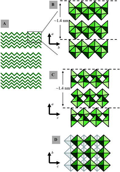 | ||
| Fig. 1 Selected representations of α-MoO3: (A) the formation of secondary crystallite networks (B, C and D) of edge- and corner-sharing MoO6 octahedra viewed along different crystallographic planes. | ||
Having made the stratified structure and knowing that the layers are bonded together by weak van der Waal’s forces, we chose α-MoO3 with the assumption that thin layers of the order of unit cell dimensions can be formed after mechanical exfoliation.
2. Experimental and results
Evaporation was employed for the formation of stratified crystallites of orthorhombic α-MoO3 by subliming the source material in powder form, and subsequently depositing the vapour onto a substrate at a predetermined temperature region. In our process, 10 mg of the MoO3 powder (China Rare Metal Material Co.) was weighed and placed at the centre of a horizontal furnace. The substrates were placed at a certain distance from the central hot spot at a temperature of approximately 400 °C and thermal deposition was carried out using a carrier gas (argon). Deposition took place for 1 h and the evaporation temperature was increased slowly at the rate of 5 °C per min and cooled at the same rate after the procedure.MoO3 was deposited onto several different substrates including Si and SiO2 (Fig. 2). When α-MoO3 was grown at the temperature of 400 °C there was no special preferential growth, resulting in random crystallite orientations. The dimensions of the crystallites depended on the flow rate and temperature, with thinner and smaller crystallites achieved at higher flow rates and substrate temperatures. At high flow rates, nanobelts are formed and growth in the [001] direction becomes prominent. As can be seen in Fig. 2, the crystallites are made of nanometre-thick sheets (which in this work, we call “secondary clusters”) stacked on top of each other. These secondary fundamental sheet clusters are the building blocks of larger tertiary crystallites.
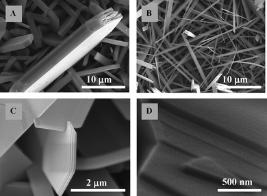 | ||
| Fig. 2 SEM images of MoO3 deposited on Si and SiO2 at (A) low gas flow rate and (B) high gas flow rate (C, D) at different scales. | ||
The thickness of the secondary sheets can be obtained from powder X-ray diffraction (PXRD) peak broadening using the Scherrer equation. These secondary layers were calculated to have an average thickness of 25 nm using our deposition conditions. Changing the deposition conditions such as the flow rate and temperature alters their thickness. For instance, Siciliano, et al.32 reported 85 nm for their MoO3, while Hsu, et al.7 found that the cluster thickness changed from 10 to 25 nm when their annealing temperature was increased from 200 to 500 °C. The thickness of these secondary clusters affects the exfoliation. We observed that after the first few initial steps of mechanical exfoliation, predominantly nanosheets of 25 nm were formed before continuing the process and eventually reaching thicknesses of several atomic layers.
The XRD pattern, transmission electron microscopy (TEM) image and selected area electron diffraction (SAED) pattern of some large crystallites are shown in Fig. 3. The strongest diffraction peaks for MoO3 in the XRD pattern appear at 12.8°, 25.7°, 39.0° 2θ, which correspond to the (020), (040) and (060) planes, respectively, and are attributed to planes normal to the [010] direction. The SAED diffraction pattern shows growth along [001] and [100] for the orthorhombic MoO3 sheets, which is in agreement with a literature report.29 This emphasizes the presence of α-MoO3 comprised of parallel sheets of MoO3 double-layers which is suitable for mechanical exfoliation.
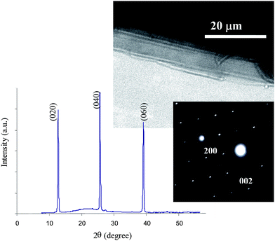 | ||
| Fig. 3 XRD pattern, TEM image and SAED pattern of the secondary crystals. | ||
Mechanical exfoliation was conducted similar to the exfoliation of graphene.1,2,54 First, the MoO3 crystallites were mechanically separated from the substrate and subsequently were placed on Scotch tape (3M), which resulted in millimetre- to micrometre-sized MoO3 fragments. The mechanical exfoliation using Scotch tape was repeated 15 to 20 times until only a faint reflection of a MoO3 layer could be observed. We then placed the tape on a SiO2 (300 nm)/Si substrate and peeled it off. The SiO2/Si had been plasma treated beforehand to increase the adhesion of MoO3 sheets and to obtain thinner layers. Without plasma treatment the thicknesses were generally greater than 25 nm. However, plasma treatment of the substrates resulted in a large number of sheets with thicknesses less than 14 nm being anchored to the substrates.
High-resolution TEM (HRTEM) and atomic force microscopy (AFM) were utilized to assess the MoO3 sheets. HRTEM images were taken using a Titan G2 FEI. As can be seen in Fig. 4, two sets of parallel fringes appeared with a spacing of 0.39 and 0.36 nm, which correspond to the (100) and (001) planes, respectively. Combined with the information in Fig. 3, these results suggest that the nanosheets grow strongly along both [100] and [001] directions which are normal to the [010] direction.22,23 The exposure time to the electron beam must be kept at a minimum to obtain the correct lattice fringes, as long exposures gradually transform MoO3 to MoO2 and eventually to MoO.55,56
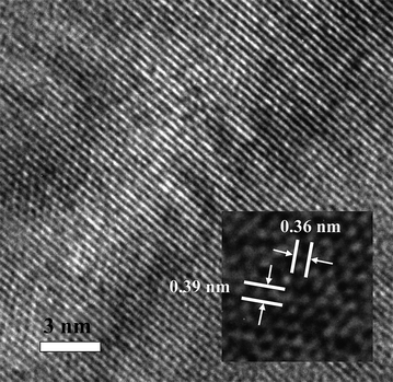 | ||
| Fig. 4 HRTEM image of nanometre-thin MoO3 sheets. | ||
Atomic force microscopy (AFM) was carried out using a Nanoscope V Dimension Icon (Veeco Instruments) under ambient conditions. A large number of MoO3 crystallites with 4 to 20 double-layers were resolved (with thicknesses of 2.8 to 14 nm) along with many other secondary clusters ranging from 20 to 65 nm in thickness. An initial optical observation was used in order to distinguish between layers of different thicknesses. As can be seen in Fig. 5, thinner layers appeared green in colour and thicker layers were yellow, orange and red – this series of colours was repeated as the layer became thicker and thicker.
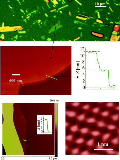 | ||
| Fig. 5 Typical optical (above) and corresponding AFM images and profiles of MoO3 sheets. | ||
It seems that the mechanical exfoliation effectively separates layers at their weakest bonds, where they are held together by weak van der Waals forces. No individual double-layer was found that existed independently; however, many four double-layer thick sheets appeared as an extended bottom layer in many profile measurements. These sheets all had a fundamental thickness of 2.8 nm (essentially twice the magnitude of a = 1.389 nm) which is in agreement with the thickness of four double-layers plus their four corresponding van der Waals gaps. According to the α-MoO3 crystal structure (Fig. 1), the double-layers are repeated in the ab-plane along the a-axis; while the repeat in the ac-plane along the a-axis occurs for every two consecutive double-layers. As a result, it is possible that the crystal only favors breaks at the boundary of these two double-layer repeat units while requiring the existence of at least one non-repeat unit. The other thicknesses also followed this quantized step of 1.4 nm and were all multiples of the fundamental number of the unit cell parameters a = 13.86 Å. On average the observed steps were 2.8, 4.2, …, and 14 nm which correspond to an even number of double-layers: 4, 5, …, 20 double-layers of α-MoO3. High-resolution contact AFM also provides evidence for the existence of a repeat unit with dimensions of approximately 0.4 × 0.4 nm and contours with the height of 0.65 nm which is a strong confirmation of the α-MoO3.43
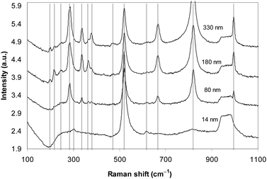
Raman spectroscopy was employed to further confirm that the stratified material is made of double-layers of MoO3. MoO3 of four different thicknesses of 14, 80, 180 and 330 nm were targeted to investigate the thinning effect by exfoliation on Raman spectra.32,57,58 As can be seen in Fig. 6, the Si substrate signature always appears as a strong peak at 520 cm−1 and a broad flat band that covers the area from 930 to 1000 cm−1. For all MoO3 of 80, 180 and 330 nm thickness strong typical 284, 671, 999 and 821 cm−1 peaks were observed. The 284 cm−1 peak represents the wagging mode for the double bond O![[double bond, length as m-dash]](https://www.rsc.org/images/entities/char_e001.gif) MoO. The 671 cm−1 peak is assigned to the triply coordinated oxygen (Mo3–O) stretching mode which results from edge-shared oxygen atoms in common to three octahedral. The 821 cm−1 peak is for the doubly coordinated oxygen (Mo2–O) stretching mode which results from corner-sharing oxygen atoms common to two octahedra. Finally, the peak at 999 cm−1 is assigned to the terminal oxygen (Mo6+O) stretching mode which results from an unshared oxygen.
MoO. The 671 cm−1 peak is assigned to the triply coordinated oxygen (Mo3–O) stretching mode which results from edge-shared oxygen atoms in common to three octahedral. The 821 cm−1 peak is for the doubly coordinated oxygen (Mo2–O) stretching mode which results from corner-sharing oxygen atoms common to two octahedra. Finally, the peak at 999 cm−1 is assigned to the terminal oxygen (Mo6+O) stretching mode which results from an unshared oxygen.
 | ||
| Fig. 6 The Raman spectra of MoO3 samples of different thicknesses. | ||
The 336, 378, and 365 cm−1 peaks are assigned to O–Mo–O bending and scissoring modes,32 which become constantly weaker by thinning. Interestingly, for the 180 nm- and 330 nm-thick samples the stronger 198 cm−1 peak and two other weaker peaks at 217 and 246 cm−1 are observed which represent the OMoO twist, the AgRc chain mode and B3g, OMoO twist modes, respectively. They, however, have much lower intensity than reported by others and also gradually disappear as the layered sheet becomes thinner, and vanish in the 80 nm-thick sample spectra. The commonly observed strong 115 and 159 cm−1 peaks32,36 were not seen by us. Possibly the adhesion to the SiO2/Si surface reduces peak intensities in the region below 250 cm−1.
For the thin layer of thickness 14 nm, the strongest peaks include the 671 cm−1 peak which represents the triply coordinated oxygen stretching and the 821 cm−1 peak which is for the doubly coordinated oxygen (Mo2–O) stretching mode. They assert the existence of the double-layer in the thinnest sheets formed on the surface. Additionally, two extra peaks are also observed: a peak at 615 cm−1 starts appearing for thicknesses of less than 100 nm and becomes relatively strong in the spectrum of the 14 nm-thick samples. This peak has not previously been reported for MoO3 but peaks at similar locations have been reported for the hydrated form.59 The other peak that appears at 299 cm−1 might result from the slight shift of the initially strong 284 cm−1 peak, representing the wagging mode for the double bond OMoO, either due to adhesion onto the substrate or the hydration. The measurements that were conducted using fresh samples after annealing (300 °C) also showed these peaks. Layers are thin and can readily adsorb water, so we suggest that the further annealing and Raman measurements should be conducted in a vacuum environment to draw an accurate conclusion.
Conclusions
In conclusion, we have demonstrated the synthesis of nanometre-thin – almost two-dimensional (2D) – metal oxides made of double-layered fundamental α-MoO3 sheets that can be prepared by mechanical exfoliation of thermally evaporated crystals. This class of 2D crystal offers a wide range of possibilities for the development of novel optical and electronic devices. After the emergence of 1D metal oxide materials such as ZnO nanorods and belts, and 2D graphene, a plethora of devices were developed. Similar investigations on the present class of metal oxides could be applied with the difference that the quantum properties will be affected by its 2D structure.Acknowledgements
The authors thank the Department of Innovation, Industry, Research and Science, Australia (ISL grant # CG130115) for financially supporting this linkage international project.References
- K. S. Novoselov, A. K. Geim, S. V. Morozov, D. Jiang, Y. Zhang, S. V. Dubonos, I. V. Grigorieva and A. A. Firsov, Science, 2004, 306, 666–669 CrossRef CAS.
- K. S. Novoselov, D. Jiang, F. Schedin, T. J. Booth, V. V. Khotkevich, S. V. Morozov and A. K. Geim, Proc. Natl. Acad. Sci. U. S. A., 2005, 102, 10451–10453 CrossRef CAS.
- J. N. Yao, K. Hashimoto and A. Fujishima, Nature, 1992, 355, 624–626 CrossRef CAS.
- M. A. Quevedo-Lopez, R. F. Reidy, R. A. Orozco-Teran, O. Mendoza-Gonzalez and R. Ramirez-Bon, J. Mater. Sci.: Mater. Electron., 2000, 11, 151–155 CrossRef CAS.
- K. Gesheva, A. Szekeres and T. Ivanova, Sol. Energy Mater. Sol. Cells, 2003, 76, 563–576 CrossRef.
- N. A. Chernova, M. Roppolo, A. C. Dillon and M. S. Whittingham, J. Mater. Chem., 2009, 19, 2526–2552 RSC.
- C. S. Hsu, C. C. Chan, H. T. Huang, C. H. Peng and W. C. Hsu, Thin Solid Films, 2008, 516, 4839–4844 CrossRef.
- A. Guerfi, R. W. Paynter and L. H. Dao, J. Electrochem. Soc., 1995, 142, 3457–3464 CAS.
- Y. B. Li, Y. Bando, D. Golberg and K. Kurashima, Appl. Phys. Lett., 2002, 81, 5048–5050 CrossRef CAS.
- J. Zhou, N. S. Xu, S. Z. Deng, J. Chen, J. C. She and Z. L. Wang, Adv. Mater., 2003, 15, 1835–1840 CrossRef CAS.
- S. H. Lee, Y. H. Kim, R. Deshpande, P. A. Parilla, E. Whitney, D. T. Gillaspie, K. M. Jones, A. H. Mahan, S. B. Zhang and A. C. Dillon, Adv. Mater., 2008, 20, 3627 CrossRef CAS.
- A. Bielanski and M. Najbar, Appl. Catal., A, 1997, 157, 223–261 CrossRef CAS.
- A. K. Prasad, D. J. Kubinski and P. I. Gouma, Sens. Actuators, B, 2003, 93, 25–30 CrossRef.
- J. Okumu, F. Koerfer, C. Salinga and M. Wuttig, J. Appl. Phys., 2004, 95, 7632–7636 CrossRef CAS.
- M. Ferroni, V. Guidi, G. Martinelli, P. Nelli, M. Sacerdoti and G. Sberveglieri, Thin Solid Films, 1997, 307, 148–151 CrossRef CAS.
- K. Galatsis, Y. X. Li, W. Wlodarski, E. Comini, G. Sberveglieri, C. Cantalini, S. Santucci and M. Passacantando, Sens. Actuators, B, 2002, 83, 276–280 CrossRef.
- K. Galatsis, Y. X. Li, W. Wlodarski and K. Kalantar-zadeh, Sens. Actuators, B, 2001, 77, 478–483 CrossRef.
- A. M. Taurino, A. Forleo, L. Francioso, P. Siciliano, M. Stalder and R. Nesper, Appl. Phys. Lett., 2006, 88, 152111 CrossRef.
- G. T. Chandrappa and J. Livage, 2006.
- S. Phadungdhitidhada, P. Mangkorntong, S. Choopun and N. Mangkorntong, Ceram. Int., 2008, 34, 1121–1125 CrossRef CAS.
- E. Comini, L. Yubao, Y. Brando and G. Sberveglieri, Chem. Phys. Lett., 2005, 407, 368–371 CrossRef CAS.
- Q. P. Ding, H. B. Huang, J. H. Duan, J. F. Gong, S. G. Yang, X. N. Zhao and Y. W. Du, J. Cryst. Growth, 2006, 294, 304–308 CrossRef CAS.
- L. Fang, Y. Y. Shu, A. Q. Wang and T. Zhang, J. Phys. Chem. C, 2007, 111, 2401–2408 CrossRef CAS.
- S. Hu and X. Wang, J. Am. Chem. Soc., 2008, 130, 8126 CrossRef CAS.
- X. W. Lou and H. C. Zeng, Chem. Mater., 2002, 14, 4781–4789 CrossRef CAS.
- X. W. Lou and H. C. Zeng, J. Am. Chem. Soc., 2003, 125, 2697–2704 CrossRef CAS.
- M. Niederberger, F. Krumeich, H. J. Muhr, M. Muller and R. Nesper, J. Mater. Chem., 2001, 11, 1941–1945 RSC.
- G. R. Patzke, A. Michailovski, F. Krumeich, R. Nesper, J. D. Grunwaldt and A. Baiker, Chem. Mater., 2004, 16, 1126–1134 CrossRef CAS.
- T. A. Xia, Q. Li, X. D. Liu, J. A. Meng and X. Q. Cao, J. Phys. Chem. B, 2006, 110, 2006–2012 CrossRef CAS.
- V. Bhosle, A. Tiwari and J. Narayan, J. Appl. Phys., 2005, 97, 083539 CrossRef.
- D. Dhawan, S. Bhargava, J. Tardio, W. Wlodarski and K. Kalantar-Zadeh, 2008, 6, pp. 231–236.
- T. Siciliano, A. Tepore, E. Filippo, G. Micocci and M. Tepore, Mater. Chem. Phys., 2009, 114, 687–691 CrossRef CAS.
- J. Yu, S. J. Ippolito, M. Shafiei, D. Dhawan, W. Wlodarski and K. Kalantar-zadeh, Appl. Phys. Lett., 2009, 94, 013504 CrossRef.
- J. Zhou, S. Z. Deng, N. S. Xu, J. Chen and J. C. She, Appl. Phys. Lett., 2003, 83, 2653–2655 CrossRef CAS.
- A. K. Prasad, P. I. Gouma, D. J. Kubinski, J. H. Visser, R. E. Soltis and P. J. Schmitz, Thin Solid Films, 2003, 436, 46–51 CrossRef CAS.
- I. Navas, R. Vinodkumar, K. J. Lethy, A. P. Detty, V. Ganesan, V. Sathe and V. P. M. Pillai, J. Phys. D: Appl. Phys., 2009, 42, 175305 CrossRef.
- S. T. Wang, Y. G. Zhang, X. C. Ma, W. Z. Wang, X. B. Li, Z. D. Zhang and Y. T. Qian, Solid State Commun., 2005, 136, 283–287 CrossRef CAS.
- A. Bouzidi, N. Benramdane, H. Tabet-Derranz, C. Mathieu, B. Khelifa and R. Desfeux, Mater. Sci. Eng., B, 2003, 97, 5–8 CrossRef.
- Y. J. Lee, W. T. Nichols, D. G. Kim and Y. Do Kim, J. Phys. D: Appl. Phys, 2009, 42, 5.
- R. S. Patil, M. D. Uplane and P. S. Patil, Appl. Surf. Sci., 2006, 252, 8050–8056 CrossRef CAS.
- Y. Kim and C. M. Lieber, Science, 1992, 257, 375–377 CAS.
- L. Kihlborg, Arkiv for Kemi, 1963, 21, 357 Search PubMed.
- R. L. Smith and G. S. Rohrer, J. Solid State Chem., 1996, 124, 104–115 CrossRef CAS.
- P. F. Carcia and E. M. McCarron, Thin Solid Films, 1987, 155, 53–63 CrossRef CAS.
- W. M. R. Divigalpitiya, R. F. Frindt and S. R. Morrison, Thin Solid Films, 1990, 188, 173–179 CrossRef CAS.
- L. Kihlborg, Advances in Chemistry Series, American Chemical Society, Washington, 1963, 39 Search PubMed.
- W. T. Elwell and D. F. Wood, Pergamon Press, New York, 1971.
- S. S. Sunu, E. Prabhu, V. Jayaraman, K. I. Gnanasekar, T. K. Seshagiri and T. Gnanasekaran, Sens. Actuators, B, 2004, 101, 161–174.
- D. Dhawan, S. Bhargava, J. Tardio, W. Wlodarski and K. Kalantar-Zadeh, Sens. Lett., 2008, 6, 231–236 CrossRef CAS.
- B. Gerand and L. Seguin, Solid State Ionics, 1996, 84, 199–204 CrossRef CAS.
- R. Radhakrishnan, C. Reed, S. T. Oyama, M. Seman, J. N. Kondo, K. Domen, Y. Ohminami and K. Asakura, J. Phys. Chem. B, 2001, 105, 8519–8530 CrossRef CAS.
- F. Corà, A. Patel, N. M. Harrison, C. Roetti and C. R. A. Catlow, J. Mater. Chem., 1997, 7, 959–967 RSC.
- T. Learmonth, C. McGuinness, P. A. Glans, B. Kennedy, J. S. John, J. H. Guo, M. Greenblatt and K. E. Smith, Phys. Rev. B: Condens. Matter Mater. Phys., 2009, 79, 035110 CrossRef.
- M. Bruna and S. Borini, J. Phys. D: Appl. Phys., 2009, 42, 175307 CrossRef.
- D. Wang, D. S. Su and R. Schlogl, Z. Anorg. Allg. Chem., 2004, 630, 1007–1014 CrossRef CAS.
- R. Coquet and D. J. Willock, Phys. Chem. Chem. Phys., 2005, 7, 3819–3828 RSC.
- S. H. Lee, M. J. Seong, C. E. Tracy, A. Mascarenhas, J. R. Pitts and S. K. Deb, Solid State Ionics, 2002, 147, 129–133 CrossRef CAS.
- K. Eda, J. Solid State Chem., 1992, 98, 350–357 CrossRef CAS.
- L. Seguin, M. Figlarz, I. R. Cavagnat and J.-C. Lasskgues, Spectrochim. Acta, Part A, 1995, 51, 1323–1344 CrossRef.
| This journal is © The Royal Society of Chemistry 2010 |