Wall-to-wall stress induced in (6,5) semiconducting nanotubes by encapsulation in metallic outer tubes of different diameters: A resonance Raman study of individual C60-derived double-wall carbon nanotubes
Federico
Villalpando-Paez
*a,
Hiroyuki
Muramatsu
b,
Yoong Ahm
Kim
c,
Hootan
Farhat
d,
Morinobu
Endo
e,
Mauricio
Terrones
f and
Mildred S.
Dresselhaus
g
aDepartment of Materials Science and Engineering, Massachusetts Institute of Technology, Cambridge, MA 02139-4307, USA
bInstitute of Carbon Science and Technology, Shinshu University, 4-17-1 Wakasato, Nagano-shi 380-8553, Japan
cFaculty of Engineering, Shinshu University 4-17-1 Wakasato, Nagano-shi 380-8553, Japan. AND Institute of Carbon Science and Technology, Shinshu University, 4-17-1 Wakasato, Nagano-shi 380-8553, Japan
dDepartment of Materials Science and Engineering, Massachusetts Institute of Technology, Cambridge, MA 02139-4307, USA
eFaculty of Engineering, Shinshu University 4-17-1 Wakasato, Nagano-shi 380-8553, Japan. AND Institute of Carbon Science and Technology, Shinshu University, 4-17-1 Wakasato, Nagano-shi 380-8553, Japan
fLaboratory for Nanoscience and Nanotechnology Research (LINAN) AND Advanced Materials Department, IPICYT, San Luis Potosí 78216, México
gDepartment of Physics AND Department of Electrical Engineering and Computer Science, Massachusetts Institute of Technology, Cambridge, MA 02139-4307, USA
First published on 24th November 2009
Abstract
We measure resonant Raman scattering from 11 individual C60-derived double-wall carbon nanotubes all having inner semiconducting (6,5) tubes and various outer metallic tubes. The Raman spectra show the radial breathing modes (RBM) of the inner and the outer tubes to be simultaneously in resonance with the same laser energy. We observe that an increase in the RBM frequency of the inner tubes is related to an increase in the RBM frequency of the outer tubes. The Raman spectra also contain a sharp G− feature that increases in frequency as the nominal diameter of the outer metallic tubes decreases. Finally, the one-phonon second-order D-band mode shows a two-way frequency splitting that decreases with decreasing nominal wall-to-wall distance. We suggest that the stress which increases with decreasing nominal wall-to-wall distance is responsible for the hardening that is observed in the frequencies of the RBM, D and G− modes of the inner (6,5) semiconducting tubes.
1. Introduction
Double-wall carbon nanotubes (DWNTs) exhibit optical and vibrational properties that are similar to those of single-wall carbon nanotubes (SWNTs) but their double-wall structure makes them more mechanically and thermally robust.1 Depending on the metallic (M) or semiconducting (S) nature of their inner and outer tubes, DWNTs can have four possible configurations, S@S, S@M, M@S, M@M, each of which is expected to have particular properties suitable for different electronic device applications.Possible techniques for fabricating DWNTs include chemical vapor deposition (CVD)1,2 or the filling of SWNTs with fullerenes that coalesce and form inner tubes of DWNTs upon heat treatment.3,4 Both types of DWNTs are studied in the present work and are inter-compared. In the case of C60-derived DWNTs (denoted by C60-DWNTs), the coalescence of fullerenes at high temperature (>1200 °C) forms inner tubes with diameters (dt) close to that of C60.4 According to Bandow et al., under prolonged heat treatment the initial diameters of the inner tubes can increase in order to adjust the wall-to-wall (WtW) distances and minimize the energy of the system.4 Also, by using high-resolution Raman spectroscopy, Pfeiffer et al.5–8 and Kuzmany et al.,9 observed that the inner tubes of C60-DWNTs can be contained inside outer tubes with different diameters where smaller WtW distances increase the inter-tube interaction and upshift the radial breathing mode (RBM) of the inner tubes. CVD-DWNTs and C60-DWNTs have been shown to have different optical properties that are believed to originate from differences in the WtW distances and the degree of crystallinity of the inner tubes. For instance, on one hand, a quenching of the photoluminescence (PL) signal has been observed in C60-DWNTs and attributed to inter-tube interactions.10 On the other hand, in CVD-DWNTs, a strong PL emission from the inner semiconducting tubes has been recently reported.11
To the best of our knowledge, most spectroscopic experiments on DWNTs have been performed on bundles or solution-based samples, so that it has been inherently difficult to use Raman spectroscopy to investigate which inner (n,m) tubes are actually contained inside the variety of observed outer (n′,m′) tubes. In order to quantitatively determine which specific inner and outer tubes actually form each DWNT, one must perform experiments on individual DWNTs.12 Therefore, in the present work individual C60-DWNTs have been dispersed on a substrate and studied independently. Here we report a brief comparison between CVD-DWNT and C60-DWNT bundles and a detailed study of 11 individual isolated C60-DWNTs with inner semiconducting (6,5) tubes and various outer metallic tubes.
2. Experimental details
We used a CVD method to synthesize the CVD-DWNT bundles used in this study. The high purity of our CVD-DWNT bundles relative to residual catalyst particles and SWNTs has been confirmed by diamagnetic susceptibility13,14 and Raman spectroscopy experiments,15 respectively. The C60-DWNT bundles used herein were fabricated by reacting C60 and SWNTs under vacuum at 600 °C for 24 h. The starting SWNT material was synthesized by the arc-discharge method and purified by Hanwha Corp (Korea). The as-grown peapods were washed with toluene to remove residual C60 and heat treated at 1700 °C in Ar (1 atm) to transform them into C60-DWNT bundles. A high-resolution transmission electron microscopy (HRTEM) image of the resulting C60-DWNT material is shown in Fig. 1(a). A solution containing isolated C60-DWNTs was prepared by dispersing 1 mg of C60-DWNTs in D2O with 0.5 wt% sodium dodecylbenzene sulfonate (SDBS) and sonicating the dispersion (600 W cm−2) for 15–30 min. Subsequently, the solution was ultracentrifuged (320![[hair space]](https://www.rsc.org/images/entities/char_200a.gif) 000 g) for 30 min and 70% of the supernatant solution was collected. Photoluminescence measurements were performed on the resulting C60-DWNT solution with a NIR-PL Shimazu system using a liquid-nitrogen-cooled InGaAs array-type detector. The PL map from the C60-DWNT solution (see Fig. 1(b)) shows the presence of three (n,m) species where the strongest peak corresponds to (6,5) semiconducting tubes.
000 g) for 30 min and 70% of the supernatant solution was collected. Photoluminescence measurements were performed on the resulting C60-DWNT solution with a NIR-PL Shimazu system using a liquid-nitrogen-cooled InGaAs array-type detector. The PL map from the C60-DWNT solution (see Fig. 1(b)) shows the presence of three (n,m) species where the strongest peak corresponds to (6,5) semiconducting tubes.
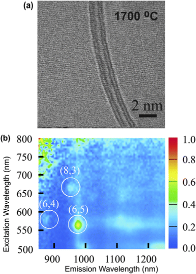 | ||
| Fig. 1 (a) HRTEM image of a C60-DWNT produced by heat treating peapods at 1700 °C in Ar (b) Photoluminescence (PL) map of a solution containing isolated C60-DWNTs dispersed in sodium dodecylbenzene sulfonate (SDBS). The strongest PL peak corresponds to semiconducting (6,5) inner tubes. | ||
The solution containing isolated C60-DWNTs was spin-coated on a silicon substrate that is marked with a gold grid and allows for precise recording of the location of an isolated DWNT [see inset of Fig. 2(b)].12 The distribution of the deposited DWNTs on the silicon substrate is not spatially homogeneous but the nanotube density is low enough to have 0 to 20 nanotubes per 100 μm2. The laser spot has a 1 μm diameter and, depending on its location on the substrate, the laser spot illuminated 0 to 5 DWNTs. For bundles, five measurements were performed on different spots and laser power levels were kept below 0.5 mW to avoid excessive heating of the DWNTs. The scattered light was collected through a 100× objective using a backscattering geometry. An Nd:YAG laser was used to generate Elaser = 2.33 eV and a Kr+ ion laser generated Elaser = 1.92 eV. A dye laser containing Rhodamine 6Gdye and a Ti:sapphire laser were pumped by the Nd:YAG laser to generate Elaser = 2.05–2.16 eV and Elaser = 1.6 eV, respectively. A thermoelectrically-cooled Si CCD (charge coupled device) detector operating at −75 °C was used to collect Raman spectra.
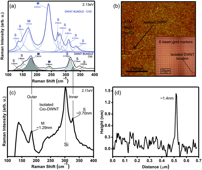 | ||
| Fig. 2 (a) Raman spectra for the RBM region for CVD-DWNT and C60-DWNT bundles (Elaser = 2.13 eV). (b) Atomic force microscope (AFM) image of one individual, isolated DWNT. Inset: Silicon substrate with Au markers showing the location of the DWNT. (c) Raman spectra for the RBM Raman region (Elaser = 2.11 eV) for an isolated individual C60-DWNT and (d) AFM height profile of the individual, isolated DWNT shown in (b) with the RBM spectrum shown in (c). The vertical lines connecting (a) and (c) show that the ωRBM of the prominent tube diameters observed in the C60-DWNT bundles coincide with the ωRBM of the inner and outer tubes of the isolated C60-DWNTs. | ||
In order to obtain a strong Raman signal from an isolated carbon nanotube, the resonance condition must be met by matching the laser energy to the energy separation between the van Hove singularities of the isolated nanotube.16 Our laser spot often illuminates nanotubes that are not in resonance with the laser energy. Therefore, in order to find resonant nanotubes with a strong radial breathing mode (RBM) Raman signal, we scanned large substrate areas (900 μm2).
3. Results and discussion
3.1 Bundle DWNTs
Before starting the discussion on individual C60-DWNTs, we briefly comment on the RBM spectra of our C60-DWNT and CVD-DWNT bundle samples. As shown in Fig. 2(a), and in agreement with a previous report,8C60-DWNTs have a narrower dt distribution than CVD-DWNTs. This observation was expected because, in the case of C60-DWNTs, the dt distribution of the starting SWNT material limits the possible choice of dt for the inner tubes when the fullerenes coalesce through heat treatment. In the case of CVD-DWNTs, this dt limitation is not present and, when using Elaser = 2.13 eV, we find resonance with semiconducting tubes for 8 different diameters and metallic tubes with dt = 1.41 and 0.97 nm [see Fig. 2(a)]. As is expected, the RBM frequencies of the inner and outer tubes of the individual C60-DWNTs that we study in the following section, coincide with the RBM frequencies of the most prominent tube diameters observed in the C60-DWNT bundles [See vertical lines connecting the shaded Lorentzians in Fig. 2(a) to the RBM pair in Fig. 2(c)].3.2 Isolated, individual C60-DWNTs
Herein we describe the procedures that allowed us to detect isolated C60-DWNTs and we then discuss the dependence of the ωRBM, ωG− and ωD frequencies on DWNT nominal inner tube diameter and WtW distance.After studying the large area Raman maps of the Si substrate, on a few occasions (ca. <5%), it was possible to find locations on the Si substrate that showed two RBM modes, simultaneously in resonance with the same Elaser. These pairs of RBMs come from two nanotubes, one with a small diameter (∼0.7 nm) and another one with a large (∼1.3 nm) diameter. The observation of these RBM pairs [see Fig. 2(c)] suggested that we had found a resonance with the inner and outer tubes of the same DWNT. However, although the probability is low, a rope of 2–3 DWNTs could also generate a pair of RBMs if the inner and outer tubes of two different DWNTs happen to be in resonance with the same Elaser. Therefore, in order to confirm that the two observed RBMs were indeed coming from the same DWNT, we verified that only one DWNT was being illuminated by the laser spot. This verification consisted of three steps whose results are shown, for the same DWNT, in Fig. 2:
(1) We used AFM (atomic force microscopy) to check that the DWNT was completely isolated and far away from the other tubes on the substrate [see Fig. 2(b)]. The inset in Fig. 2(b) shows the Au grid used to mark and record the location of each individual DWNT.
(2) We checked that the height of the DWNT as measured by AFM corresponds to the diameter of the outer tube of the DWNT as deduced from its low-frequency RBM. Fig. 2(d) shows the AFM height profile of our DWNT. The difference between the measured Raman and AFM outer tube diameter estimates is ∼0.1 nm.
(3) Finally we scan the same spot in the sample with multiple laser lines in order to eliminate the presence of additional nanotubes that might not have been in resonance with the initial laser energy. Fig. 2(c) shows the RBM region of the Raman spectrum coming from one isolated DWNT taken with Elaser = 2.11 eV. The same spot on the substrate was also scanned with nine different laser energies (2.33, 2.16, 2.14, 2.12, 2.10, 2.07, 2.05, 1.92 and 1.60 eV) and no additional RBMs coming from other nanotubes were detected.
Performing AFM and acquiring Raman spectra with many Elaser on isolated DWNTs is feasible12 but also experimentally challenging. While attempting to increase the throughput of the above mentioned technique, we discovered that it is also possible to use less AFM time and only one laser line and still be almost certain that we are in resonance with the inner and outer tubes of the same DWNT. We now describe a new procedure that allowed us to detect 11 isolated C60-DWNTs.
First we used one laser line (2.08 or 2.10 eV) to find as many spectra as possible containing two simultaneous RBMs (see Fig. 3) that matched the expected inner and outer tube diameters of the individual DWNTs present in our sample (see Fig. 4). By plotting the low-frequency RBM (large diameter outer tubes) vs. high-frequency RBM (small diameter inner tubes) for each spectrum, we found that the frequencies of most of the simultaneously detected RBM pairs (80%) were correlated [see Fig. 5(a)]. We know a priori that if the two simultaneously resonant RBMs do not correspond to the same DWNTs we should observe random low-frequency RBM vs. high-frequency RBM relationships. Therefore, the trend followed by the simultaneous RBM pairs plotted in Fig. 5(a) suggests that each RBM pair is indeed coming from the inner and outer tubes of a single isolated DWNT. Thus, if the observed pair of RBMs fits the trend in Fig. 5(a), then the pair is identified as most likely coming from the same isolated DWNT and the pair is then retained; otherwise the spectra are discarded in this analysis.
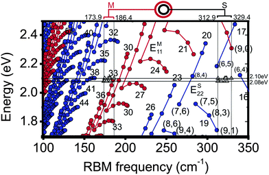 | ||
| Fig. 3 Kataura plot of the resonant transition energies vs. RBM frequencies for SWNTs based on the extended tight binding model.17 The location on the plot of the measured DWNT RBMs are marked with triangles. The laser energies (2.08 and 2.10 eV) chosen to excite DWNTs with inner semiconducting and outer metallic tubes are marked with horizontal lines. The vertical lines denote the ranges of ωRBM measured for the inner and outer tubes. | ||
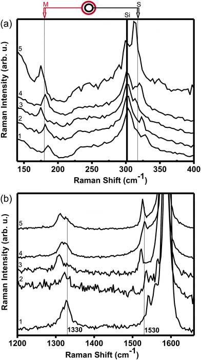 | ||
| Fig. 4 (a) RBM-band and (b) D and G-band regions of the Raman spectra corresponding to five different DWNTs whose inner and outer walls are simultaneously in resonance with the same laser line Elaser = 2.10 eV. Vertical lines in (a) denote outer M tubes and inner S (6,5) tubes and the dark vertical line denotes a Si Raman feature. The vertical lines in (b) denote D- and G-band features (see text). | ||
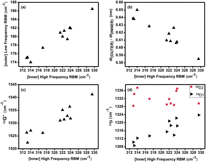 | ||
| Fig. 5 All the inner tubes for the 11 C60-DWNTs in this figure are (6,5) tubes. (a) Correlation between the ωRBM of the inner and outer tubes of the same C60-DWNT. (b) Correlation between the WtW distance of each DWNT with ωRBM for its inner tube. An increase in the ωRBM of the inner tubes is accompanied by a decrease in the nominal WtW distance. (c) Plot of ωG−vs. ωRBM for the inner tube of each DWNT. An upshift in ωG− results from a decrease in the nominal WtW distance and the resulting increased inter-tube interaction. (d) The ωD1 for each component of the D-band vs. ωRBM for the inner tube for each of the 11 DWNTs. The splitting of the D-band into ωD1 and ωD2 decreases as ωRBM of the inner tube increases with decreasing nominal WtW distance. Note that ωD2 remains almost constant while ωD1 increases. | ||
The Kataura plot in Fig. 3 shows that, when using Elaser = 2.08 and 2.10 eV, we excited the ES22 transitions of (6,5) inner semiconducting tubes and the EM11 transitions of outer metallic tubes mainly from family 2n + m = 33. The Kataura plot was calculated within the ETB (extended tight binding) framework,17 including many-body corrections, fitted to the RRS (resonance Raman scattering) data from sodium dodecyl sulfate-wrapped HiPCO (high-pressure CO conversion) SWNTs.18 We find that such a Kataura plot (Fig. 3) which is based on prior studies on SWNTs,17 is accurate enough for the qualitative identification of the (n,m) assignment for small diameter tubes within DWNTs. Although the relationship between ωRBM and dt for the inner tubes and outer tubes of DWNTs is not expected to be the same as it would be for isolated SWNTs, we approximate the nanotube diameters for both the inner and outer tubes of DWNTs in this work by using the SWNT-based RBM relation ωRBM = 218.3/dt + 15.9,14 because there are no experimental or theoretical ωRBMvs. dt relationships presently available for the inner and outer tubes that constitute the four different kinds of DWNT configurations (S@S, S@M, M@S, M@M) as mentioned above. Also, nanotube–substrate van der Waals interactions are known to induce radial deformations that can upshift the ωRBM of large-diameter SWNTs.19 However, in this work we assume that nanotube–substrate interactions have a negligible effect on the ωRBM of each of the two layers of our DWNTs because (a) the dt of the outer tubes is relatively small (1.3 nm) and therefore has a small contact area with the substrate, (b) the deformation of the outer tube is reduced by the presence of the inner tube, and (c) because, to a first order approximation, the inner tube is shielded and not affected by the substrate.
Based on the SWNT-based RBM relation mentioned above, we find that the ωRBM values for the 11 DWNT specimens experimentally measured in this work yield nominal inner (outer) tube diameters in the 0.69–0.73 nm (1.28–1.35 nm) range. The nominal WtW distances for these 11 C60-DWNTs are calculated by subtracting the nominal dt of the inner tubes from the nominal dt of the outer tubes obtained by the above procedure, yielding nominal WtW distances in the 0.58–0.65 nm range. In Fig. 5(a) we plot the measured ωRBM of each inner tube vs. the ωRBM of its corresponding outer tube for the 11 measured tubes. All the inner tubes in this work are assigned to (6,5) nanotubes and we observe that their measured ωRBM values upshift with increasing measured outer tube ωRBM values [Fig. 5(a)]. Similarly, the measured ωRBM of the inner tubes upshifts with decreasing nominal WtW distance as shown in Fig. 5(b) and in qualitative agreement with the results in refs. 5–9.
Because of the strong carbon–carbon bond and the small dt of the (6,5) tubes, we do not expect the actual diameter of the inner tubes to decrease to the values given by the SWNT-based ωRBMvs. 1/dt relation given above. Instead, the observed hardening of the measured ωRBM as the nominal WtW distance decreases corresponds to a minimal change in actual inner tube dt and provides an indirect measure of the stress that is felt by the inner tube. All of the 11 inner tubes shown herein are Type II semiconducting (6,5) tubes but the outer tubes that surround them vary somewhat in diameter and can be identified with a few different (n,m) values from one another, but certainly far less than 11 different values.
Since the inner tubes of our DWNTs are semiconducting, their spectra show sharp G− features that are easy to fit unambiguously with a Lorentzian lineshape. If we correlate ωG−, the frequency of the G−-band, to the low frequency RBM (corresponding to the inner tube) in our spectra for DWNTs, we observe an increase in ωG− as ωRBM for the inner nanotube increases [see Fig. 5(c)]. This behavior is opposite to the well-documented diameter dependence of the G− (LO) mode in S-SWNTs.16
We explain this observation in the following way. We know from Fig. 5(b) that DWNTs whose inner tube show an upshifted ωRBM tend to have smaller nominal WtW distances. A smaller nominal WtW distance implies a higher degree of inter-tube interaction and a higher mutually induced stress felt by both the inner and outer tubes of an individual DWNT. Therefore, we expect the observed hardening of the G− frequency with increasing inner tube ωRBM [see Fig. 5(c)] to be caused by the increased stress that the outer and inner tubes exert on each other in the case of DWNTs as the WtW distances decrease. Experimentally, although not shown explicitly in this work, the intensity of the G−-band is not observed to show any significant dependence on the nominal WtW distance.
Finally, we expect the G+ region of our DWNTs to contain a contribution from the LO mode of its S inner tube and the TO mode of its M outer tube. Unfortunately, the ωG+ of the inner tubes and the ωG+ of the outer tubes from our DWNTs overlap so that we can not distinguish the separate contributions made by each of the tubes to the G+ feature and we were not able to study possible correlations between ωG+ and the ωRBM of the inner nanotube.
4. Conclusions
In this work we obtained the Raman spectra of 11 isolated C60-DWNTs all with inner semiconducting (6,5) tubes but with different outer metallic tubes by searching for RBM pairs that were simultaneously in resonance with the same Elaser and that matched the expected inner and outer tube diameters of individual DWNTs. In this collection of isolated C60-DWNTs we observed that the ωRBM of the inner (6,5) semiconducting tube hardens as the diameter of the outer metallic tube decreases. We also measured an increase in ωG− with decreasing wall-to-wall distances and attributed the upshift of ωG− to the stress felt by the inner tubes of the DWNTs due to increasing inter-tube interaction and mutual stress. Finally, we noted that the D-band mode splits into two components where the lower frequency component ωD1 is related to the inner tube and hardens with decreasing nominal WtW distances. The upper frequency D-band component ωD2 related to the outer tube is independent of the nominal WtW distance. In the future we expect to use the same technique to find specimens with the remaining three DWNT configurations and compare their optical properties as the inter-tube distances are varied.Acknowledgments
The authors gratefully acknowledge financial support from CONACYT Mexico: 56787 (Laboratory for Nanoscience and Nanotechnology Research-LINAN), 45772 (M.T.), 58899-Inter American Collaboration (M.T.), the MIT-CONACYT program (M.S.D., M.T.), 2004-01-013/SALUD-CONACYT(M.T.). We also thank CONACYT graduate student grants, Vilore Foods Co. and SEP Mexico for financial support (F.V.P). The authors M.E., Y.A.K and H.M. acknowledge support from the CLUSTER project (second stage) and a grant for Specially Promoted Research (No. 19002007) from the Ministry of Education, Culture, Sports, Science and Technology of Japan. The authors F.V.P., and M.S.D. gratefully acknowledge support from NSF/DMR 07–04197. The authors are grateful to D. Nezich for providing marked Si substrates and to A. Reina, M. Hofmann, E. Barros, A. G. Souza and L. G. Cancado for helpful discussions.References
- Y. A. Kim, H. Muramatsu, T. Hayashi, M. Endo, M. Terrones and M. S. Dresselhaus, Chem. Phys. Lett., 2004, 398, 87–92 CrossRef CAS.
- M. Endo, H. Muramatsu, T. Hayashi, Y. A. Kim, M. Terrones and N. S. Dresselhaus, Nature, 2005, 433, 476–476 CrossRef CAS.
- S. Bandow, M. Takizawa, H. Kato, T. Okazaki, H. Shinohara and S. Iijima, Chem. Phys. Lett., 2001, 347, 23–28 CrossRef CAS.
- S. Bandow, T. Hiraoka, T. Yumura, K. Hirahara, H. Shinohara and S. Iijima, Chem. Phys. Lett., 2004, 384, 320–325 CrossRef CAS.
- R. Pfeiffer, C. Kramberger, F. Simon, H. Kuzmany, V. N. Popov and H. Kataura, Eur. Phys. J. B, 2004, 42, 345–350 CrossRef CAS.
- R. Pfeiffer, F. Simon, H. Kuzmany and V. N. Popov, Phys. Rev. B: Condens. Matter Mater. Phys., 2005, 72, 161404 CrossRef.
- R. Pfeiffer, F. Simon, H. Kuzmany, V. N. Popov, V. Zolyomi and J. Kurti, Phys. Status Solidi B, 2006, 243, 3268–3272 CrossRef CAS.
- R. Pfeiffer, H. Peterlik, H. Kuzmany, F. Simon, K. Pressi, P. Knoll, M. H. Rummeli, H. Shiozawa, H. Muramatsu, Y. A. Kim, T. Hayashi and M. Endo, Phys. Status Solidi B, 2008, 245, 1943–1946 CrossRef CAS.
- H. Kuzmany, W. Plank, R. Pfeiffer and F. Simon, J. Raman Spectrosc., 2008, 39, 134–140 CrossRef CAS.
- T. Okazaki, S. Bandow, G. Tamura, Y. Fujita, K. Iakoubovskii, S. Kazaoui, N. Minami, T. Saito, K. Suenaga and S. Iijima, Phys. Rev. B: Condens. Matter Mater. Phys., 2006, 74, 153404 CrossRef.
- D. Shimamoto, H. Muramatsu, T. Hayashi, Y. A. Kim, M. Endo, J. S. Park, R. Saito, M. Terrones and M. S. Dresselhaus, Appl. Phys. Lett., 2009, 94, 083106 CrossRef.
- F. Villalpando-Paez, H. Son, D. Nezich, Y. P. Hsieh, J. Kong, Y. A. Kim, D. Shimamoto, H. Muramatsu, T. Hayashi, M. Endo, M. Terrones and M. S. Dresselhaus, Nano Lett., 2008, 8, 3879–3886 CrossRef CAS.
- Y. A. Kim, H. Muramatsu, T. Hayashi, M. Endo, M. Terrones and M. S. Dresselhaus, Chem. Vap. Deposition, 2006, 12, 327 CrossRef CAS.
- M. Endo, Y. A. Kim, T. Hayashi, H. Muramatsu, M. Terrones, R. Saito, F. Villalpando-Paez, S. G. Chou and M. S. Dresselhaus, Small, 2006, 2, 1031–1036 CrossRef CAS.
- Y. Kim, H. Muramatsu, M. Kojima, T. Hayashi, M. Endo, M. Terrones and M. Dresselhaus, Chem. Phys. Lett., 2006, 420, 377–381 CrossRef CAS.
- M. Dresselhaus, G. Dresselhaus, R. Saito and A. Jorio, Phys. Rep., 2005, 409, 47–95 CrossRef.
- G. G. Samsonidze, R. Saito, N. Kobayashi, A. Gruneis, J. Jiang, A. Jorio, S. G. Chou, G. Dresselhaus and M. S. Dresselhaus, Appl. Phys. Lett., 2004, 85, 5703–5705 CrossRef CAS.
- A. Jorio, C. Fantini, M. Pimenta, R. B. Capaz, G. G. Samsonidze, M. S. Dresselhaus, N. Kobayashi, A. Gruneis and R. Saito, Phys. Rev. B: Condens. Matter Mater. Phys., 2005, 71, 075401 CrossRef.
- L. Gomez-De Arco, B. Lei, S. Cronin and C. W. Zhou, Appl. Phys. Lett., 2008, 93, 123112 CrossRef.
- R. Saito, A. Jorio, J. H. Hafner, C. M. Lieber, M. Hunter, T. McClure, G. Dresselhaus and M. S. Dresselhaus, Phys. Rev. B: Condens. Matter Mater. Phys., 2001, 64, 085312 CrossRef.
- S. Piscanec, M. Lazzeri, J. Robertson., A. C. Ferrari and F. Mauri, Phys. Rev. B: Condens. Matter Mater. Phys., 2007, 75, 035427 CrossRef.
- A. Jorio, A. G. Souza, G. Dresselhaus, M. S. Dresselhaus, A. K. Swan, M. S. Unlu, B. B. Goldberg, M. A. Pimenta, J. H. Hafner, C. M. Lieber and R. Saito, Phys. Rev. B: Condens. Matter Mater. Phys., 2002, 65, 155412–9 CrossRef.
| This journal is © The Royal Society of Chemistry 2010 |