Superconducting tantalum disulfide nanotapes; growth, structure and stoichiometry†
Charles W.
Dunnill
a,
Ian
MacLaren
b and
Duncan H.
Gregory
*a
aWestCHEM, Department of Chemistry, University of Glasgow, Joseph Black Building, Glasgow, G12 8QQ, UK. E-mail: D.Gregory@chem.gla.ac.uk
bDepartment of Physics & Astronomy, University of Glasgow, Kelvin Building, Glasgow, G12 8QQ, UK. E-mail: I.Maclaren@physics.gla.ac.uk
First published on 27th October 2009
Abstract
Superconducting tantalum disulfidenanowires have been synthesised by surface-assisted chemical vapour transport (SACVT) methods and their crystal structure, morphology and stoichiometry studied by powder X-ray diffraction (PXD), scanning electron microscopy/energy dispersive X-ray spectroscopy (SEM/EDX), transmission electron microscopy (TEM), selected area electron diffraction (SAED) and nanodiffraction. The evolution of morphology, stoichiometry and structure of materials grown by SACVT methods in the Ta–S system with reaction temperature was investigated systematically. High-aspect-ratio, superconducting disulfidenanowires are produced at intermediate reaction temperatures (650 °C). The superconducting wires are single crystalline, adopt the 2H polytypic structure (hexagonal space group P63/mmc: a = 3.32(2) Å, c = 12.159(2) Å; c/a = 3.66) and grow in the <2![[1 with combining macron]](https://www.rsc.org/images/entities/char_0031_0304.gif) 0> direction. The nanowires are of rectangular cross-section forming nanotapes composed of bundles of much smaller fibres that grow cooperatively. At lower reaction temperatures nanowires close to a composition of TaS3 are produced whereas elevated temperatures yield platelets of 1T TaS2.
0> direction. The nanowires are of rectangular cross-section forming nanotapes composed of bundles of much smaller fibres that grow cooperatively. At lower reaction temperatures nanowires close to a composition of TaS3 are produced whereas elevated temperatures yield platelets of 1T TaS2.
Introduction
Since the observation of anisotropic nanofibrous inorganic materials in 19791 significant interest has developed in the nanostructures of the group 4, 5 and 6 transition metal dichalcogenides. The group 6 disulfidenanotubes, MoS2 and WS2, were first characterised in 19922 following the discovery of carbon nanotubes by Iijima3 one year earlier. In the subsequent period, research into the scope of inorganic structures formed by these materials has now grown considerably with a plethora of different inorganicnanofibre, (tubes, rods, ribbons, belts, wires etc.) systems known.4,5 For example, the group 6 disulfides, WS2 and MoS2, form nanofibres with demonstrable potential as solid lubricants for applications where graphite is not suitable.2Tantalum disulfide, TaS2, like many other transition metal dichalcogenides, exists in a number of different polytypes resulting from the different possible stacking arrangements of the S–Ta–S sandwich layers (in which the metal is typically coordinated in either octahedral or trigonal prismatic geometry to sulfur). These have been much studied and were first described systematically by Jellinek in 1962.6 The most common polytypes are the 1T, 2H and 3R (single-layered trigonal, double-layered hexagonal and triple-layered rhombohedral respectively) structures (Fig. 1) although the 6-layer rhombohedral structure, denoted 6R, and 4-layer hexagonal (4H) structure have also been observed with some frequency. Both rhombohedral polymorphs have been described as metastable (kinetically stable at room temperature).7 The 2H structure thus contains layers of Ta–S trigonal prisms and in the bulk, the 2H form of TaS2 is metallic with a conduction band that is predominantly metal dz2 in character.8 2H TaS2 displays intriguing electronic properties in that it undergoes a transition to a charge density wave (CDW) state at 70 K and then a further transition to a superconducting state at 0.8 K.9 By contrast, the 1T polytype (containing Ta–S octahedra) is non-superconducting at ambient pressure and forms an incommensurate CDW state below 550 K.10 An important recent development, however, has been the inducement of superconductivity in 1T-TaS2 at high pressure; the first instance of superconductivity in any 1T-structured transition metal dichalcogenide.11
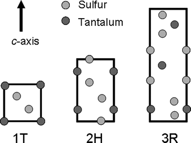 | ||
| Fig. 1 Schematic illustrating the stacking sequences and coordination in the 1T, 2H and 3R polytype of TaS2. The structures are shown as projections onto the (110) plane.6 | ||
In a previous communication we demonstrated that nanowires of tantalum disulfide could be synthesised in a single-step surface-assisted chemical vapor transport (SACVT) process .12 Importantly, the disulfidenanowires that we produced by SACVT were superconducting with an approximately 5-fold increase in transition temperature compared to that of bulk 2H-TaS2. The crystal- and precise micro-structure of the superconducting nanowires, however, remain to be determined and these issues have to be addressed if one is to understand the origin of the superconductivity in the nanostructured disulfides. Further, there is a need to understand how these nanowires form and grow and what influence this growth process and the resulting morphology has upon their electronic structure and physical properties.
Here we describe the evolution of morphology, stoichiometry and structure of materials grown by SACVT methods in the Ta–S system with reaction temperature. We demonstrate that high-aspect-ratio superconducting disulfidenanowires are produced at intermediate reaction temperatures (650 °C); below this temperature nanowires close to a composition of TaS3 are produced while at higher temperatures nanowire formation is curtailed and succeeded by formation of characteristic crystalline platelets (with the 1T structure). Importantly, a systematic study of the micro- and crystal structure of the superconducting nanostructures reveals first that the wires are of rectangular cross-section forming nanotapes composed of bundles of much smaller fibers and second that these superconducting disulfide nanotapes are of the 2H polytype.
Results and discussion
Products of varying morphology were observed under the different reaction temperatures, as shown in Fig. 2. Sample 1, prepared at a final dwell temperature of 400 °C, produced a black polycrystalline powder in region I of the ampoules (see experimental section and ref. 12), but yielded no nanofibrous material in region II (or region I), indicating that 400 °C was below the required temperature for the formation of nanowires. The black powder in region I was identified as a mixture of both the 2H and 3R polytypes of TaS2 plus the starting materials by the comparison of PXD data with patterns from structures on the ICDD PDF database.6,13,14 By contrast, sample 2 (500 °C) produced nanofibres that were ribbon-like in appearance and gave a PXD pattern unlike the other materials synthesised at lower or higher temperatures. EDX analysis indicated a higher sulfur content (Ta:S ratio of 1 : 3) and hence the likely presence of TaS3. The PXD pattern of 2 however was neither a good match to that calculated from the single-crystal structure of monoclinic TaS3,15 nor could it be indexed to the earlier reported orthorhombic form of the trisulfide (for which no refined crystal structure is known),6 possibly eluding to a new phase. TaS3 is known to be thermodynamically stable at lower temperatures and thermally decomposes at higher temperatures into TaS2.16 The stoichiometry and crystal structure of 2 is currently under further investigation. Product 3 took the form of high-aspect-ratio nanowires and as the main focus of this paper, is discussed in more detail below. Products 4 and 5 prepared with upper dwell temperatures of 750 °C and 900 °C respectively were formed as low yields of nanofibrous material, nucleating in small, isolated clusters on the foil substrate. These fibrous products were of a fine, feathered appearance and again yielded an EDX Ta:S ratio of 1 : 2. Reaction 6 showed no evidence of nanofibrous material in region II of the ampoules, and given also the low yields of fibrous material in 5, suggests that the thermal stability of these materials could lie close to 900 °C. The PXD patterns of the powders recovered from region I of these ampoules heated at 1100 °C (Fig. 3) show a good match to the 1T polytype of TaS2 which has been previously reported as the stable and prevalent high temperature phase at this composition in the Ta–S binary phase system.7SEM micrographs reveal products from 6, region I to be well defined platelets of the order of 10–50 µm across (Fig. 2d).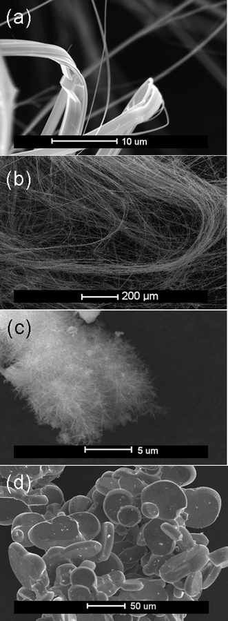 | ||
| Fig. 2 SEM micrographs of: (a) Nanoribbons (2) formed at 500 °C, (b) high-aspect-ratio nanowires (3) formed at 650 °C, (c) fine nanowires (5) formed at 900 °C and (d) platelets (6) formed at 1100 °C (recovered from region I of the ampoule). | ||
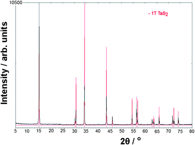 | ||
| Fig. 3 PXD pattern for the platelets (6) formed at 1100 °C showing a match to the pattern calculated from the structure of the 1T polytype of TaS2 (red). | ||
Fig. 2b shows typical fibres formed at 650 °C (3) under the conditions described in the experimental section. Unsurprisingly given their morphology, the nanowires exhibit extreme 00l preferred orientation, but PXD data (Fig. 4) demonstrate that 3 is TaS2. The patterns can be fit approximately to more than one of the possible polymorphs, but most convincingly to either the 2H or 3R structures. In fact, the best refined cell parameters were obtained when the PXD reflections were indexed to the 2H structure, yielding values of a = 3.32(2) Å and c = 12.159(2) Å; c/a = 3.66. This represents an expansion along c of ca. 0.5% compared to single crystals of (“bulk”) 2H-TaS2 (a = 3.314(1) Å, c = 12.097(1); c/a = 3.65).17
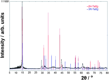 | ||
| Fig. 4 PXD pattern for 3 with comparisons to the calculated patterns generated from the 2H (red) and 3R (blue) polytype structures. | ||
Nath and Rao18 previously described the possible preference for nanotubes of TaS2 to form with the 2H structure on the basis of PXD patterns, however differentiation of the polytypes by PXD alone can be difficult and inconclusive given the similarities in the crystal structures and, for example, the tendency for the nanocrystallites to align and exhibit preferred orientation (along the [00l] direction). SEM images (Fig. 2b) confirmed the extremely anisotropic morphology of the samples prepared at 650 °C; 3 forms wires exhibiting exceptionally high aspect ratios (typically > 50![[hair space]](https://www.rsc.org/images/entities/char_200a.gif) 000 : 1), lengths in excess of 3 mm and widths of 50–500 nm. The stoichiometry from EDX was seen to be 36 : 64(2) (taken from spot scans across multiple regions of several samples). This equates, within error, to the expected 33.3 : 66.7 (1 : 2) Ta:S ratio for TaS2 but nevertheless raises the possibility of metal (or sulfur) non-stoichiometry (e.g. Ta1+xS2). One also needs to consider, however, the inherent errors of EDX performed on samples of non-uniform (surface) morphology. EDX results from samples from the other reactions yielded similar elemental ratios in all cases for nanofibrous products with the exception of 2 as described above. SQUID data for 3 show a superconducting transition at 3.4 K and as previously outlined (see the ESI† ).12 Of the bulk TaS2 phases, only the 2H and 6R polytypes are superconducting at ambient pressure (Tc = 0.8 K and 2.3 K respectively)9,19 which might suggest initially that the likelihood is that the nanowires adopt one of these two polytypic structures. Notably also, nanobelts with the 6R structure are reported to superconduct at 2.7 K,16 while bulk 6R TaS2 has a Tc > 4 K at 17.3 kbar19 and bulk 1T TaS2 (non-superconducting at ambient pressure) becomes superconducting with Tc = 6 K at 1 GPa and above, as discovered very recently.11
000 : 1), lengths in excess of 3 mm and widths of 50–500 nm. The stoichiometry from EDX was seen to be 36 : 64(2) (taken from spot scans across multiple regions of several samples). This equates, within error, to the expected 33.3 : 66.7 (1 : 2) Ta:S ratio for TaS2 but nevertheless raises the possibility of metal (or sulfur) non-stoichiometry (e.g. Ta1+xS2). One also needs to consider, however, the inherent errors of EDX performed on samples of non-uniform (surface) morphology. EDX results from samples from the other reactions yielded similar elemental ratios in all cases for nanofibrous products with the exception of 2 as described above. SQUID data for 3 show a superconducting transition at 3.4 K and as previously outlined (see the ESI† ).12 Of the bulk TaS2 phases, only the 2H and 6R polytypes are superconducting at ambient pressure (Tc = 0.8 K and 2.3 K respectively)9,19 which might suggest initially that the likelihood is that the nanowires adopt one of these two polytypic structures. Notably also, nanobelts with the 6R structure are reported to superconduct at 2.7 K,16 while bulk 6R TaS2 has a Tc > 4 K at 17.3 kbar19 and bulk 1T TaS2 (non-superconducting at ambient pressure) becomes superconducting with Tc = 6 K at 1 GPa and above, as discovered very recently.11
Fig. 5a shows a bright-field TEM image of a section of a typical TaS2nanowire from sample 3. A rather more atypical case is shown in Fig. 5b where a wire is twisted and shows a rather thin section at the centre where the lateral width of the wire is small, although the thickness in the beam direction is clearly fairly large, since this section is barely electron transparent. TEM investigations revealed that typical individual nanowires were of the order of 100–500 nm across. An SAED pattern from this nanowire in shown in Fig. 6a and may be indexed as a [0001] zone axis pattern, as is also shown in the simulation of Fig. 6b. Since the rotation between the image and the diffraction modes in the TEM is well known, it was straightforward to determine that the long axis of the crystal runs along one of the ⅓〈20〉 crystal directions. Unfortunately, the 1T, 2H, and 3R phases of TaS2 all produce almost identical diffraction patterns along [0001] and this pattern cannot be used to distinguish between the polytypes. The ideal solution would be to have the crystal oriented along a direction in the basal plane, since the periodicity in the c-direction could then be directly determined from the diffraction patterns, but this orientation could not be achieved in the samples mounted on carbon films, except possibly in some cases where the wire was too thick to remain electron transparent.
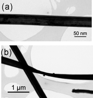 | ||
| Fig. 5 Bright-field TEM image of a section of TaS2nanowires (3): (a) Typical flat wire; (b) twisted wire. | ||
![Image and diffraction patterns of a TaS2nanowire (3): (a) SAED pattern at 0° tilt; (b) simulated [0001] diffraction pattern; (c) SAED pattern after a 10° tilt about the wire axis; (d) simulated 10° tilt pattern; (e) SAED pattern after a 20° tilt about the wire axis; (f) simulated 20° tilt pattern.](/image/article/2010/NR/b9nr00224c/b9nr00224c-f6.gif) | ||
| Fig. 6 Image and diffraction patterns of a TaS2nanowire (3): (a) SAED pattern at 0° tilt; (b) simulated [0001] diffraction pattern; (c) SAED pattern after a 10° tilt about the wire axis; (d) simulated 10° tilt pattern; (e) SAED pattern after a 20° tilt about the wire axis; (f) simulated 20° tilt pattern. | ||
For this reason, the nanowire was tilted about its long axis in 10° steps. After a 10° tilt, a pronounced spot splitting is observed in the direction perpendicular to the wire axis (arrowed in Fig. 6c). Comparisons with a diffraction pattern simulated for the 2H polytype tilted 10° about [20] (Fig. 6d) result in indices for these split spots of 02![[2 with combining macron]](https://www.rsc.org/images/entities/char_0032_0304.gif) 1 and 022 in one direction, and 02 and 02 in the other. If attempts are made to index these spots for the 1T or 3R polytypes, the only outcome is to obtain fractional indices, i.e. 02½/
1 and 022 in one direction, and 02 and 02 in the other. If attempts are made to index these spots for the 1T or 3R polytypes, the only outcome is to obtain fractional indices, i.e. 02½/ for 1T and as 02
![[/]](https://www.rsc.org/images/entities/char_e0ee.gif) /
/ for 3R. This clearly rules out any match to the 1T or 3R phases. The 6R phase would produce additional split reflections, which are not seen, and this possibility can therefore also be excluded.
After a 20° tilt a more pronounced spot splitting is observed between 011 and 012, as can be seen in Fig. 6e and in the simulated diffraction pattern in Fig. 6f. As above, the 011 spot is only explicable for the 2H structure, as fractional indices result for the 1T or 3R structures in the c-direction. Thus, electron diffraction in the transmission electron microscope provides unequivocal evidence that the wires are formed with the 2H structure.
Of the five samples prepared in the TEM encapsulation experiments, two successfully exhibited the cross-section of an isolated nanotape within the electron transparent region. Although the SAED data above showed conclusively on tilting that the nanofibres form with the 2H structure without the need for encapsulating samples, the data from the encapsulated samples of 3 did prove interesting. Fig. 7a shows a cross-section of a nanofibre. The rectangular shape is clearly observed and it was noted that the general width is about three times that of the breadth, leading to nanotape-like morphology. Fig. 7b shows a nanofibre with an apparently square section with an inset diffraction pattern which was indexed as the [4![[8 with combining macron]](https://www.rsc.org/images/entities/char_0038_0304.gif) 43] zone axis of the 2H structure. This zone axis lies at an angle of ∼42° to the [110] direction (the closest direction in the basal plane), so it would have required a large and probably unreachable tilt to orient the ribbon into a position where diffraction from (0002) planes could have been observed directly (the maximum achievable tilt in this microscope is ∼40°). It is also likely that the thickness along this direction would have prevented the collection of a diffraction pattern of any quality. Unfortunately, from an assessment of either image it is difficult to construct a complete picture of the three dimensional morphology of the tape, but it is clear that both images are consistent with a flat-topped and flat-sided nanotape morphology, as is set out in more detail below.
43] zone axis of the 2H structure. This zone axis lies at an angle of ∼42° to the [110] direction (the closest direction in the basal plane), so it would have required a large and probably unreachable tilt to orient the ribbon into a position where diffraction from (0002) planes could have been observed directly (the maximum achievable tilt in this microscope is ∼40°). It is also likely that the thickness along this direction would have prevented the collection of a diffraction pattern of any quality. Unfortunately, from an assessment of either image it is difficult to construct a complete picture of the three dimensional morphology of the tape, but it is clear that both images are consistent with a flat-topped and flat-sided nanotape morphology, as is set out in more detail below.
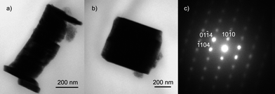 | ||
| Fig. 7 (a) TEM micrograph showing the cross-sectional area of a nanowire (3); (b) square projection nanotape (probably tilted at about 45°); (c) nanodiffraction pattern taken from a thin edge of the particle shown in (b) at zero tilt. | ||
TEM observations as shown in Fig. 5 and Fig. 7, together with SEM observations would appear to suggest that the wires exhibit a thin ribbon- or a tape-like morphology, as shown in Fig. 8. The thinnest dimension of the tapes is that parallel to the long c-axis, or in other words, the slowest growth is likely to occur perpendicular to the basal plane layers of the 2H structure. The long axis of the tapes is along ⅓〈20〉, while the wider dimension is along 〈010〉. It is interesting to note that the nanotapes appear to have a radically different morphology to the hexagonal symmetry of the 2H unit cell (i.e. to the hexagonal space group in which they crystallise). It seems likely that the formation of elongated tapes rather than hexagonal platelets is therefore driven by kinetic or materials supply factors in the synthesis and clearly cannot merely represent a thermodynamically preferred state. Uninhibited growth from a nucleation point in two (or three) dimensions would be expected to yield branched structures (by analogy to snowflakes) that propagate in all six equivalent directions. By contrast, growth from a surface would constrain such propagation to one direction only (by analogy to frost, for example, which also typically grows along ⅓〈20〉 directions). It should be noted that the nanotapes always grow from surfaces, so it is very likely that the tape morphology arises as a result of reaction and nucleation at the interface between the tantalum surface and a transported sulfur-containing phase. The evidence of TaS3 found at lower reaction temperatures combined with the fact that neither any metal (catalyst) particles were added nor were found at the tips or elsewhere of the nanotapes, would suggest that growth occurs via a vapour-solid (VS) process involving a sulfur-rich vapour phase and the tantalum foil surface. Such VS growth mechanisms have been proposed for a number of transition metal monosulfides,20 although in the SACVT experiments described herein, there is no evidence of the tip growth often induced by nanoparticular catalysts (which can often insinuate a vapour–liquid–solid, VLS, process). The accumulated evidence thus points to VS-mediated root growth of the nanotapes from the tantalum substrate surface.
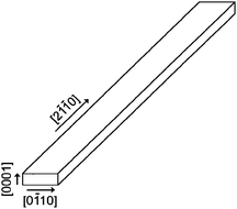 | ||
| Fig. 8 Schematic diagram of the morphology adopted by the TaS2 nanotapes (3). | ||
Considering the internal structure of the tapes, it was notable that a significant number of these exhibited a “fibrous” composition, as is exemplified by the nanotape shown in Fig. 9. The typical tape morphology is apparent, but dark-field images show that the sample is in fact composed of three parallel crystals aligned along the length of the wire. A combination of selected-area diffraction, nanobeam diffraction and dark-field imaging showed a few key points. First, all three of the component crystals in the tape grew parallel to [20], consistent with other results, but only the outer crystals had the [0001] orientation as the wire sat on the support (shown by the strong diffraction spots in Fig. 9d). Second, the weaker diffraction spots in this figure come from the central crystal and this appears to have an orientation close to [021]. Third, tapes of a similar nature that were composed of two or more nanocrystals with a fibrous morphology and a clear [20] fibre texture were also often observed. These observations would thus suggest that the nanotapes are predominantly, if not routinely, composed of smaller, fibrous single crystals and would suggest that the “bundling” of these smaller fibrils into nanotapes is part of a cooperative growth process. It remains to be established if this “bundling” process is key to the origins of enhanced superconductivity in the 2H-TaS2 nanotapes, although similar apparent effects have been described for semi-conducting boron carbonitride nanotubes, which become metallic on forming ordered bundles and also for metallic single walled carbon nanotubes, which on forming such arrays become superconducting.21,22 Equally, the suppression of charge density waves (CDW) in (bulk) layered dichalcogenides has been an important ingredient in the transition from semiconductivity to superconductivity. The progressive intercalation of copper in 2H-CuxTaS2 has demonstrated how superconductivity and CDW suppression in dichalcogenides is not only sensitive to carrier concentration and the density of states (DOS) but also and perhaps more importantly, to likely changes in the interaction between Ta–S layers and hence a disruption of the periodicity that induces CDWs.23 Similar relationships exist in the 2H-NaxTaS2 system24 and small variations in doping level have commensurate effects on the crystal structure (increases in unit cell volume and expansion along the c-direction and a measurable effect for CuxTaS2; 0 ≤ x ≤ 0.12 vs. an extremely subtle one in NaxTaS2; 0 ≤ x ≤ 0.1). In fact, a recent combined computational–single crystal experimental study of the electronic structure and properties of 2H-Cu0.03TaS2 compared to 2H-TaS2, demonstrates that on doping, the area of the Fermi surface increases (along with the value of EF and the number of charge carriers).25 While the DOS at EF decreases in 2H-Cu0.03TaS2 compared to 2H-TaS2, these factors have the combined effect of suppressing the CDWs (reducing the CDW transition temperature), and increasing the superconducting pairing (increasing Tc).
![Images of the internal structure of a nanotape composed of three parallel crystals: (a) Bright-field image; (b) dark-field image obtained using a reflection common to all crystals; (c) dark-field image obtained using a reflection unique to the outer crystals, leaving the central strand dark; (d) SAED pattern from this nanotape showing a superimposed diffraction pattern of both [0001] and [022̄1] components, together with some reflections generated by double diffraction. The diagonal streaking is a camera artefact from the overexposed transmitted beam.](/image/article/2010/NR/b9nr00224c/b9nr00224c-f9.gif) | ||
| Fig. 9 Images of the internal structure of a nanotape composed of three parallel crystals: (a) Bright-field image; (b) dark-field image obtained using a reflection common to all crystals; (c) dark-field image obtained using a reflection unique to the outer crystals, leaving the central strand dark; (d) SAED pattern from this nanotape showing a superimposed diffraction pattern of both [0001] and [021] components, together with some reflections generated by double diffraction. The diagonal streaking is a camera artefact from the overexposed transmitted beam. | ||
The ostensible connectivity between “chemical” and physical pressure (manifested as substitutionally induced modification of electronic structure, e.g. via hole doping) has been documented in high Tc cuprates (converting a Mott insulator ground state to a superconducting state). By loose analogy, pressure has been shown to suppress the CDW ground state in 1T-TaS2 to induce superconductivity.11 Similar pressure-induced effects were observed over a decade ago in the 6R polytype of TaS2 where Tc could be elevated from 2.3 K at ambient pressure to >4 K at 17.3 kbar.19 Just as with doping in 2H-Cu0.03TaS2, an increase in pressure in 6R-TaS2 was proposed to increase the area of the Fermi surface and an increase in Cooper pairs. An analogous effect may also be responsible for the observation of elevated Tcs in nanowires and nanotubes of NbSe226 for which electronic structure calculations have predicted a high DOS at the Fermi level (dominated by Nb 4d states).27 Importantly, similar calculations have predicted broadly equivalent effects for nanostructured 2H-TaS2 and the likelihood of superconductivity.28 At present the experimental band structure and DOS of TaS2nanostructures are unknown. A systematic investigation of the crystal chemistry, electronic structure and transport (and magnetic) properties of individual and bundled dichalcogenide nanowires is essential if we are to establish the equivalent structure-property relationships that are now emerging among the superconducting bulk chalcogenides. An understanding of growth and structure at the nanoscale is a vital first step towards this and to an ability to design chalcogenide nanowires with predictable properties.
Experimental section
In a typical reaction, elemental powders of tantalum (99.9%, −325 mesh, Aldridge) and sulfur (99.5%, Fisher) were ground together in a 1 : 2 molar ratio and sealed in a 12 mm diameter silica tube under a vacuum of 4 × 10⁻⁵ Torr. The tube was modified to accommodate a central constriction effectively dividing the ampoule into two sections (Fig. 10). One region (I) was filled with the reactant powders, the other (II) contained a piece of tantalum foil (10 × 30 × 0.25 mm, 99.9%, Aldridge).12 The tube was placed horizontally in a box furnace and heated, first to 115 °C to ensure vaporisation of sulfur and then to temperatures ranging from 400–1100 °C for 60–70 h (Table 1).| Sample number | Dwell temperature/°C |
|---|---|
| 1 | 400 |
| 2 | 500 |
| 3 | 650 |
| 4 | 750 |
| 5 | 900 |
| 6 | 1100 |
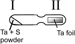 | ||
| Fig. 10 Schematic diagram of the reaction ampoule, indicating the two discrete sections of the tube. | ||
The ampoules were subsequently air-quenched to room temperature and opened. Powders in region I remain physically separated from products grown on the surface of the foil in region II. The latter were mechanically harvested from the foil and retained for analysis. Powder X-ray diffraction, (PXD), analysis was carried out using a Siemens D5000 powder diffractometer in Bragg–Brentano, flat-plate geometry. Nanowire samples from region II were loaded onto a flat glass disk using a double-sided circular carbon tab, normally used for attaching scanning electron microscopy (SEM) samples to aluminium stubs. Diffraction data were collected between 5° ≤ 2θ ≤ 80° as a step scan with a 0.02° step size over a scan time of 12 h with the sample stage rotating at 15 rpm. High anisotropy and resulting preferred orientation (coupled with crystallite size broadening effects) generally lead to variable quality results from PXD analysis of nanofibrous samples. Many alternative methods of loading samples were attempted with best results obtained from the method described above. PXD data were compared with calculated patterns generated from literature structural data using POWDERCELL and indexed using DICVOL.29,30
SEM was performed using a Philips XL30 ESEM. Samples were loaded onto aluminium stubs using adhesive carbon tabs and imaged in high vacuum mode with an applied 20 kV accelerating voltage and a working distance of 10 mm for energy dispersive X-ray analysis, (EDX). EDX analysis was performed using an Oxford instruments EDX spectrometer in order to determine elemental compositions (which can be obtained with accuracy for elements of atomic number from carbon upwards). Characterisation viatransmission electron microscopy (TEM) comprised bright- and dark-field imaging, together with selected-area electron diffraction (SAED) and was performed using a FEI Tecnai T20 (FEI Company, Eindhoven, Netherlands) operated at an accelerating voltage of 200 kV. For most measurements, samples were dispersed in isopropanol, and applied dropwise onto a holey carbon film supported on a 300 mesh copper grid. In separate experiments, samples were aligned in the microscope to attempt to image a cross-section of the anisotropic nanowires. For these sample preparations (encapsulations), silicon wafer sheets of 0.6 mm thickness were cut into 10 × 5 mm tabs and cleaned by sonicating in ethanol for 1 min. Epoxy resin infused with nanowires was used to bind the wafers together to form sandwiches which were ground down using wet and dry paper, such that the wafer sandwiches could be arranged vertically in the centre of titanium encapsulation holders (Technoorg Linda, Budapest, Hungary; Fig. 11a). The bound wafers were then ground (with the wafer/epoxy sandwich in a vertical position) until the sandwich (containing the sample) was flush with the surfaces of the flat sample holder (a thickness of ca. 80 µm). Dimpling from both sides using a Gatan dimple grinder with 4 µm diamond paste to a depth of 35 µm gave a central region of about 10 µm thickness which was further thinned using a precision ion polishing system, (PIPS) until a small hole first appeared in the centre of the wafer sandwich as shown in Fig. 11b. Images and diffraction patterns for all TEM experiments were recorded using an attached SIS Megaview III CCD camera (Olympus Soft Imaging Solutions GmbH, Münster, Germany). Diffraction patterns were simulated using the Desktop Microscopist software package (Lacuna Laboratories, formerly of Beaverton, Oregon, USA.
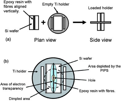 | ||
| Fig. 11 (a) Schematic of a silicon wafer/epoxy resin sandwich as it is loaded into the titanium sample holder prior to grinding flat for TEM; (b) plan view of an encapsulated sample prepared for a typical TEM experiment to image the cross-section of nanowires. | ||
Magnetic measurements were performed using a Quantum Design MPMS 5T SQUID magnetometer. Samples (∼20 mg) were loaded into degassed gelatine capsules. Field cooled (FC) and zero field cooled (ZFC) measurements with an applied field of 10 Oe between 1.8–20 K. All magnetic data were corrected for the gelatine capsules and for core diamagnetism.
Conclusions
The synthesis of TaS2 nanotapes has been achieved by a simple one-step reaction from elemental powders viaSACVT methods in a controllable and reproducible manner. Investigations into the varying composition, structure and morphology of tantalum sulfides with synthesis temperature in SACVT reactions have demonstrated that trisulfide nanomaterials (TaS3) are obtained at low temperature (e.g. 500 °C) in preference to the disulfidenanostructures seen at 650 °C and above. These reactions at 500 °C produce TaS3nanoribbons with high width-to-thickness ratios and powder XRD patterns that do not correspond to the monoclinc form of TaS3. Higher reaction temperatures produce nanotapes, fine nanowires and platelets of TaS2 respectively as the temperature increases and the disulfide progresses through a 2H to 1T phase transition in the process. The nanostructures formed at 650 °C are superconducting below 4 K and TEM confirm that these have the form of nanotapes with ⅓〈20〉 long axes, and [0001] as the narrow tape direction. Further SAED shows unequivocally that the nanotapes are of the 2H polytype, grow in the <20> direction and are composed of many smaller fibrils that propagate cooperatively. The modified coupling of Ta–S layers in these nanotapes compared to bulk 2H-TaS2 is likely to be at the heart of the enhanced superconductivity observed in the nanostructured disulfide.
Acknowledgements
DHG thanks the EPSRC for a studentship for CWD and WestCHEM for supporting this work. The authors thank Colin How for help with microscopy and Brian Miller for assistance with specimen preparation.References
- R. R. Chianelli, E. Prestridge, T. Pecorano and DeNeufville, Science, 1979, 203, 1105 CAS.
- R. Tenne, L. Margulis, M. Genut and G. Hodes, Nature, 1992, 360, 444 CrossRef CAS.
- S. Iijima, Nature, 1991, 354, 56 CrossRef CAS.
- C. N. R. Rao, F. Deepak, G. Gundiah and A. Govindaraj, Prog. Solid State Chem., 2003, 31, 5 CrossRef CAS.
- M. Remškar, Adv. Mater., 2004, 16, 1497 CrossRef CAS.
- F. Jellinek, J. Less Common Met., 1962, 4, 9 CrossRef.
- F. J. Di Salvo, B. G. Bagley, J. M. Voorhoeve and J. V. Waszczak, J. Phys. Chem. Solids, 1973, 34, 1357 CAS.
- P. Blaha, J. Phys.: Condens. Matter, 1991, 3, 9381 CrossRef CAS.
- S. Nagata, T. Aochi, T. Abe, S. Ebisu, T. Hagino, Y. Seki and K. Tsutsumi, J. Phys. Chem. Solids, 1992, 53, 1259 CrossRef CAS.
- J. A. Wilson, F. J. DiSalvo and S. Machajan, Adv. Phys., 1975, 24, 117 CAS.
- B. Sipos, A. F. Kusmartseva, A. Akrap, H. Berger, L. Forró and E. Tutiš, Nat. Mater., 2008, 7, 960 CrossRef CAS.
- C. W. Dunnill, H. K. Edwards, P. D. Brown and D. H. Gregory, Angew. Chem., Int. Ed., 2006, 45, 7060 CrossRef CAS.
- H. E. Swanson and E. Tatge, National Bureau of Standards, 1953, 539, 1 Search PubMed.
- B. E. Warren and J. T. Burwell, J. Chem. Phys., 1935, 3, 6 CrossRef CAS.
- A. Meerschaut, L. Guemas and J. Rouxel, J. Solid State Chem., 1981, 36, 118 CAS.
- X. Wu, Y. Tao, Y. Hu, Y. Song, Z. Hu, J. Zhu and L. Dong, Nanotechnology, 2006, 17, 201 CrossRef CAS.
- A. Meetsma, G. A. Wiegers, R. J. Haange and J. L. De Boer, Acta Crystallogr., Sect. C: Cryst. Struct. Commun., 1990, 46, 1598 CrossRef.
- M. Nath and C. N. R. Rao, J. Am. Chem. Soc., 2001, 123, 4841 CrossRef CAS.
- E. Figueroa, Y.-K. Kuo, A. Olinger, M. A. Lloyd, L. D. Bastin, S. Petrotsatos, Q. Chen, B. Dobbs, S. Dev, J. P. Selegue, L. E. DeLong, C. P. Brock and J. W. Brill, J. Solid State Chem., 1995, 114, 486 CrossRef CAS.
- J. P. Ge, J. Wang, H. X. Zhang and Y. D. Li, Chem.–Eur. J., 2004, 10, 3525 CrossRef CAS.
- X. Blase, J.-C. Charlier, A. De Vita and R. Car, Appl. Phys. Lett., 1997, 70, 197 CrossRef CAS.
- M. Kociak, A. Y. Kasumov and S. Gueron, Phys. Rev. Lett., 2001, 86, 2416 CrossRef CAS.
- K. E. Wagner, E. Morosan, Y. S. Hor, J. Tao, Y. Zhu, T. Sanders, T. M. McQueen, H. W. Zandbergen, A. J. Williams, D. V. West and R. J. Cava, Phys. Rev. B: Condens. Matter Mater. Phys., 2008, 78, 104520 CrossRef.
- L. Fang, Y. Wang, P. Y. Zou, L. Tang, Z. Xu, H. Chen, C. Dong, L. Shan and H. H. Wen, Phys. Rev. B: Condens. Matter Mater. Phys., 2005, 72, 014534 CrossRef.
- X. Zhu, Y. Sun, S. Zhang, J. Wang, L. Zou, L. E. DeLong, X. Zhu, X. Luo, B. Wang, G. Li, Z. Yang and W. Song, J. Phys.: Condens. Matter, 2009, 21, 145701 CrossRef.
- M. Nath, S. Kar, A. K. Raychaudhuri and C. N. R. Rao, Chem. Phys. Lett., 2003, 368, 690 CrossRef CAS.
- V. V. Ivanovskaya, A. N. Enyashin, N. I. Medvedeva and A. L. Ivanovskii, Phys. Stat. Sol., 2003, 238, R1 CAS.
- A. N. Enyashin, I. R. Shein, N. I. Medvedeva and A. L. Ivanonskii, Internet Electron. J. Mol. Des., 2005, 4, 316 Search PubMed http://www.biochempress.com/ .
- G. Nolze and W. Kraus, Powder Diffr., 1998, 13, 256.
- A. Boultif and D. Louer, J. Appl. Crystallogr., 2004, 37, 724 CrossRef CAS.
Footnote |
| † Electronic supplementary information (ESI) available: Magnetic susceptibility data for 3. See DOI: 10.1039/b9nr00224c |
| This journal is © The Royal Society of Chemistry 2010 |