Transmission electron microscope observation of a freestanding nanocrystal in a Coulomb potential well†
Sheng-Yong
Xu
*a,
Wei-Qiang
Sun
a,
Meng
Zhang
a,
Jian
Xu
b and
Lian-Mao
Peng
a
aKey Laboratory for the Physics and Chemistry of Nanodevices, Department of Electronics, Peking University, Beijing 100871, China. E-mail: xusy@pku.edu.cn
bCenter for Nanoscale Science, Department of Engineering Science and Mechanics, Pennsylvania State University, University Park, PA 16802-6300, USA
First published on 21st October 2009
Abstract
Usually pure electrostatic charges cannot be utilized alone to form macro-sized three-dimensional electromagnetic traps for trapping charged particles. These traps need additional dynamic electromagnetic fields. We report here the observation of a CdSenanocrystal floating over a carbon film in a transmission electron microscope. The nanocrystal was most likely trapped in a naturally formed, nanometre-sized 3D Coulomb potential well. The results indicated the possibility of developing a novel nanodevice for the trapping and manipulation of charged nanoparticles.
1. Introduction
At the micrometre and larger scales, optical tweezers, working with a gradient force toward the focal point of a laser beam due to the radial gradient of the beam intensity, have proven to be a powerful manipulation technique for a variety of subjects, from cooling and trapping atoms in a vapor, to trapping and manipulating large biological molecules, internal parts of cells and even living cells.1–3Magnetic tweezers, using magnetic beads that attach to the samples under test, have also been successfully applied in various measurements of biomaterials like DNA.4,5By further reducing the length scale to the nanometre range, the strength of Coulomb interaction between two charged particles is much larger than the gravitational interactions these particles receive from the Earth. For example, a 10 nm-diameter nanoparticle with a moderate density of 5 g cm−3 roughly weighs 10−20 N, but the Coulomb force between two unit charges separated at a space of 10–100 nm is 10−14–10−12 N, 6–8 orders of magnitude larger than the former. Further down to the atomic and molecular scales, the gravitational interactions are more negligible, and the electromagnetic interactions are dominant even in “neutral” atoms. In fact, each and every single atom (neutral or charged) in a solid is restricted in a localized, three-dimensional (3D) Coulomb potential well (CPW) formed by its neighboring atoms. It is well known that interactions between two neutral atoms can be qualitatively characterized by the Lennard-Jones potential:  , where r is the spacing between two atoms, and σ and ε are atom-dependent constants. This potential originates from Coulomb interactions between charge carriers, i.e., electrons and nuclei, of the two atoms. The potential is strongly repulsive at distance shorter than σ, and is attractive at large r, with a minimum around r = 1.1σ. Here the effective length scale of this potential is characterized by σ, which is usually at the order of 0.1 nm. Such localized Coulomb interactions at the atomic and molecular scales have been utilized to construct “molecular tweezers” in molecular engineering and self-assembly.6,7
It is then interesting to ask: Can one make electrostatic 3D CPWs to trap charged nanoparticles at the nanometre scale? The charge configurations in a natural solid could not be easily reproduced at the nanometre or larger scales. By Earnshaw's theorem, in a charge-free electrostatic field there is no point of stable equilibrium, or a CPW. Therefore, to trap a charged particle with a 3D CPW, one needs to construct more complicated charge distributions with some dynamic factors. Some successful examples of 3D CPWs consisting of dynamic electromagnetic fields are the Paul trap–AC quadrupole trap, which utilizes tailored high-frequency electrical fields to trap charged particles,8 and the Penning trap, where charged particles are trapped in a combination of electrostatic and magnetic fields.9 These traps, some of which have been applied in storage of fast ions and mass spectrometry,10–12 are typically on the macroscale where the gravitational interactions can not be fully neglected. However, recently Segal and Shapiro proposed theoretically that it is possible to construct a nano-sized Paul trap using four nanotubes for trapping single electrons.13
In this paper we report the transmission electron microscopy (TEM) observation of a CdSenanoparticle levitating and rotating randomly over a carbon film. By analyzing the underlying trapping mechanism, we concluded that the nanocrystal was most likely trapped in a naturally formed 3D CPW, however, with a trapping mechanism different from those reported previously.
2. Experimental details and results
The levitation and rotational motion of the CdSenanocrystal was observed in a 200 kV Jeol 2010F field-emission TEM in a study on high-intensity electron beam (HIEB) nano-welding and cutting of nanomaterials.14 The CdSenanocrystal samples were synthesized following the method developed by Qu and Peng15 and were stored in toluene solutions. For TEM investigation, the nanocrystals in toluene were spread on copper grids covered with a lacey-carbon-film, and dried in air. These nanocrystals had an average diameter around 10 nm. Under high magnification, they sat still on the supporting carbon film, and showed clear lattice spacings that belong to the CdSe zinc blende lattice with a = 0.605 nm.Surprisingly, one of the thousands of CdSenanocrystals under observation did not sit still on the carbon film. Instead, it rotated slowly, with a random rotation speed averaging at around one revolution per second, and kept on changing its rotation axis randomly. Since the TEM was not equipped with a video camera, we recorded a series of more than thirty high-resolution images of this nanocrystal with a CCD camera (see the ESI† ). The time window for capturing each image was 0.1 s, and the duration between two consecutive captures ranged from several seconds to half a minute. Figs. 1(a)–(i) are selected TEM images of this nanocrystal. In each image, a recognizable feature on the supporting carbon film is marked with blue dashed lines, and the central point of the nanocrystal in the first image, Fig. 1(a), is highlighted in the rest of the images as a reference for the relative shift of the nanocrystal center. Frequently seen lattice fringes in these images have spacings of 0.31 ± 0.01, 0.22 ± 0.01, and 0.19 ± 0.01 nm, matching to the lattice spacings of {200}, 0.303 nm, {220}, 0.214 nm and {113}, 0.182 nm, of the CdSe zinc blende structure where a = 0.605 nm. The nanocrystal shown in Fig. 1 continued to rotate randomly for more than 10 min, until it was finally burnt away by a focused electron beam with diameter of 10 nm and beam density of 105A cm−2.
 | ||
| Fig. 1 (a)–(i) TEM images of a CdSenanocrystal floating over a supporting carbon film on a copper grid. The nanocrystal rotated slowly, changing its rotation axis randomly for over 10 min. The same features on the supporting carbon film and the nanocrystal center of in the first image are highlighted with blue dashed lines and a yellow dot, respectively, in each image for reference. | ||
One can see from Fig. 1 that the shape of the nanocrystal continued to change, as did the in-plain orientation of certain lattice fringes. Indeed these images are the projections of the same nanocrystal along different observation directions, after the random rotation of the nanocrystal. If any part of the nanocrystal was connected to the supporting carbon film, when it rotated randomly, it would “roll” along the carbon film and change its central position remarkably. For this 10-nm-diameter particle, one turn of pure “rolling” motion results in a shift of around 30 nm of the particle center. However, this was not what we observed. By comparing the central position to the relatively fixed features on the supporting carbon film, as marked with blue dash lines in Figs. 1(a)–(i), we carefully measured the relative lateral shifts of the nanocrystal in each image with respect to its original center as shown in Fig. 1(a). The results are plotted in Fig. 2. During the whole period of observation, the centre of this nanocrystal only shifted slightly, within 1 nm from its original position.
 | ||
| Fig. 2 A plot of the in-plane position shift of the nanocrystal center shown in Figs. 1(a)–1(i), with respect to the original center of the nanocrystal in Fig. 1(a). During the floating and rotating motions of the nanocrystal over 10 min, its central position shifted slightly from its original position by less than 1 nm. | ||
Therefore, we can conclude unambiguously that it was actually floating freely over the supporting carbon film.
3. Discussion
This is a surprising conclusion. How can a 10-nm-diameter nanocrystal float over a supporting film? No matter how strange it seems, the nanocrystal was trapped in an unexpected potential well, a 3D trap.As stated previously, at the nanometre scale, electromagnetic interactions are dominant and gravitational interactions are negligible. However, the possible trap here does not seem to match the known electromagnetic traps. Under the conditions of observation, the possible 3D trap should not be the Paul trap which needs high-frequency (usually in MHz range) electrical fields with specially tailored shapes. Neither is it likely to be a Penning-type trap that results from a combination of electrostatic and magnetic fields, because the mass center of the observed nanocrystal stayed almost still, and there should be no current flow in this nonmagnetic, semiconducting nanoparticle, thus there should be no observable interactions between the nanoparticle and the magnetic fields in the TEM. And, the trapping mechanism does not resemble that of magnetic tweezers, which require that the target being trapped has a magnetic moment, e.g., from an attached magnetic bead.4,5 Therefore, a possible answer to the puzzling observation shown in Fig. 1 is that the CdSenanocrystal had been trapped in a naturally formed 3D CPW.
One can easily construct 1D and 2D CPWs with proper distributions of static charges, where Earnshaw's theorem does not work. In a 1D system, the simplest CPW can be made of only two separate unit charges. As shown in the inset of Fig. 3(a), two unit charges of the same sign, Q1 and Q2, are fixed at x = 0 and x = 1 µm, respectively. Fig. 3(a) illustrates the Coulomb potential energy for a third unit charge C located between x = 0 and x = 1 µm, where C has the same sign to Q1 and Q2. The Coulomb potential energy curve U(x) has an equilibrium point in the middle of the two charges, thus charge C can be trapped in such a simple CPW. The depth of the CPW is in the order of meV near the equilibrium point. Fig. 3(b) shows another simple 1D CPW, where two point charges, Q1 of −2e and Q2 of e, are fixed at x = 0 and x = 1 µm, respectively. For a third charge C of e located at x > 1 µm, the Coulomb potential energy U(x) has an equilibrium point at W (x ≈ 3.41 µm), and thus charge C can be trapped in this CPW, where the depth is in the order of 0.01 meV near the equilibrium point.
 | ||
| Fig. 3 Coulomb potential energy curves of two simple 1D electrostatic traps, where the corresponding charge distribution is shown in each inset. (a) Two unit charges of the same sign located at x = 0 and x = 1 µm, respectively, form a CPW for a third unit charge of the same sign, where the Coulomb potential energy has a stable equilibrium at x = 0.5 µm. (b) Two negative unit charges and one positive unit charge are located at x = 0 and x = 1.0 µm, respectively, forming a CPW for a third positive unit charge, with the stable equilibrium located at the point near x = 3.41 µm. | ||
Fig. 4 demonstrates a simple CPW in a 2D system. Charge Q1 of 2Ne is fixed at (0,0) in a 2D plane described by r–θ, and charge Q2 of −1Ne is located on a ring of r = R. When N is large enough, the charge Q2 can be roughly considered uniformly distributing on the ring of r = R. For negative charges their Coulomb potential energy has equilibrium at the location of ring with r ≈ 1.31R. Fig. 4 plots the Coulomb potential energy of a particle with a unit charge of −evs. its distance to Q1 in this configuration, where Q1 = 20e, Q2 = −10e, and R = 1 µm.
 | ||
| Fig. 4 Coulomb potential energy curve of a simple 2D CPW. As shown in the inset, charge Q1 of 20 e is fixed at (0,0), and charge Q2 of −10 e is uniformly distributed on a ring of r = 1.0 µm. They form a 2D CPW for negatively charged particles outside the ring of Q2. The stable equilibrium points are located at a ring with diameter r ≈ 1.31 µm. | ||
In the 3D case, where the Earnshaw's theorem works, one cannot construct 3D CPWs with simple distributions of electrostatic point charges. Referring to the situation of a solid, e.g., a cubic piece of salt crystal, the distribution of charges that are carried by electrons in each Na and Cl atom, are indeed not static but dynamic. We suggest that the naturally formed 3D CPW which trapped the CdSenanocrystal shown in Fig. 1 was formed by unique distributions of electrostatic charge on the supporting carbon film and the nanocrystal, where these two distributions were correlated to each other.
To check this conjecture, we propose here a simple model of the charge distributions and the correlation. The coordinates of the model are such that the electron beam in the TEM is running along the z-axis, and the supporting carbon film of the TEM grid is located in the xy-plane. The CdSenanocrystal of charge q is located at a position W of (0,0,L). Static charges on the carbon film are distributed in two coaxial rings that parallel to the xy-plane, ring 1 and ring 2 of radii of r1 and r2, (r1 < r2), and centers at (0,0,0) and (0,0,−d0), respectively. They are uniformly charged with positive Q1 = 2πλ1r1, and negative Q2 = 2πλ2r2, as schematically shown in Fig. 5, with densities per unit length of λ1 and λ2, respectively. When the nanoparticle with a positive charge q is moving along the z-axis, at the position of (0,0,z), the Coulomb potential energy of this particle in the two-ring system is given by
 | (1) |
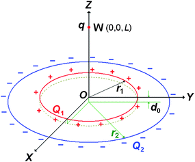 | ||
| Fig. 5 Schematic diagram of possible charge distribution that can result in a 3D Coulomb potential well at the location (0,0,L). Positive charge Q1 is fixed in the plane of z = 0 and uniformly distributed in a ring of radius r1 which is centered at (0,0,0). Negative charge Q2 is uniformly distributed in a ring in the plane z = −d0, where the ring is centered at (0,0,−d0) and has a radius r2. A positive charge of q is placed at the point W(0,0,L). Assume that when q changes its position from W(0,0,L) to W′(0,0,L + ΔL) by perturbation, it could lead to a slight change in the position of Q2, from the plane at z = −d0 to z = −(d0 + Δd), and Δd = αΔL, where α is a small constant. Then, mathematically the charge q can be trapped in a 3D CPW near the position W with suitable choices of Q1, Q2, r1, r2, q, d0 and α. | ||
Adjust the parameters of r1, r2, λ1 and λ2, one can find a position W at (0,0,L) where  and
and  . Therefore, the position of (0,0,L) is a potential minimum along the z-axis. If the nanoparticle moves slightly from (0,0,L) to (x,0,L), the Coulomb potential energy becomes
 | (2) |
However, when the parameters of r1, r2, λ1 and λ2 are chosen so as to form a CPW along the z-axis at W(0,0,L), the same point is always not the CPW minimum in the xy-plane, and vice versa. This is consistent with the Earnshaw's theorem.
Now we introduce a key assumption. Suppose that the location of Q1 is fixed, while the location of Q2 allows a slight motion. Since Q2 and q are attractive to each other, when the charge particle changes its position from W(0,0,L) to W′(0,0,L + ΔL) by perturbation, it leads to a slight change in the position of Q2, from the plane at z = −d0 to z = −(d0 + Δd) as the interaction between q and Q2 is getting weaker. Further assuming that Δd is approximately proportional to ΔL by Δd = αΔL, and α is a small coefficient constant, then mathematically we can find many sets of suitable parameters of r1, r2, Q1, Q2, q and α that result in 3D CPWs at the location W (0,0,L), where the Coulomb potential energy U(x,y,z) strictly satisfies  ,
,  ,
,  ,
,  ,
,  , and
, and  . Fig. 6 shows an example of such a Coulomb potential energy well, where r1 = 80 nm, r2 = 144 nm, q = e, Q1 = 40e, Q2 = −160e, d0 = 0 nm, and α = 0.16. The stable equilibrium point of this Coulomb potential energy well is located at (0,0,25 nm), where the depth is in the order of 0.1 meV, both along z-axis and in xy-plane near the equilibrium point. Note that the depth and shape of Coulomb potential energy wells constructed by the model in Fig. 5 is sensitive to the ratios of r2/r1, Q2/Q1, and α. Fig. 7 demonstrates that slight variations of these parameters may cause remarkable changes in shapes and depths of the corresponding Coulomb potential energy wells along the x-axis.
 | ||
| Fig. 6 Coulomb potential energy curves along the z-axis (left panel) and x-axis (right panel), respectively, of the two-ring charge distribution model described in Fig. 5, where q = e, Q1 = 30e, Q2 = −120e, r1 = 80 nm, r2 = 144 nm, α = 0.16, and d0 = 0 nm. The stable equilibrium point of the CPW is located at (0,0,25 nm). | ||
 | ||
| Fig. 7 Coulomb potential energy curves along the x-axis as a function of distance from the minimum point of CPWs resulting from the model shown in Fig. 6, under different parameters. Here for all these configurations, q = e, Q1 = 100e, r1 = 10 nm, and d0 = 0 nm. (a) For these CPWs Q2/Q1 = −4 and α = 0.16, and the variable parameter the ratio of r2/r1, from 1.79 to 1.81. (b) For these CPWs r2/r1 = 1.8 and α = 0.16, while the value of Q2/Q1 is varied from −3.95 to −4.05. (c) Q2/Q1 = −4, and r2/r1 = 1.80 are kept constant, while the value α is varied from 0.15 to 0.17. | ||
Comparing the charge distributions modeled in Fig. 5 and the real situation as shown in Fig. 1, the spacing d0 between the centers of the two charged rings could be caused by a thin insulating layer of residual material in the toluene solution of the CdSenanocrystals. The charges on ring 1 and ring 2 could be distributed on this residual insulating layer and the underneath carbon film, respectively. The slight up-and-down motion of the charges in ring 1 along the z-axis could result from sort of a vibration mechanism of the residual insulating layer on the carbon film.
We have calculated that the electron beam in our TEM observation does not greatly affect the trapping effect of the proposed 3D CPWs shown in Figs. 5–7. Assume the electron beam has a radial Gaussian intensity distribution: 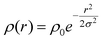 , where ρ0 is the intensity at the beam center, r is the radial distance to the beam center, and σ is a constant parameter so that a centralized cylinder of diameter 3σ contains most electrons in the beam. This radial Gaussian intensity results in an intensity gradient from the beam center to the edge, thus creating a net radial force on a positively charged particle towards the beam center. However, this additional Coulomb potential energy of unit charge is calculated to be around 10−4 meV, which is three orders of magnitude lower than that shown in Figs. 6–7 and therefore it is negligible.
On the other hand, the electron beam might have offered driving force for the rotational motion of the CdSenanocrystal as shown in Fig. 1. Here we give a rough estimation of the magnitude of this driving force. The moment of inertia I of the CdSenanoparticle is given by:  , where ρ is the mass density, R is the radius. If the nanoparticle starts from a stationary status and then rotates N turns in a period of T, its angular acceleration β can be roughly estimated from:
  . The torque that needs to make this angular acceleration is given by: M = Iβ. Taking T ≈ 1s, N ≈ 2, ρ ≈ 6 g cm−3 and R ≈ 5 nm, we get
  . Then the required driving force is roughly given by: F ∼ M/R ∼ 10−27 kg m s−2. Note that this required driving force is three orders of magnitude smaller than the gravity force on the same nanoparticle. We suggest that this tiny driving force is introduced from the incident electron beam by the following mechanism: When the electron beam passes through the target CdSenanocrystal, it loses part of its kinetic energy through various inelastic scattering processes with the target particle, thus causing a net pressure on the particle. When the shape and crystal structure of the particle is not perfectly symmetric, one side of the particle may scatter more electrons than the other side. Consequently, unbalanced angular momenta at the two sides leads to a net torque that causes rotational motion of the particle.
Also, the charges in the trapped CdSenanocrystal shown in Fig. 1 could be separated, forming a dipole-like distribution. By further simulation we may be able to figure out different models to reveal how the nanocrystal was trapped. In the meantime, we are not able to reveal the exact details of how such a 3D trap was naturally formed.
4. Conclusion
At the nanometre scale the strength of Coulomb interactions between charged particles is much larger than that of the gravitational interactions acting on these particles. We have reported here the TEM observation of a CdSenanocrystal floating over a carbon film, where the nanocrystal was most likely trapped in a naturally formed 3D Coulomb potential well (CPW). We have discussed the charge distributions for such a CPW trap. The results indicate the possibility of developing novel “nano-electro-tweezers” for the trapping and manipulation of charged nanoparticles, e.g., bio-macromolecules.Acknowledgements
We thank Y. B. Gao for valuable discussions. This work was supported by the NSF of China (Grant No. 10774002) and MOST of China (Grant No. 2006CB932401).References
- A. Ashkin, Proc. Natl. Acad. Sci. U. S. A., 1997, 94, 4853–4860 CrossRef CAS.
- D. G. Grier, Nature, 2003, 424, 810–816 CrossRef CAS.
- K. Dholakia, P. Reece and M. Gu, Chem. Soc. Rev., 2008, 37, 42–55 RSC.
- T. R. Strick, J. F. Allemand, D. Bensimon, A. Bensimon and V. Croquette, Science, 1996, 271, 1835–1837 CrossRef CAS.
- S. H. Leuba, T. B. Wheeler, C. M. Cheng, P. R. LeDuc, M. Fernández-Sierra and E. Quiñones, Methods, 2009, 47, 214–222 CrossRef CAS.
- F. K. Klärner and B. Kahlert, Acc. Chem. Res., 2003, 36, 919–932 CrossRef.
- M. Parac, M. Etinski, M. Peric and S. Grimme, J. Chem. Theory Comput., 2005, 1, 1110–1118 CrossRef CAS.
- W. Paul, Rev. Mod. Phys., 1990, 62, 531–540 CrossRef CAS.
- L. S. Brown and G. Gabrielse, Rev. Mod. Phys., 1986, 58, 233–311 CrossRef CAS.
- L. H. Andersen, O. Heber and D. Zajfman, J. Phys. B: At., Mol. Opt. Phys., 2004, 37, R57–R88 CrossRef CAS.
- M. Dahan, R. Fishman, O. Heber, M. Rappaport, N. Altstein, D. Zajfman and W. J. van der Zande, Rev. Sci. Instrum., 1998, 69, 76–83 CrossRef CAS.
- K. G. Bhushan, S. C. Gadkari, J. V. Yakhmi and V. C. Sahni, Rev. Sci. Instrum., 2007, 78, 083302 CrossRef CAS.
- D. Segal and M. Shapiro, Nano Lett., 2006, 6, 1622–1626 CrossRef CAS.
- S. Y. Xu, M. L. Tian, J. G. Wang, J. Xu, J. M. Redwing and M. H. W. Chan, Small, 2005, 1, 1221–1229 CrossRef CAS.
- L. H. Qu and X. G. Peng, J. Am. Chem. Soc., 2002, 124, 2049–2056 CrossRef CAS.
Footnote |
| † Electronic supplementary information (ESI) available: 21 TEM images of the same CdSenanocrystal taken at the same location. In each image a recognizable feature on the supporting carbon film is marked with blue dashed lines; the nanocrystal center in the first image is marked with a green dot as the reference; and the nanocrystal center in each of the remaining images is highlighted with a yellow circle. See DOI: 10.1039/b9nr00144a |
| This journal is © The Royal Society of Chemistry 2010 |