Microfluidic probe: a new tool for integrating microfluidic environments and electronic wafer-probing†
David A.
Routenberg
and
Mark A.
Reed
*
Department of Electrical Engineering, Yale University, New Haven, CT, USA. E-mail: mark.reed@yale.edu
First published on 29th October 2009
Abstract
We demonstrate a new tool for integrating microfluidic channels with commonly used electronic probing techniques. The “microfluidic probe” allows rapid and repeatable fluidic and electronic addressing of small die sites on a variety of substrate types without the need for permanent modification or dicing of the device wafers. We also use the probe to demonstrate locally patterned chemical modification of a substrate. The probes are easily fabricated using standard soft-lithography and basic machining making this a widely accessible technique for electronics and fluidics researchers.
Introduction
Integrating a microfluidic addressing scheme with electronic measurement systems, as is required for interrogating field-effect bio-molecular sensors1–3 or other micro- and nano-electronic devices, presents a unique set of challenges. At the very least, a useful integration scheme should be compatible with common electronic contacting methods like wire-bonding or wafer-probing. Additional challenges include reducing the die size to increase yield and thus decrease device cost, as well as avoiding permanent modification of the device wafers, which would preclude further device fabrication steps after initial fluidic testing. Such steps might include deposition of dielectric layers for surface passivation, selective removal of such passivation layers, or metallization to reconnect certain devices in various circuit integration schemes. These challenges have not been addressed fully by any of the existing microfluidic techniques and as such, no single method has been accepted universally for use with electronic biosensors or other hybrid electronic/fluidic applications.2,4–9The most commonly used approaches rely on one of the following four methods: a temporary “stick-on” approach, where a molded polymer layer, usually polydimethylsiloxane (PDMS), is temporarily affixed to the surface of the wafer,1,3,4,10,11 a permanently bonded glass or polymer layer that contains the channels and input and output ports,4,12,13 a clamp-type method where a specifically sized substrate is placed into a device that mechanically forces it against a sealing gasket,4,14 or an open reservoir attached to the top surface of the chip.2 For the “stick-on” devices the chip size is dictated by the area required to provide sufficient adhesion to yield a reliable seal and is usually 1 cm2 or larger. Permanently bonded approaches may yield smaller die size but require irreversible modification of the substrate and thus preclude further device fabrication steps. The clamp-type methods are also irreversible as they require dicing the wafers into specifically sized chips to fit into the clamp and further, they are often incompatible with electronic measurements. Finally, the open reservoir method requires manual pipetting and thus is very time-consuming with many opportunities for human error.
It would be useful to have a method for temporarily forming a microfluidic channel at the surface of a non-diced substrate with a small contact area that would allow increased device density while remaining compatible with standard electronic probing techniques, and would preserve the ability to perform additional fabrication steps on the substrate after initial fluidic testing, if required. Further, the setup time should be quick, and the technique should be accessible to anyone with access to standard soft-lithography capabilities.
Here we present a new device that we refer to as the “microfluidic probe” because of its analogous form and function to that of a typical electrical wafer probe. This device allows for non-permanent, non-destructive, microfluidic addressing of small regions of a wafer or chip while preserving the ability to simultaneously use standard electronic wafer-probing techniques. We demonstrate the use of microfluidic probe devices with both micropositioner-type single-tip wafer probes as well as multi-tip probe cards such as those used in automated wafer probers. Finally we use a “microfluidic probe” with a network of arbitrarily shaped channels to reproduce specific patterns of chemical functionality on a wafer. Each of these techniques provides an easy-to-use tool for use in the electronics laboratory that requires little additional equipment or time-consuming sample preparation. The “microfluidic probes” are durable enough to be reused many times, but easy enough to fabricate to be disposable if necessary for preventing cross-contamination. Together, these properties make the “microfluidic probe” an ideal tool for addressing electronic biosensors. As an example, we apply this to previously demonstrated silicon nanowire FET biosensors, demonstrating dramatically improved ease of use and throughput over prior manual fluidic approaches. In addition, we believe that the microfluidic probe approach should also be useful for a wide variety of other microfluidic applications.
Methods
Device overview
The general principle of the device can be seen from the photograph in Fig. 1a, which shows a “microfluidic probe” being used on a manual wafer probe station. The probe is used in a fashion analogous to an electrical needle probe, whereby, using a micropositioner, it is brought into mechanical contact with the wafer to form a sealed channel. | ||
| Fig. 1 Overview of “microfluidic probe” concept: (a) fully assembled probe in use on manual probe station with planar substrate. The microfluidic probe is the top structure, with a top metal support ring (through which tubing with dyed solution (pink) emerge), and an underlying polystyrene holder and PDMS molded region (with two dye solution channels). The probe is touching a wafer with fabricated dies (visible in the background). A reflection of the probe is seen on the wafer (inverted). Two electrical probes come in from the left and right (reflections also visible). (b) Schematic cross-section of probe for planar substrates—bottom surface of PDMS contains recessed channel and surrounding gasket. (c) Cross-section of probe for substrates with buried channels—bottom surface contains two gaskets. (d) Cross-section of probe for substrates patterned with ridges to form channel walls—bottom surface is not patterned. | ||
Fluids enter and exit through tubing attached to the top of the probe. Because there is no need to permanently bond the probe tip to the wafer or to rely on self-adhesion, the contact area need only be slightly larger than the desired fluidic channel itself. This allows the electrical contact pads to be placed much closer together than in the previous “stick-on” method and allows at least a 10-fold reduction in chip area.
Depending on the nature of the substrate and the experiment, the user may wish to employ flow channels either completely formed by the molded PDMS probe tip or they may wish to use the probe as an interface to previously fabricated buried channels on the substrate or to partially formed channels defined by raised ridges on the substrate. Each of these cases is shown schematically in Fig. 1. To demonstrate the applicability of the microfluidic probe to each of these situations, we produce a variant of the device to contact each of these types of substrates.
Fabrication of the microfluidic probes
The “microfluidic probe” consists of a piece of PDMS elastomer molded or cut into the shape of an inverted truncated pyramid, of which the bottom surface is patterned using standard soft-lithography techniques. The PDMS portion of the device is bonded to a polystyrene support layer, which is in turn attached to a micropositioner via a machined steel support arm. The fabrication of each variant in Fig. 1 is nearly identical with the exception of the soft-lithographic patterning of the bottom surface of the PDMS. We will specifically describe the fabrication process for the variant shown in Fig. 1b, used for planar substrates.A master mold is prepared by a two-layer photolithographic process using SU-8, a negative photoresist, as shown in Fig. 2a. A 5 mm thick layer of Sylgard 184 (Dow Corning) PDMS is cast using the mold to form a recessed channel surrounded by a protruding gasket as shown in Fig. 2b. The depth of this recessed channel has been fabricated as high as 500 μm to accommodate turbulent flow which may significantly decrease biosensor response time.2,15 In the case of the buried channel variant, the channel and gasket are replaced by two round gaskets (Fig. 2c) that interface with the inlet and outlet of a buried channel on the substrate (Fig. 2e). In the case of the third variant, no molding of the PDMS is necessary to interface with the ridges on the substrate.
 | ||
| Fig. 2 Details of PDMS probe tips and substrates: (a) SU-8 mold for PDMS; (b) PDMS layer for planar substrate probe with recessed channel surrounded by raised gasket; (c) probe for buried channels with two circular gaskets; (d) flat bottomed probe for substrates with channel walls; (e) buried channel formed on substrate from SU-8, inset shows cross-section and (f) SU-8 ridge forms channel walls on substrate, inset shows cross-section. | ||
The pyramidal PDMS layer is plasma bonded to a 2 mm thick square of polystyrene (PS) to provide a rigid support for mounting the probe and attaching tubing. Prior to bonding, inlet and outlet holes are drilled in the polystyrene. After plasma bonding, holes are cored through the PDMS to provide an inlet and outlet to the channel. The holes are placed at each end of the recessed channel (Fig. 2b), or a single hole is cored for each round gasket (Fig. 2c). For the third variant, the holes are positioned on the flat bottom (Fig. 2d) such that they will be contained within the channel walls defined by the ridge on the substrate (Fig. 2f). PTFE tubing is inserted into the holes in the polystyrene and secured with epoxy and the entire assembly is affixed to the steel support arm as shown in Fig. 1a.
To demonstrate the effectiveness of each variant of the microfluidic probe we prepared substrates with both buried channels and raised ridges corresponding to Fig. 1c and d in addition to the planar substrates that are typically used for bio-sensing experiments. The buried channels and raised ridges were both formed in SU-8 by the methods described in ESI†. Examples of these substrates are shown in Fig. 2e and f.
Operation and characterization
In the typical mode of operation, the microfluidic probe is positioned over the region of interest on the chip and then lowered by adjusting the micropositioner until the PDMS contacts the surface and is slightly deformed, indicating that a temporary seal has been formed. The solution is then driven through the channel by a syringe connected to the input tube. The flow may also be driven by applying a vacuum to the output tube. After use, the channel is flushed by blowing nitrogen or compressed air through the input to clear the fluid before lifting the probe and proceeding to the next die or test site. Videos of fluid flow through each type of channel are shown in the ESI†.Each type of microfluidic probe was pressure tested with water to determine the maximum internal pressure before leakage occurred. As expected, the burst pressure depended on the extent to which the PDMS layer was deformed by pressing it against the substrate. We measured the burst pressure as a function of the downward force exerted by the micropositioner. We clamped the output tube of the probe and placed the substrate on an electronic balance, which allowed direct measurement of the micropositioner force (assuming the compliance of the balance is large with respect to all other elements). We measured the input force on the syringe and calculated the pressure in the fluidic channel, assuming zero flow and thus constant pressure. In each case the maximum pressure was found to vary linearly with the micropositioner force. The results of this test are summarized in Table 1. Each of the probe types was patterned exactly as shown in Fig. 2 and the downward forces were varied from 1g to 25g. Each type of probe was found to be able to withstand an internal pressure of at least 60 kPa before leaking. Further optimization of the gasket design may provide an increase in burst pressure. While the burst pressures for the fluidic probes are significantly lower than the typical burst pressure for a permanently bonded or clamped structure,14 they are sufficient to establish the high flow rates needed for sensing applications.
| Planar substrate | Buried channels | Channel walls | |
|---|---|---|---|
| a Maximum pressure was measured when gaskets were completely compressed for planar and buried channel substrates. For substrates with channel walls, manipulator force was set equal to that used for planar substrate, normalized by contact area. b Slope and intercept were determined from linear fit of burst pressure vs. force applied to probe. | |||
| Maxa/kPa | 63.4 | 84.5 | 83.9 |
| Slopeb/kPa g−1 | 1.0 | 7.4 | 4.2 |
| Interceptb/kPa | 10.3 | 7.3 | 0 |
In addition to using the fluidic probe with a manual wafer probe station, we integrated it into a Cascade Summit 12K automated wafer prober to demonstrate its efficacy in a high throughput system. This system uses a 32 pin probe card to simultaneously contact all the pads on a 3 mm × 3 mm die.
The pins on the probe card form a ring and we attach a fluidic probe to the probe card so that the PDMS portion of the probe protrudes into the center of the ring as shown in Fig. 3. The bottom edge of the PDMS is positioned just below the tips of the pins so that it is deformed slightly to form a seal when the pins are brought into contact with the substrate surface.
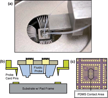 | ||
| Fig. 3 (a) Microfluidic probe integrated with electronic probe card in automated wafer prober; (b) schematic cross-section and (c) die photo showing pad-frame and fluidic probe contact area. | ||
Applications

In this case the fabrication differs slightly to accommodate channel patterns that are narrower than the diameter of the syringe needle used for coring the inlet and outlet holes. The full process details are given in ESI†. The device is shown schematically in Fig. 5a. The arbitrarily shaped channels are molded in a 100–200 µm thick layer of PDMS. The mold also contains pillars that protrude through the entire thickness of the PDMS, producing through holes to access the channels from the top side of this layer. The channels and through holes are visible in Fig. 5b. A second PDMS layer, 5 mm thick, is molded with an array of fan-out channels to connect the closely spaced through holes to a set of holes drilled in a PS supporting layer. Finally the thin PDMS layer is bonded to the PDMS–PS assembly so that the patterned channels connect to the fan-out channels. This assembly is shown in Fig. 5c. The PTFE tubing is inserted into the holes in the PS and the entire assembly is mounted on a micropositioner as before.
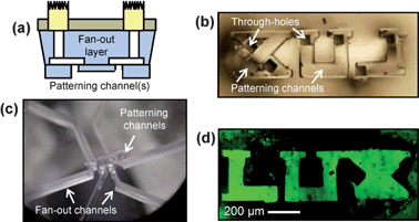 | ||
| Fig. 5 (a) Schematic cross-section of patterning probe; (b) patterned channels and through holes; (c) fan-out connects to patterning channels and (d) resulting pattern on substrate after selective area functionalization. | ||
As a demonstration, we use this patterning tool to selectively functionalize the surface of a glass slide with a fluorescent label in an arbitrary pattern. Clean glass slides are treated with 3-aminopropyltriethoxysilane (APTES), 1% in toluene, for 1 h to yield an amine terminated surface. The patterning probe is then applied to the surface of the slide using the micropositioner. A buffer solution containing fluorescein isothiocyanate (FITC), a green fluorescent label, is then briefly flowed through each of the channels, where it is bound by APTES. The channels are flushed with fresh buffer to remove any unbound molecules of FITC. The channels are then cleared with nitrogen and the probe is removed from the surface. Fluorescent imaging reveals a patterned layer of the fluorescent label corresponding to the channel pattern, as shown in Fig. 5d. The patterned functionality has feature fidelity down to the few microns scale (notice the serifs in the “L” and “U” letters). The fluorescent patterning is just one example of many surface modifications that could be performed using a similar technique.
Conclusions
We have demonstrated the “microfluidic probe,” a new device for temporary, local microfluidic addressing of substrates. We have shown its applicability to a variety of substrate types and specifically to nanowire FET sensor measurements. The device integrates easily into commonly used electrical probing systems and allows die sizes to be reduced to a few square mm. Integration into automated probing systems enables high throughput, wafer-scale fluidic measurements and significant statistical sampling that is impractical for other hybrid approaches. Because the microfluidic probe devices can be fabricated easily by standard soft-lithography techniques, they should be accessible to many researchers wishing to combine microfluidic and electronic measurements. Further, due to the flexibility afforded by the lithographic patterning process, we have shown that arbitrarily patterned probes can be used for “molecular contact printing.” This technique, when integrated into an automated system, enables flexible substrate patterning and selective area functionalization or chemical processing.Acknowledgements
This work was supported by the National Institutes of Health (R01EB008260).Notes and references
- F. Patolsky, G. F. Zheng and C. M. Lieber, Nat. Protocols, 2006, 1, 1711–1724 CAS.
- E. Stern, J. F. Klemic, D. A. Routenberg, P. N. Wyrembak, D. B. Turner-Evans, A. D. Hamilton, D. A. LaVan, T. M. Fahmy and M. A. Reed, Nature, 2007, 445, 519–522 CrossRef CAS.
- T. Pui, A. Agarwal, F. Ye, N. Balasubramanian and P. Chen, Small, 2009, 5, 208–212 CrossRef CAS.
- P. Abgrall and A.-M. Gue, J. Micromech. Microeng., 2007, 17, R15 CrossRef.
- H. Becker and C. Gärtner, Anal. Bioanal. Chem., 2008, 390, 89–111 CrossRef CAS.
- D. Erickson and D. Li, Anal. Chim. Acta, 2004, 507, 11–26 CrossRef CAS.
- G. S. Fiorini and D. T. Chiu, BioTechniques, 2005, 38, 429–446 CrossRef CAS.
- S. Haeberle and R. Zengerle, Lab Chip, 2007, 7, 1094–1110 RSC.
- S. K. Sia and G. M. Whitesides, Electrophoresis, 2003, 24, 3563–3576 CrossRef CAS.
- H. Bang, W. G. Lee, J. Park, H. Yun, J. Lee, S. Chung, K. Cho, C. Chung, D.-C. Han and J. K. Chang, J. Micromech. Microeng., 2006, 16, 708 CrossRef CAS.
- C. Dalton and K. V. I. S. Kaler, Sens. Actuators, B, 2007, 123, 628–635 CrossRef.
- C. S. Martinez-Cisneros, N. Ibanez-Garcia, F. Valdes and J. Alonso, Anal. Chem., 2007, 79, 8376–8380 CrossRef CAS.
- H. Muhlberger, H. Wonhee, A. E. Guber, V. Saile and W. Hoffmann, IEEE Sens. J., 2008, 8, 572–579 CrossRef.
- C. R. Tamanaha, M. P. Malito, S. P. Mulvaney and L. J. Whitman, Lab Chip, 2009, 9, 1468–1471 RSC.
- T. M. Squires, R. J. Messinger and S. R. Manalis, Nat. Biotechnol., 2008, 26, 417–426 CrossRef CAS.
- D. J. Lockhart and E. A. Winzeler, Nature, 2000, 405, 827–836 CrossRef CAS.
- R. K. Smith, P. A. Lewis and P. S. Weiss, Prog. Surf. Sci., 2004, 75, 1–68 CrossRef CAS.
- L. Yan, X.-M. Zhao and G. M. Whitesides, J. Am. Chem. Soc., 1998, 120, 6179–6180 CrossRef CAS.
Footnote |
| † Electronic supplementary information (ESI) available: Fabrication processes and experimental details are included as well as movies depicting the operation of the microfluidic probe on each type of substrate. See DOI: 10.1039/b913912e |
| This journal is © The Royal Society of Chemistry 2010 |