All-inorganic quantum-dot light-emitting devices formed via low-cost, wet-chemical processing†
Benjamin S.
Mashford
a,
Tich-Lam
Nguyen
a,
Gerard J.
Wilson
b and
Paul
Mulvaney
*a
aSchool of Chemistry & Bio21 Institute, University of Melbourne, Parkville, Victoria 3010, Australia. E-mail: mulvaney@unimelb.edu.au
bCSIRO Molecular and Health Technologies, Bag 10, Clayton South, Victoria 3169, Australia
First published on 5th August 2009
Abstract
The fabrication and characterisation of solution-processed, all-inorganic light-emitting devices incorporating colloidal CdSe/ZnS quantum dots are presented. Using sol–gel synthetic routes, highly luminescent core–shell QDs are embedded between spin-coated p-type NiO and n-type ZnO charge-transport layers. The resulting devices show pure QD electroluminescent emissions with a maximum EL brightness of 249 cd m−2.
Introduction
A high intensity, inexpensive light-emitting device (LED) incorporating colloidal quantum dots (QDs) is an optoelectronic component that would be very attractive to those working in the field of display technologies. Established colloidal synthetic routes to QD formation have been shown to yield QD materials with both a high quantum efficiency and a low degree of particle polydispersity. These properties may ultimately allow a QD-LED with an emission wavelength that is tunable by using QDs of the desired size and which possesses the high-quality spectral properties inherent to QDs. Several recent reports1,2 of QD-LEDs describe structures that include organic charge-transport layers, deposited in layered arrangements very similar to those used in organic light-emitting devices (OLEDs). More recently, Caruge et al. reported the development of a sputter-coated NiO layer as a hole-transport layer (HTL) in a QD-LED.3,4 The use of robust, inorganic charge-transport materials is desirable because they are expected to allow higher operating currents and to be less susceptible to the problems that beset organic semiconductors.5 However, to achieve the ultimate goal of ‘printable electronics’, it is highly desirable that vacuum-chamber deposited layers are avoided entirely. We report here on the electroluminescence from an all-inorganic QD-LED that uses solution-processed nanocrystalline charge-transport layers. Like solution-processed OLED deposition, the simplicity and low-cost of this technique naturally lends itself to applications requiring large-scale materials deposition, such as in the manufacture of flat-screen displays.Experimental
Processing of NiO layers
The NiO sol–gel precursor was prepared by dissolving nickel acetate tetrahydrate (Aldrich) in methanol to a concentration of 0.4 M. An equimolar quantity of diethanolamine (Aldrich) was added under stirring to improve sol stability and the substrate wettability of the resulting thin film. Solutions prepared in this manner have been noted to remain stable for several months. ITO slides (15–20 Ω −1) were cleaned by successive ultrasonic treatment in detergent, purified water, acetone and propanol before drying under nitrogen. Thin films were prepared by spin-coating the sol–gel precursor onto ITO slides under ambient conditions at a spin speed of 3000 rpm for 30 s. Samples were then placed immediately into a tube furnace and annealed under air at 425 °C for 10 min, forming a dense, polycrystalline material. Film thicknesses were measured by a stylus profiler to be 30–40 nm thick.Processing of quantum dot layers
Separately, CdSe/ZnS core–shell QDs were synthesised by adapting methods recently reported in the literature.6–8 The 4.8 nm CdSe cores were capped with 4 monolayers of ZnS. The resulting core–shell particles had an emission peak at 621 nm and were 7.6 nm in diameter. To achieve the highest quality QD films, it was found that multiple washing steps were necessary to minimise the amount of excess ligand in the spin-coated film. The QDs were washed via precipitation with acetone and centrifugation before being redispersed into chloroform. This procedure was repeated 6–8 times. Finally, the QDs were dispersed into hexane before they were deposited onto the NiO via spin-coating at 2000 rpm, forming a film approximately 40 nm in thickness.Processing of ZnO layers
ZnO nanoparticles were synthesised via a simple, low-temperature base-catalysed procedure.9 Briefly, zinc acetate dihydrate (Aldrich) was dissolved in ethanol heated at 50 °C under stirring to form a 0.02 M solution. Once fully dissolved, an equimolar amount of methanolic tetramethylammonium hydroxide (TMAH) was added dropwise over 2 min, leading to the immediate formation of ZnO nanoparticles. After cooling, the nanoparticles were washed via precipitation in hexane and centrifuged, before being redispersed in fresh propanol to a concentration of 16× that of the original solution. ZnO thin films were deposited by spin-coating at 2000 rpm before heating at 100 °C for 2 min to evaporate the solvent. This procedure yielded transparent, nanocrystalline films 30–40 nm in thickness.Device fabrication
Ag cathodes with an area of 1 mm2 were deposited through a shadow mask via thermal evaporation in an Emitech K950X vacuum evaporator at an operating pressure of 1 × 10⁻⁴ mbar. The thicknesses of the metal electrodes were measured to be in the range of 50 to 60 nm.Spectroscopic studies
Optical characterisation of thin film materials was performed on a Cary 5 UV-vis-NIR spectrometer and on a Jobin–Yvon Fluorolog spectrofluorimeter. PL and EL spectra were acquired on an Acton Microspectrometer attached to an Olympus microscope. All absorption measurements were made of samples deposited on quartz substrates. Estimates of the NiO valence band energy were determined with a Riken AC-2 photoemission spectrometer while the conduction band position was estimated from the measured optical band gap.Structural characterisation
X-Ray diffraction measurements were made on a Bruker D8 Advance diffractometer fitted with a graphite-monochromated copper tube source using CuKα filtered radiation. All film thickness measurements were made on a Veeco Dektak 150 stylus profiler. Characterisation of film surface roughness was performed on a Digital Instruments Atomic Force Microscope operating in tapping mode.Results and discussion
While sol–gel processing of conductive, metal-oxide semiconductor thin films has been widely applied to n-type materials such as n-ZnO10 and ITO,11 there have been far fewer reports of sol–gel derived p-type materials.12 In this report, we demonstrate a QD-LED that uses a transparent, conductive p-type NiO HTL that is fabricated via sol–gel synthesis. To the best of our knowledge, this is the first time that a sol–gel derived metal-oxide has been used for this purpose. There have, however, been a small number of reports of the use of sol–gel synthesised NiO thin films for electrochromic13 and transparent electronic applications.14 The QD-LED described in this work also employs an inorganic ETL formed from ZnO, an n-type semiconductor that has been demonstrated to facilitate electron injection into CdSe/ZnS QDs.15 The arrangement of the layers that form the QD-LED is illustrated in Fig. 1a. | ||
| Fig. 1 (a) Schematic diagram of ITO/NiO/QD/ZnO/Ag light-emitting device. (b) Energy level diagram of ITO/NiO/QD/ZnO/Ag light-emitting device. | ||
A key requirement for all thin film LED designs is a high degree of transparency of the anode. Although NiO is a wide-band gap semiconductor (Eg ≈ 3.7 eV), reported NiO thin film materials have rarely exhibited a visible-region transmittance as high as that predicted solely by the bulk band gap value. In addition, NiO is a material with widely studied electrochromic properties13,16 that allow reversible switching between transparent and coloured optical states depending on the electrochemical state of its surface. The absorption profile in Fig. 2a shows that our sol–gel synthesis yields NiO thin films that remain highly transparent throughout the visible spectrum, with a transmission of greater than 90% in the region where EL emissions are located. The strong increase in absorption in the UV region can be attributed to band gap transitions. From this profile, the absorption coefficient α was evaluated as a function of wavelength and used to determine the band gap energy Eg of our NiO material via the following relation:17
| αhν = (hν − Eg)m | (1) |
 | ||
| Fig. 2 (a) UV-VIS absorption profile of a 40 nm thick, sol–gel derived NiO film, annealed at 425 °C. The inset shows a plot of absorption coefficient vs. photon energy for the determination of the NiO optical band gap. (b) Variation in conductivity σ as a function of temperature T for sol–gel derived NiO. | ||
Although both direct and indirect band gap transitions have been reported in NiO,18 the clear linear relationship shown here (Fig. 1a, inset) indicates strong direct band gap transitions. Extrapolation of the linear section of this curve to zero absorption coefficient yields an estimated band gap of Eg = 3.77 eV.
In its pure, stoichiometric form NiO is highly insulating but there are several reports of NiO with varying degrees of p-type conductivity.18,19 Metal-oxide semiconductors formed by the sol–gel process are expected to contain a large number of defects and it is from these defects that conductivity in undoped NiO arises. Both nickel vacancies and interstitial oxygen in the NiO lattice lead to the presence of Ni3+ acceptor species.20
Measurements of the activation energy of sol–gel derived NiO help to determine the energetic depth of these acceptor states. Fig. 2b shows measured variations in the conductivity of NiO thin films with changing temperature. These yield the activation energy via the following relation:17
| σ = σ0e−Ea/kT | (2) |
 | ||
| Fig. 3 (a) XRD photoemission spectrum of a 40 nm thick, sol–gel derived NiO film indicating a valence band maximum energy of 5.4 eV. Inset shows XRD pattern of the same NiO film. (b) Tapping mode AFM image of a 40 nm thick, sol–gel derived NiO film deposited on cleaned ITO substrate, annealed at 425 °C. | ||
The colloidal QDs employed in the emissive layer of this QD-LED have a core of CdSe, over-coated with a 4 monolayer-thick ZnS shell. Particles with thicker shells were chosen for their high quantum yield and because of observations that the QDs maintained a high level of PL emissions even after repeated washing steps.
Since the QD-LED design used here has the ETL deposited over the QD particles, it is critical that its deposition does not adversely affect the integrity of the emissive layer. The emission from colloidal QDs is known to be greatly reduced by exposure to heated enviroments.22 Previous studies of QD PL have shown that the processing temperature should ideally be kept below 100–150 °C at all times to retain maximum QD emissions.22 The majority of published sol–gel syntheses of thin film ZnO involve higher annealing temperatures (above 400 °C) in air to convert the precursor materials to a transparent, polycrystalline thin film.10,23 There have, however, also been reports of alternative low-temperature routes for the synthesis of thin film ZnO that involves spin-coating colloidal ZnO nanocrystals from solution.24,25 This approach was recently demonstrated in a hybrid organic–inorganic QD-LED.15 The use of pre-formed ZnO nanocrystals offers greater compatibility with colloidal QD-LED fabrication because the only necessary thermal step required to form thin film ZnO is a brief heating to remove residual solvent. Charge transport through this nanoporous array of colloidal particles is expected to be less efficient than through fully densified ZnO but the experimental results presented here show that this material can still serve as an effective ETL. To allay concerns about unwanted removal of the QD particles by spin-coating on the ZnO ETL, the integrity of the emissive layer was checked via confocal microscopy. Uniform coverage of the QD particles on the substrate was observed even after deposition of the ZnO layer. Studies of the optical properties of this thin ZnO film indicate that the particles retain a high degree of surface-trap PL emission, characterised by a broad, visible-region fluorescence.26 This indicates that the ZnO nanoparticle surfaces have not undergone a large degree of sintering. From the absorbance spectrum shown in Fig. 4a, the average particle size can be inferred from published calibration data.9 With the measured shoulder peak location at 320 nm, we estimate the band gap to be 3.9 eV. This in turn gives an estimate of the average nanoparticle diameter to be 3.5 nm.9 A convenient way to monitor how the QD layer is affected by being placed in contact with the ETL and HTL components is to measure the PL yield at each step of the fabrication process. As shown in Fig. 4b, there is a significant reduction in PL emissions from the QD layer once it is deposited on the NiO-covered ITO. Since no significant physical or chemical changes to the QDs have taken place during this deposition step, this quenching is thought to be mainly due to an electronic interaction between the QDs and the hole-rich substrate on which it is in contact. A further reduction is also observed after spin-coating deposition of the ZnO ETL.
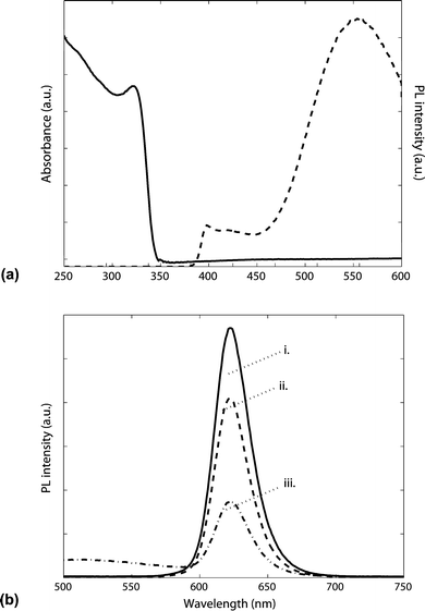 | ||
| Fig. 4 (a) Absorption profile (solid line) and PL spectrum (dashed line) of ZnO nanoparticles deposited on quartz substrate. PL excitation wavelength is 310 nm. (b) PL spectrum of a sample comprising (i) a 40 nm thick film of QDs on bare quartz substrate, (ii) QDs deposited on 40 nm NiO film, (iii) QDs deposited on 40 nm NiO and then over-coated with a 30 nm thick ZnO nanocrystal layer. | ||
Fig. 5a compares the PL and EL spectra from a QD-LED incorporating red-emitting QDs (PL peak position 622 nm). An examination of the PL signal from the final device reveals an emission profile that is dominated by the QDs but also shows significant contributions from the ZnO material. In comparison, the EL signal displays only QD emissions, with no visible contribution from the ZnO (neither UV exciton nor visible-region trap-state transitions). This is an indication that electron–hole recombination is occurring predominantly in the QD layer, as required for optimal device operation. The EL spectrum is slightly broadened and the peak position is red-shifted by approximately 10 nm, with respect to the PL spectrum. This observation is similar to that reported in other studies4 and is thought to be due to the strong electric fields incurred by use of resistive charge-injection layers. The electric field acts to reduce the energy of exciton recombination through the Stark effect.27 The I–V behaviour shown in Fig. 5b illustrates the improved performance in devices that include the ZnO ETL. Devices with the Ag cathode deposited directly onto the QD layer show a low emission intensity and an onset of naked-eye visible emission at approx. 3 V. This turn-on voltage drops to 2.2 V with the ZnO ETL included. This observation demonstrates that intermediate layers such as ZnO nanocrystals facilitate effective electron injection into the QD conduction band. Measurements of the EL emission intensity (Fig. 5c) yield a peak brightness of 249 cd m−2 at an applied operating bias of −8 V. The plot of luminous efficiency (Fig. 5c, inset) shows a maximum value of 0.014 cd A−1, which is quite low compared with other recently reported QD-LEDs and this is thought to largely result from the relatively high current density seen in the device.
 | ||
| Fig. 5 (a) PL (dashed line) and EL (solid line) spectra as measured from ITO/NiO/QDs/ZnO/Ag device. Peak PL position is located at 618 nm. EL peak position is located at 628 nm for device operation at −6 V. (b) Plot of current density vs. applied voltage for device incorporating 40 nm ZnO and for device without ZnO electron injection layer. (c) Measured luminous intensity vs. applied voltage for the two types of test QD-LEDs. The inset plots the luminous intensity vs. the current density. | ||
Conclusions
Inorganic QD-LEDs have been fabricated via wet-chemical deposition of nanocrystalline semiconductor layers under ambient conditions. The devices show very pure QD light emission and low turn-on voltages. The technique for fabricating sol–gel derived NiO described here provides a facile route to a highly conductive and chemically robust p-type layer, with an energy offset suitable for hole injection into CdSe/ZnS QDs. Although there remains significant work to optimise the performance of these devices, this design holds potential with regard to its inherent scalability and simplicity. The use of spin-coated inorganic layers provides QD-LEDs with the low-cost advantages of solution-deposited organic materials, while retaining the superior optical properties and chemical stability of semiconductor nanocrystal materials.Acknowledgements
B.S.M. acknowledges the receipt of an APA postgraduate scholarship and a CSIRO postgraduate studentship. P.M. acknowledges support through ARC Grant FF0561486.References
- Y. Li, A. Rizzo, R. Cingolani and G. Gigli, Adv. Mater., 2006, 18, 2545–2548 CrossRef CAS.
- J. Zhao, J. Zhang, C. Jiang, J. Bohnenberger, T. Basche and A. Mews, J. Appl. Phys., 2004, 96, 3206–3210 CrossRef CAS.
- J.-M. Caruge, J. E. Halpert, V. Wood, V. Bulovic and M. G. Bawendi, Nat. Photonics, 2008, 2, 247–250 Search PubMed.
- J.-M. Caruge, J. E. Halpert, V. Bulovic and M. G. Bawendi, Nano Lett., 2006, 6, 2991–2994 CrossRef CAS.
- A. P. Ghosh, L. J. Gerenser, C. M. Jarman and J. E. Fornalik, Appl. Phys. Lett., 2005, 86, 223501–223503 CrossRef.
- J. Jasieniak, C. Bullen, J. Van Embden and P. Mulvaney, J. Phys. Chem. B, 2005, 109, 20665–20668 CrossRef CAS.
- J. Jasieniak and P. Mulvaney, J. Am. Chem. Soc., 2007, 129, 2841–2848 CrossRef CAS.
- R. Xie, U. Kolb, J. Li, T. Basche and A. Mews, J. Am. Chem. Soc., 2005, 127, 7480–7488 CrossRef CAS.
- A. Wood, M. Giersig, M. Hilgendorff, A. Vilas-Campos, L. M. Liz-Marzan and P. Mulvaney, Aust. J. Chem., 2003, 56, 1051–1057 CrossRef CAS.
- H. Li, J. Wang, H. Liu, H. Zhang and X. Li, J. Cryst. Growth, 2005, 275, e943–e946 CrossRef CAS.
- M. J. Alam and D. C. Cameron, Thin Solid Films, 2000, 377–378, 455–459 CrossRef CAS.
- A. N. Banerjee and K. K. Chattopadhyay, Prog. Cryst. Growth Charact. Mater., 2006, 50, 52–105.
- P. A. Williams, A. C. Jones, J. F. Bickley, A. Steiner, H. O. Davies, T. J. Leedham, S. A. Impey, J. Garcia, S. Allen, A. Rougier and A. Blyr, J. Mater. Chem., 2001, 11, 2329–2334 RSC.
- Y. Ohya, H. Koyama, T. Ban and Y. Takahashi, Mater. Sci. Eng., B, 1998, 54, 55–59 CrossRef.
- J. W. Stouwdam and R. A. J. Janssen, J. Mater. Chem., 2008, 18, 1889–1894 RSC.
- G. Boschloo and A. Hagfeldt, J. Phys. Chem. B, 2001, 105, 3039–3044 CrossRef CAS.
- A. E. Jimenez-Gonzalez, J. A. Soto Urueta and R. Suarez-Parra, J. Cryst. Growth, 1998, 192, 430–438 CrossRef CAS.
- H. Kamal, E. K. Elmaghraby, S. A. Ali and K. Abdel-Hady, J. Cryst. Growth, 2004, 262, 424–434 CrossRef CAS.
- P. Puspharajah, S. Radhakrishna and A. K. Arof, J. Mater. Sci., 1997, 32, 3001–3006 CrossRef CAS.
- D. Adler and J. Feinleib, Phys. Rev. B: Solid State, 1970, 2(3), 3112–3134 CrossRef.
- G. Wantz, L. Hirsch, N. Huby, L. Vignau, J. F. Silvain, A. S. Barriere and J. P. Parneix, Thin Solid Films, 2005, 485, 247–251 CrossRef CAS.
- J. Jasieniak, J. Pacifico, R. Signorini, A. Chiasera, M. Ferrari, A. Martucci and P. Mulvaney, Adv. Funct. Mater., 2007, 17, 1654–1662 CrossRef CAS.
- V. Musat, B. Teixeira, E. Fortunato and R. C. C. Monteiro, Thin Solid Films, 2006, 502, 219–222 CrossRef CAS.
- C. Czekelius, M. Hilgendorff, L. Spanhel, I. Bedja, M. Lerch, G. Muller, U. Bloeck, D.-S. Su and M. Giersig, Adv. Mater., 1999, 11, 643–646 CrossRef CAS.
- E. A. Meulenkamp, J. Phys. Chem. B, 1998, 102, 5566–5572 CrossRef CAS.
- A. van Dijken, E. A. Meulenkamp, D. Vanmaekelbergh and A. Meijerink, J. Phys. Chem. B, 2000, 104, 4355–4360 CrossRef CAS.
- S. A. Empedocles and M. G. Bawendi, Science (Washington, D. C.), 1997, 278, 2114–2117 CrossRef CAS.
Footnote |
| † Electronic supplementary information (ESI) available: AFM images of NiO films on Si substrates. See DOI: 10.1039/b905256a |
| This journal is © The Royal Society of Chemistry 2010 |