Twinning mediated growth of ZnSe tri- and bi-crystal nanobelts with single crystalline wurtzite nanobelts as building blocks†
Lei
Jin
ab,
Jianbo
Wang
*a,
Shuangfeng
Jia
a,
Hongqian
Sang
a,
Liangzi
Deng
a,
Xue
Yan
a,
Yao
Cai
a,
Ping
Lu
a and
Wallace C. H.
Choy
*b
aDepartment of Physics, and Key Laboratory of Acoustic and Photonic Materials and Devices of Ministry of Education, and Center for Electron Microscopy, Wuhan University, Wuhan 430072, China. E-mail: wang@whu.edu.cn
bDepartment of Electrical and Electronic Engineering, University of Hong Kong, Pokfulam Road, Hong Kong, China. E-mail: chchoy@eee.hku.hk
First published on 5th October 2009
Abstract
A variety of ZnSe nanostructures, including the single-, bi- and tri-crystal nanobelts, are successfully fabricated through the thermal evaporation method and comprehensively investigated by a combination of various transmission electron microscopy (TEM) techniques. All nanostructures are of metastable wurtzite phase and the bi- and tri-crystal nanobelts are both mediated by the {01![[1 with combining macron]](https://www.rsc.org/images/entities/char_0031_0304.gif) 3} twinning, with the single crystal nanobelts as building blocks. Benefiting from the commonly observed morphological evolutions, not only the crystallographic relations for different variants in an individual bi- or tri-crystal nanobelt, but also the intrinsic connections between different morphologies are fully understood by selected area electron diffraction, convergent beam electron diffraction and high-resolution TEM techniques, which reveals that the accompanying formation of tri-crystal nanobelt, the {013} relationship, though maintained still, is not as strict as that in a bi-crystal nanobelt and holds a ∼0.75° deviation for a case study; the angles between adjacent twinning variants/planes are compressed from ∼125.0° in bi-crystal nanobelts to ∼120°, and finally form an asymmetric twinning plane distributions. The study helps deepen the understanding of tri-crystal and related complex semiconductor nanostructures.
3} twinning, with the single crystal nanobelts as building blocks. Benefiting from the commonly observed morphological evolutions, not only the crystallographic relations for different variants in an individual bi- or tri-crystal nanobelt, but also the intrinsic connections between different morphologies are fully understood by selected area electron diffraction, convergent beam electron diffraction and high-resolution TEM techniques, which reveals that the accompanying formation of tri-crystal nanobelt, the {013} relationship, though maintained still, is not as strict as that in a bi-crystal nanobelt and holds a ∼0.75° deviation for a case study; the angles between adjacent twinning variants/planes are compressed from ∼125.0° in bi-crystal nanobelts to ∼120°, and finally form an asymmetric twinning plane distributions. The study helps deepen the understanding of tri-crystal and related complex semiconductor nanostructures.
1 Introduction
Considerable efforts have been focused on the studies of quasi-one-dimensional (1D) nanostructures due to their unique properties. They are ideal building blocks in the potential applications in nano-optoelectronics, nano-sensors and nano-circuits.1–3 The properties of nanostructures are significantly influenced by their dimensions, shapes and microstructures.4–6 By introducing the twinning structures, it is expected that complex nanostructures, including two- and three-dimensional architectures, would be achieved via self-assembly of 1D building blocks.7 Novel applications might also emerge.ZnSe, a wide direct bandgap (2.67 eV at 300 K8) II–VI semiconductor, has been considered as a key material for the short-wavelength optoelectronic devices. Structurally, there are two extremely basic polytypes known as wurtzite (2H) and zinc blende (3C), respectively.9 The zinc blende based structures had been extensively studied and used for making light-emitting diodes and laser diodes since the 1990s,10,11 while the wurtzite counterpart was rarely focused on, mainly due to their thermodynamically metastable nature at room temperature.9 However, wurtzite ZnSe has a larger direct bandgap than that with a zinc blende structure, and is of lower symmetry thus allowing fewer glide systems.12,13 Therefore, it has been suggested that the performance may be improved by replacing the normally cubic with the hexagonal wurtzite.12 By applying different pressure and temperature, we have previously reported the phase-controlled growth of ZnSe nanostructures.14,15 A full picture has also been drawn to guide the vapor phase fabrications of metastable wurtzite materials,15 which provides the possibility to obtain the complex nanostructures with a certain phase.
Nanobelts (or nanoribbons) with tri-crystal morphology have been reported for ZnS,16,17 ZnSe18 and ZnCdSe19,20 where it is mentioned that two of the constituent nanoblades are mediated by the {013} twinning. Strictly speaking, in order to keep the tri-crystal morphology, the angle between any two twinning planes (TPs) should be strictly 120°. However, in a hexagonal wurtzite structure, i.e., a = 3.974 Å and c = 6.506 Å (JCPDS 80-0008) for ZnSe, the angle between (013) and (10![[3 with combining macron]](https://www.rsc.org/images/entities/char_0033_0304.gif) ) TPs equals 125° which is a 5° deviation from the ideal value. Therefore, how to accommodate this deviation is still an open question. Several models have been proposed to interpret the formation mechanism of the tri-crystal nanobelts and related nanostructures.16,18,19 However, no clear evidence shows experimentally the connectivity of the third blade.
) TPs equals 125° which is a 5° deviation from the ideal value. Therefore, how to accommodate this deviation is still an open question. Several models have been proposed to interpret the formation mechanism of the tri-crystal nanobelts and related nanostructures.16,18,19 However, no clear evidence shows experimentally the connectivity of the third blade.
To fully investigate this, we successfully fabricate bi- and tri-crystal nanobelts with single crystalline wurtzite nanobelts as building blocks and subsequently study the crystallographic relations between the constituent nanoblades as well as the intrinsic connections between different morphologies using various TEM techniques, which reveals that accompanied by the formation of a tri-crystal nanobelt, the {013} relationship, though maintained still, is not as strict as that in a bi-crystal nanobelt and holds a ∼0.75° deviation for a case study; the angles between adjacent twinning variants/planes are compressed from ∼125.0° in bi-crystal nanobelts to ∼120°, and finally form an asymmetric twinning plane distributions. The study helps deepen the understanding of tri-crystal and related complex semiconductor nanostructures.
2 Experimental
2.1 Synthesis
A horizontal double-zone tube furnace was utilized to synthesize the ZnSe nanostructures. About 0.5 g ZnSe powder (99.99% Sigma Aldrich) was loaded in an alumina boat and pushed into the high temperature zone (Zone I) as vapor source. The silicon (100) substrate, sputtered with ∼20 s of gold film, was placed downstream at the low temperature zone (Zone II). The furnace was then pumped to ∼0.04 Torr and purged with the carrier gas of highly purified argon premixed with 5% hydrogen at a stable rate of about 600 sccm (sccm denotes standard cubic centimeters per minute) to remove the residual oxygen. After 30 min, the flow rate of the carrier gas and the reaction pressure were maintained at 600 sccm and 50 Torr, respectively. Then the furnace was heated up for the subsequent growth and the temperatures in Zones I and II were 1000 and 800 °C, respectively. The whole growth lasted for 30 min.2.2 Characterization
A LEO-1530 field emission gun scanning electron microscope (SEM) was used for morphological analysis as overall information. The products were then scratched off the substrate and prepared for transmission electron microscopy (TEM) observation. Two kinds of TEM samples were prepared: one was sonicated in ethanol and then dropped onto the holey carbon-coated copper grid; the other was embedded and solidified in epoxy resin, then mechanically thinned and ion-milled by a Gatan precision ion polishing system PIPS691. TEM observations including bright field (BF) imaging, dark field (DF) imaging, selected area electron diffraction (SAED) and convergent beam electron diffraction (CBED) were performed using JEOL JEM-2010(HT) electron microscope, high resolution TEM (HRTEM) characterizations were taken on JEOL JEM-2010FEF(UHR) electron microscope equipped with a field emission gun and Ω-type in-column energy filter system. All microscopes were operated with an acceleration voltage of 200 kV.3 Results and discussion
3.1 Morphology
For a large scale observation, the morphology of the as-fabricated nanostructures is investigated by SEM, with the low magnification image shown in Fig. 1a. It has been observed that the yield of products is significantly improved in comparison with our preliminary study18 by means of increasing the flow rate of the carrier gas and decreasing the pressure of the reaction, which are expected to facilitate the evaporation and subsequent vapor transport of the ZnSe source.14,15 | ||
| Fig. 1 SEM images of the as-grown nanostructures under (a) low and (b) high magnifications. The arrowheads indicate the constituent nanoblades. | ||
The detailed morphology is further detected from the zoomed-in SEM image as presented in Fig. 1b, which demonstrates that the dominant product is the tri-crystal nanobelt. Each constituent nanoblade has been clearly observed as indicated by the arrowheads in Fig. 1b. Besides, a small number of single- and bi-crystal nanobelts have also been observed.
3.2 Microstructures and evolutions
Various TEM techniques, including the BF/DF imaging, SAED, CBED and HRTEM, are subsequently utilized for better understanding of the microstructures, the formation mechanism (section 3.3) and the crystallographic relations (section 3.4) of the constituent nanoblades, for convenience, through the sequence of single-, bi- and tri-crystal nanobelts.![[2 with combining macron]](https://www.rsc.org/images/entities/char_0032_0304.gif) 0}, which has been expected to be of the lowest surface energy, thus favoring room temperature stability.15
0}, which has been expected to be of the lowest surface energy, thus favoring room temperature stability.15
![(a) BF image of the single crystalline nanobelts and corresponding SAED patterns taken from the circular regions (b) b and (c) c in (a), respectively, showing the wurtzite nature of the nanobelts. (d) BF image of another nanobelt for CBED measurement. (e) Experimental and (f) simulated CBED patterns taken from the circular area in (d) projected along the [01̄10] axis, indicating the [0001] axis. The inset shows a nanoparticle located on the tip of a nanobelt, suggesting the VLS growth mechanism.](/image/article/2010/CE/b914542g/b914542g-f2.gif) | ||
| Fig. 2 (a) BF image of the single crystalline nanobelts and corresponding SAED patterns taken from the circular regions (b) b and (c) c in (a), respectively, showing the wurtzite nature of the nanobelts. (d) BF image of another nanobelt for CBED measurement. (e) Experimental and (f) simulated CBED patterns taken from the circular area in (d) projected along the [010] axis, indicating the [0001] axis. The inset shows a nanoparticle located on the tip of a nanobelt, suggesting the VLS growth mechanism. | ||
The asymmetric morphology, combined with the observed nanoparticle on the tip (inset of Fig. 2a), further indicates that the nanobelt forms through a two-dimensional growth: (i) Rapid growth upon the vapor-liquid-solid (VLS) mechanism23 along [301], a direction approximately perpendicular to the (302) plane, which differs from the previous wurtzite ZnSe nanostructures grown along [0001], <100> and <110> directions.12,24 (ii) Polarity induced secondary growth along ±[0001] directions resulting in the asymmetric final morphology. This asymmetric growth has been widely reported in semiconductor nanomaterials, such as ZnO, ZnS, etc.25,26
In view of the uniqueness of the c-axis in the hexagonal lattice and its importance to fully understand the crystallographic relations between different twinning variants in bi- and tri-crystal nanobelts, CBED technique is therefore utilized to determine this direction. Due to the following reasons: (i) the presence of ±(0001) secondary diffractions along [110] projection (Fig. 2b) inevitably leads to severe overlapping of the diffraction disks; (ii) diffraction intensities in (0002) and (000) disks under two-beam conditions are hard to distinguish from not only in the experimental results, but also in the simulated ones. We thus selected [010] axis for CBED measurement with the experimental and simulated results shown in Fig. 2e and f, respectively. The measurement was performed in the region marked with O in Fig. 2d and the simulation was calculated using the dynamical electron diffraction theory with a convergent angle of 10.42 mrad and a series of thickness. The best match was found at a thickness of 148 nm (Fig. 2f), which suggests that [0001] points to the teeth-like regions as indicated by the arrowhead in Fig. 2d.
Such orientation is reflected from the relative thickness mapping t/λp of the nanobelt (Fig. 3a), where t is the absolute thickness and λp is the mean free path of inelastic electron scattering,27 because the asymmetric growth inevitably results in the thinner thickness near the (0001)-edge. It is confirmed by the rapid drop at ∼250 nm in the thickness profile along b0b1 (Fig. 3b), in addition, profiles along c0c1 (Fig. 3c) and d0d1 (Fig. 3d) further reveal that the thicknesses at the saw-like and teeth-like areas are both homogeneous, which indicates steady growth.
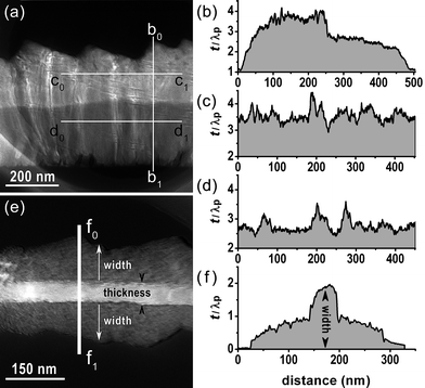 | ||
| Fig. 3 Relative thickness mappings of (a) a nanobelt and (e) a tri-crystal nanobelt and the corresponding thickness profiles along (b) b0b1, (c) c0c1, (d) d0d1 and (f) f0f1, respectively. | ||
21] axis (Fig. 4a), exhibits a nearly symmetric appearance along the dashed line between the constituent nanoblades denoted by I and II, respectively. Corresponding tilting series of SAED patterns has been indexed as a superimposition of two sets of diffraction patterns (as indicated by the blue and red frames) mediated by the (013) twinning and reveal the wurtzite nature of the bi-crystal nanobelt (Fig. 4b to 4d).
![BF images viewed along (a) [1̄1̄21] and (h) [1̄1̄20] directions showing the direction transformation between single- and bi-crystal nanobelt. Corresponding SAED patterns from the bi-crystal region projected along (b) [1̄1̄21], (c) [5̄2̄73] and (d) [3̄031] axes, indicating the {011̄3} twinning relation. SAED patterns taken from the region (e) e, (f) f and (g) g in (a) without any further tilting revealing nanobelt S and nanoblade II have the same crystallographic relations.](/image/article/2010/CE/b914542g/b914542g-f4.gif) | ||
Fig. 4 BF images viewed along (a) [21] and (h) [20] directions showing the direction transformation between single- and bi-crystal nanobelt. Corresponding SAED patterns from the bi-crystal region projected along (b) [21], (c) [![[5 with combining macron]](https://www.rsc.org/images/entities/char_0035_0304.gif) 73] and (d) [031] axes, indicating the {013} twinning relation. SAED patterns taken from the region (e) e, (f) f and (g) g in (a) without any further tilting revealing nanobelt S and nanoblade II have the same crystallographic relations. 73] and (d) [031] axes, indicating the {013} twinning relation. SAED patterns taken from the region (e) e, (f) f and (g) g in (a) without any further tilting revealing nanobelt S and nanoblade II have the same crystallographic relations. | ||
The twinning variants and the interfacial microstructures are further investigated at different scales (Fig. 5). The sharp (013) twinning boundary (TB), as illustrated by the BF/DF images in Fig. 5a to 5c, has been maintained down to the atomic level despite an extra displacement along the TB (see HRTEM image in Fig. 5e taken from the square region of Fig. 5d), which implies the strict twinning relationship between the constituent variants I and II.
 | ||
| Fig. 5 (a) BF and (b), (c) DF images of a bi-crystal nanobelt; (d) BF and (e) HRTEM images of another bi-crystal nanobelt showing the strict {013} twinning relationship. | ||
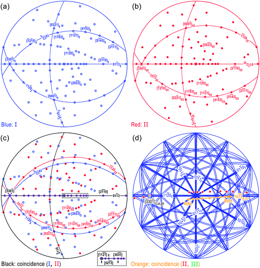
This relationship is consequently summarized in the composite stereographic projection (Fig. 6c), which is obtained by superimposition of projections from variants I and II (Fig. 6a and 6b) mediated by (013) twinning. The overall crystallographic relations are therefore fully understood, with part of the results listed as below:
(i) Besides the coincidence of (013) TP and related axes in the TP (for example, [11], [52![[7 with combining macron]](https://www.rsc.org/images/entities/char_0037_0304.gif) ], [30], etc), two parallel relationships with [000]I//[021]II and (110)I//(110)II are concurrently observed.
], [30], etc), two parallel relationships with [000]I//[021]II and (110)I//(110)II are concurrently observed.
(ii) Other relations such as [021]II/\[17![[8 with combining macron]](https://www.rsc.org/images/entities/char_0038_0304.gif) 3]II = 7.68° and [20]I/\[110]II ≈ 5.31°28 may be further used.
3]II = 7.68° and [20]I/\[110]II ≈ 5.31°28 may be further used.
(iii) The presence of (10)II plane helps to introduce the third nanoblade to finally form a tri-crystal nanobelt. Hence, a stereographic projection for tri-crystal nanobelt is also constructed as Fig. 6d. Further discussions will be carried out in section 3.4.
 | ||
| Fig. 6 Stereographic projections of (a) variant I, (b) variant II, (c) the bi-crystal nanobelt and (d) tri-crystal nanobelt. | ||
21] and [20] directions (Fig. 4a and h), unveiling the almost identical shapes between the nanoblades II and the nanobelt S (as indicated) despite their final widths. The typical SAED patterns in [21] zone axis are presented in Fig. 4e–g, which originate from regions e to g without any further tilting, respectively. The good consistence confirms that nanobelt S and nanoblade II also hold the same crystallographic orientations. Therefore, products with both similar morphologies and crystallographic orientations are treated as the same variant hereafter, and described by the same color (i.e., blue for I, red for II and green for III).
Aside from the bi-/single-crystal (Fig. 4a) and bi-/tri-crystal (inset of Fig. 7a) direct transformations, a continuous evolutional process has also been observed through single to bi-crystal then to tri-crystal morphology, as the BF image shown in Fig. 7a. The tri-crystal nanobelt which can simply be regarded as a bi-crystal base (i.e., I and II) plus the third nanoblade (i.e., III) has a length of several micrometers (Fig. S2),† extending from its tip (Fig. 7a) to the end as shown in Fig. 8a. Corresponding SAED patterns (Fig. 7b and c) and subsequent tilting series (Fig. 8b–h) recorded from the indicated single-, bi- and tri-crystal regions (Fig. 7a and 8a) structurally confirm this transformation and undoubtedly verify the above mentioned [000]I//∼[021]II relation upon the indexed and simulated SAED patterns in Fig. 7c and d, respectively. The characteristic (110)I,II diffraction spots keep coincidence indeed at the bi-crystal region, which is consistent with the stereographic projection (as depicted by the black arc in Fig. 6c) and reveals the strict twinning relation in bi-crystal nanobelt to a great extent.
 | ||
| Fig. 7 (a) BF image and corresponding SAED patterns taken from the (b) single crystal and (c) bi-crystal regions of (a) showing the continuous transformation. (d) Simulated SAED pattern for the bi-crystal region. | ||
![(a) BF image and corresponding SAED patterns of a representative tri-crystal nanobelt projected along (b) , (c) [033̄1], (d) [178̄3], (e) [257̄3], (f) [112̄1], (g) [415̄3] and (h) [303̄2] axes, respectively. The selected areas are marked by a dashed circle in (a). (i) BF image of another tri-crystal nanobelt from the embedded TEM sample projected along ∼[33̄01]. (j) BF image and corresponding DF images using (k) (2̄111)II, (l) (2̄110)I and (m) (1̄102̄)III beams (indicated by arrowheads k, l, m in (d)) as illuminating sources.](/image/article/2010/CE/b914542g/b914542g-f8.gif) | ||
Fig. 8 (a) BF image and corresponding SAED patterns of a representative tri-crystal nanobelt projected along (b)  , (c) [031], (d) [173], (e) [253], (f) [111], (g) [413] and (h) [302] axes, respectively. The selected areas are marked by a dashed circle in (a). (i) BF image of another tri-crystal nanobelt from the embedded TEM sample projected along ∼[301]. (j) BF image and corresponding DF images using (k) (111)II, (l) (110)I and (m) (10)III beams (indicated by arrowheads k, l, m in (d)) as illuminating sources. , (c) [031], (d) [173], (e) [253], (f) [111], (g) [413] and (h) [302] axes, respectively. The selected areas are marked by a dashed circle in (a). (i) BF image of another tri-crystal nanobelt from the embedded TEM sample projected along ∼[301]. (j) BF image and corresponding DF images using (k) (111)II, (l) (110)I and (m) (10)III beams (indicated by arrowheads k, l, m in (d)) as illuminating sources. | ||
Moreover, we found that the products can be etched with a long time immersion in alcohol (chemically pure) and leave the relics as shown in Fig. S3.† Though the crystal structures have collapsed, the outer shapes become more distinguished depicting each building block.
) twinning relation as the SAED patterns shown in Fig. 8b–h. Such relation has been maintained, without exception, for all observed samples. Therefore, it is reasonable to deduce that any two nanoblades in tri-crystal nanobelt are mediated by {013} twinning because of the random process for TEM sample preparation and subsequent observations. Actually, the (013) twinning has been verified for nanoblades I and II in Fig. 7b. Moreover, several extra diffraction spots are observed, all of which can be attributed to the double diffraction resulting from variants I and II (or III). No appreciable zinc blende cores can be detected under the present experimental conditions.
The cross section of a tri-crystal nanobelt has successfully been obtained in the embedded TEM sample (Fig. 8i). The projection is close to along [301]. By respectively selecting the (111)II, (110)I and (10)III diffraction beams (as indicated by arrowheads k, l, m in Fig. 8d) for DF imaging, the constituent nanoblades are separately shown in Fig. 8k–m, where Fig. 8j is the corresponding BF image. The combination of BF and DF images demonstrates that the tri-crystal nanobelt has not only a novel shape as shown in Fig. 8a and i but also the different variants (or nanoblades) mediated by {013} twinnings (Fig. 8j–m), therefore reveal the true tri-crystal morphology.
The thickness of nanoblade I is estimated as ∼60 nm based on the mass thickness and diffraction contrasts (Fig. 8j and l), and can be applied for the remaining nanoblades II and III due to their equivalence in morphology (Fig. 8i). It is well understood from the thickness mapping in Fig. 3e and corresponding profile along f0f1 in Fig. 3f that the thickness of the bi-crystal base is homogeneous and about half the width of the third blade. Given that the width of each blade is equal and measured as ∼120 nm, the thickness of the bi-crystal base should be ∼60 nm and is consistent with the third blade.
3.3 Growth process
It has commonly been suggested that the growth or evolvement of complex semiconductor nanocrystals, such as nanotetrapods,29–31 multi-armed32,33 and tri-crystal nanostructures,16–20 may concern a central core. Two conventional models, involving the single octahedral zinc blende core31,34 (bound by eight equivalent {111} facets) and octahedral multiple-twin core29 (consisting of eight tetrahedral elements connected by {112} twinnings), have been proposed to explain the formation of complex nanostructures, i.e., for the nanotetrapods. Besides, in order to explain the {013} twinning mediated formation,20,30 a quadra-twin model19 has also been described. However, the combination of the commonly observed evolution between different morphologies (Fig. 4a and 7a) and the undetectable zinc blend core in the SAED patterns (Fig. 8) in the current case suggests that a central core is not always necessary for complex nanostructure growth.
Therefore, we discuss the growth process based on the experimental observations, selectively summarized as follows: (i) the yield of the products is greatly improved by increasing the flow rate of the carrier gas and decreasing the reaction pressure, revealing a supersaturation condition during growth; (ii) twinning mediated growth of bi- and tri-crystal nanobelts is achieved and morphological evolution is commonly observed (Fig. 4a, 7a and inset) demonstrating that {013} twinning is growth twinning.
Normally, growth twinnings are considered as a result of accidental departure from a condition of minimal energy that corresponds to the single individual (i.e., nanoblade I in Fig. 7a).35 Under the supersaturation conditions (thus with a high nucleation rate), a crystallization unit may occupy the subminimum energy position, leading to the birth of nanoblade II or III (the circular areas of Fig. 7a) in twinning relation with the original one. Before the crystallization unit moves to the minimum energy position to form the single nanobelt I, it may be blocked by deposition of the next unit due to the high nucleation rate, and initiate growing in the alternative position (see the partial arrowheads in Fig. 7a), finally undergoing a steady and rapid growth (full arrowheads in Fig. 7a). On the contrary, one of the nanoblades may be depressed in some cases and return to the single nanobelt growth, as illustrated in Fig. 4a.
The above mentioned growth process may be easily driven by the following advantages: (i) similarity in morphology between the bi-/tri-crystal nanobelts and the building blocks, i.e., the growth direction; (ii) the relatively low interfacial energy by forming the {013} twinning in wurtzite structure as predicted theoretically.36
Now the central question arises, which is how to maintain this tri-crystal morphology. Regarding this question, there are still different opinions in literature, for example, Liang et al.17 obtained small amounts of ZnS bi- and tri-crystal nanobelts, however, no further discussions have been carried out; Fan et al.16 reported the (013) twinning relationship between the branch ribbons in ZnS tri-crystal nanodarts, and suggested that their growth might share a nucleation mechanism related to those of the nanotetrapods; Liu et al.18 proposed that one of the constituent belts keep (013) and (103) twinnings respectively with the other two and obtain the angles between TPs of 126, 117 and 117°, respectively. The reason for this lies mainly in the difficulties to simultaneously track the relationship between all constituent nanoblades, due to the tilting limitation in conventional TEM.
However, benefiting from the commonly observed morphological evolutions, together with the structural investigations, we can obtain the crystallographic relations between different variants for a specific morphology (i.e., an individual bi- or tri-crystal nanobelt), more important, concurrently derive the intrinsic connections between different morphologies (section 3.4).
3.4 Crystallographic relationship
As described in section 3.2, the crystallographic relationship for bi-crystal nanobelts has been determined by the composite stereographic projection along [11]I,II (Fig. 6c) constructed by superimposition of projections from variants I and II (Fig. 6a and b) mediated by the (013) twinning. The overall crystallographic relations are fully elucidated, and the below relationships should be re-emphasized: (i) [000]I//[021]II, which is 7.68° away from [173]II axis; (ii) the presence of (10)II plane provides another TP for introducing the third nanoblade finally forming a tri-crystal nanobelt, as confirmed by Fig. 7. Moreover, to be consistent with the projection in Fig. 7, the corresponding stereographic projection therefore varies from [11]I,II (Fig. 6c) to [000]I (Fig. 6d), and just the axes in the (10)II plane (indicated by red) have been drawn in Fig. 6d for simplicity.
On the other hand, the presence of diffraction spots indexed by subscript I (Fig. 8b–h) makes it possible to deduce the orientation relationships for each variant in tri-crystal nanobelts as depicted in Fig. 6d, where just the (10)II,III TP has been indicated by the long arrowhead for simplicity and the , [031], [173], [253], [111], [413] and [302] axes (indicated with orange) have been superimposed in an experimental sequence (see 8(b) to 8(h) in Fig. 6d). The approximate parallel relation between [173]II,III and [000]I axes, (10)II,III and (110)I planes are obtained, which is consistent with the SAED results in Fig. 8.
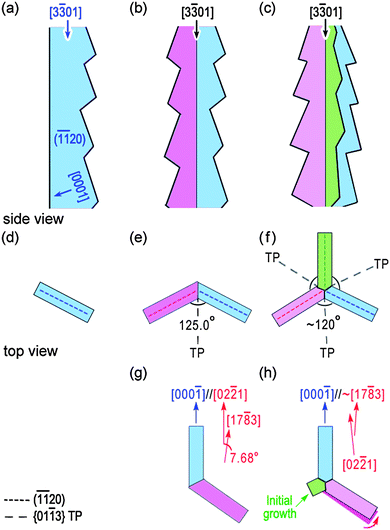
Then the intrinsic connections between bi- and tri-crystal nanobelts can simply be derived from the difference in their crystallographic relations. For a better presentation, we summarize the characteristic relationships and difference in the schematic illustrations (Fig. 9) and make a discussion where Fig. 9a to c are under side view mode, the rest are under top view mode.
 | ||
| Fig. 9 Schematic illustrations of (a) single nanobelt, (b) bi-crystal nanobelt and (c) tri-crystal nanobelt from side view. The rest are from top view showing the intrinsic connections between different morphologies. (d) Single nanobelt, (e) and (g) bi-crystal nanobelt with man-made rotation, (f) and (h) tri-crystal nanobelt at different growth stages. | ||
By introducing a strict (013) twinning, the bi-crystal nanobelt (Fig. 9b and e) forms from the matrix of a single nanobelt (Fig. 9a and d). The angle between variants I and II equals 125.0°. After a man-made rotation (same as the process from Fig. 6c–d for variant I), Fig. 9e transforms to Fig. 9g on which the characteristic relationship of [000]I//[021]II has been marked. Meanwhile, the [173] is 7.68° right away from the [000]I direction.
Once the nucleation of nanoblade III begins, nanoblade II is gradually depressed and finally results in the formation of the approximate parallel relationship between [173]II and [000]I axes, (10)II and (110)I planes (Fig. 9h). The angle between nanoblades I and II has also been depressed from ∼125.0° for a bi-crystal nanobelt to ∼120° in a tri-crystal nanobelt, facilitating the formation of a tri-crystal nanobelt mediated by {013} twinnings (Fig. 9f) and may apparently be described by the quadra-twin model.19 Because of the presence of the approximate parallel relationship between TP and corresponding (110) planes, a final asymmetric TP distribution should be observed.
The asymmetric TP distribution is further investigated by Kikuchi patterns as Fig. 10 to exactly describe this relation, due to the high sensitivity to crystallographic orientations. In comparison with the Kikuchi patterns taken from the bi-crystal and tri-crystal nanobelts as shown in Fig. 10a and g, the twinning relation is well maintained for a bi-crystal nanobelt (Fig. 10b and c), whereas there is a ∼0.75° deviation between TPs in tri-crystal nanobelts (Fig. 10h and i). Furthermore, the angle between [20]II and [023]I is ∼4.43° (Fig. 10e and f), which is very close to the theoretical value of 5.31° (as mentioned above), reconfirms this strict twinning relation.
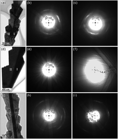 | ||
| Fig. 10 (a) BF image and corresponding Kikuchi patterns taken from (b) variant II and (c) variant I in (a) and (d) BF image and corresponding Kikuchi patterns taken from (e) variant II and (f) variant I in (d), revealing the strict twinning relationship in a bi-crystal nanobelt. (g) BF image and corresponding Kikuchi patterns taken from (h) variant II and (i) variant III, respectively, exhibiting a ∼0.75° deviation between TPs in the tri-crystal nanobelt. The dashed lines denote the center of the Laue circle. | ||
The asymmetric TP distribution has also been reflected to a certain extent from the asymmetric moiré fringes in the HRTEM images as shown in Fig. 11. The translational moiré fringe with interplanar spacing of 1.0111 nm (Fig. 11a) originates from the interference of (020)I and (01![[4 with combining macron]](https://www.rsc.org/images/entities/char_0034_0304.gif) )II planes, while the general moiré fringe with interplanar spacing of 1.9496 nm (Fig. 11c) comes from the interference of (200)I and (112)III planes with an angle of ∼4.9°. Moreover, the (10) TB is atomically sharp as shown in Fig. 11b.
)II planes, while the general moiré fringe with interplanar spacing of 1.9496 nm (Fig. 11c) comes from the interference of (200)I and (112)III planes with an angle of ∼4.9°. Moreover, the (10) TB is atomically sharp as shown in Fig. 11b.
![HRTEM images of the tri-crystal nanobelt (a) close to variant II, (b) round the twinning boundary and (c) close to variant III under [2̄5̄73̄] projection. The translational moiré fringe with dtm = 1.0111 nm originates from the interference of (2̄020)I and (011̄4̄)II planes, while the general moiré fringe with dgm = 1.9496 nm from the interference of (202̄0)I and (2̄112)III planes with angle of ∼4.9°.](/image/article/2010/CE/b914542g/b914542g-f11.gif) | ||
| Fig. 11 HRTEM images of the tri-crystal nanobelt (a) close to variant II, (b) round the twinning boundary and (c) close to variant III under [7] projection. The translational moiré fringe with dtm = 1.0111 nm originates from the interference of (020)I and (01)II planes, while the general moiré fringe with dgm = 1.9496 nm from the interference of (200)I and (112)III planes with angle of ∼4.9°. | ||
4 Conclusions
Various ZnSe nanostructures including single-, bi- and tri-crystal nanobelts have been successfully fabricated via the thermal evaporation method. Structural investigations demonstrate that all nanostructures are of metastable wurtzite structure and the bi- and tri-crystal nanobelts are both mediated by the {013} twinning, with the single nanobelts as building blocks. The crystallographic relations are fully understood by SAED, CBED and HRTEM techniques, i.e., [000]I//[021]II and (110)I//(110)II for a bi-crystal nanobelt, [000]I//∼[173]II,III and (110)I//∼(10)II,III for the tri-crystal nanobelts (aside from the coincidence of {013} TPs and the related axes in TPs). The intrinsic connections between different morphologies are fully understood revealing that accompanying the formation of tri-crystal nanobelt, the {013} relationship, maintained still, is not as strict as that in the bi-crystal nanobelt and holds a ∼0.75° deviation for a case study; the angles between adjacent twinning variants/planes are compressed from ∼125.0° in bi-crystal nanobelts to ∼120°, and finally form an asymmetric twinning plane distribution.
Acknowledgements
This work was financially supported by the Program for New Century Excellent Talents at Universities (NCET-07-0640), National Fund for Talent Training in Basic Science (Grant No. J0830310), and National University Students Training in Scientific Research Program of MOE, China (Grant No. 081048611). W.C.H. Choy thanks the University Development Fund (UDF) for support, and the seed funding from the University of Hong Kong.References
- X. D. Wang, C. J. Summers and Z. L. Wang, Nano Lett., 2004, 4, 423 CrossRef CAS.
- Y. P. Leung, W. C. H. Choy and T. I. Yuk, Chem. Phys. Lett., 2008, 457, 198 CrossRef CAS.
- R. S. Friedman, M. C. McAlpine, D. S. Ricketts, D. Ham and C. M. Lieber, Nature, 2005, 434, 1085 CrossRef CAS.
- L. J. Hall, V. R. Coluci, D. S. Galvão, M. E. Kozlov, M. Zhang, S. O. Dantas and R. H. Baughman, Science, 2008, 320, 504 CrossRef CAS.
- R. Gupta, Q. Xiong, G. D. Mahan and P. C. Eklund, Nano Lett., 2003, 3, 1745 CrossRef CAS.
- L. Lu, Y. F. Shen, X. H. Chen, L. H. Qian and K. Lu, Science, 2004, 304, 422 CrossRef CAS.
- Y. X. Chen, Q. F. Xing and S. W. Guo, Nanotechnology, 2007, 18, 245607 CrossRef.
- R. Rujkorakarn and A. J. Nelson, J. Appl. Phys., 2000, 87, 8557 CrossRef CAS.
- C. Y. Yeh, Z. W. Lu, S. Froyen and A. Zunger, Phys. Rev. B: Condens. Matter Mater. Phys., 1992, 46, 10086 CrossRef CAS.
- T. Yasuda, I. Mitsuishi and H. Kukimoto, Appl. Phys. Lett., 1988, 52, 57 CrossRef CAS.
- M. A. Haase, J. Qiu, J. M. DePuydt and H. Cheng, Appl. Phys. Lett., 1991, 59, 1272 CrossRef CAS.
- C. X. Shan, Z. Liu, X. T. Zhang, C. C. Wong and S. K. Hark, Nanotechnology, 2006, 17, 5561 CrossRef CAS.
- X. T. Zhang, K. M. Ip, Q. Li and S. K. Hark, Appl. Phys. Lett., 2005, 86, 203114 CrossRef.
- Y. P. Leung, W. C. H. Choy, I. Markov, G. K. H. Pang, H. C. Ong and T. I. Yuk, Appl. Phys. Lett., 2006, 88, 183110 CrossRef.
- L. Jin, W. C. H. Choy, Y. P. Leung, T. I. Yuk, H. C. Ong and J. B. Wang, J. Appl. Phys., 2007, 102, 044302 CrossRef.
- X. Fan, X. M. Meng, X. H. Zhang, W. S. Shi, W. J. Zhang, J. A. Zapien, C. S. Lee and S. T. Lee, Angew. Chem., Int. Ed., 2006, 45, 2568 CrossRef CAS.
- C. H. Liang, Y. Shimizu, T. Sasaki, H. Umehara and N. Koshizaki, J. Phys. Chem. B, 2004, 108, 9728 CrossRef CAS.
- S. Y. Liu, W. C. H. Choy, L. Jin, Y. P. Leung, G. P. Zheng, J. B. Wang and A. K. Soh, J. Phys. Chem. C, 2007, 111, 9055 CrossRef CAS.
- Z. Liu, X. T. Zhang and S. K. Hark, J. Phys. Chem. C, 2008, 112, 8912 CrossRef CAS.
- Z. Liu, X. T. Zhang and S. K. Hark, Cryst. Growth Des., 2009, 9, 803 CrossRef CAS.
- X. T. Zhang, K. M. Ip, Z. Liu, Y. P. Leung, Q. Li and S. K. Hark, Appl. Phys. Lett., 2004, 84, 2641 CrossRef CAS.
- Y. Q. Wang, U. Philipose, H. Ruda and K. L. Kavanagh, J. Mater. Sci.: Mater. Electron., 2006, 17, 1065 CrossRef CAS.
- R. S. Wagner and W. C. Ellis, Appl. Phys. Lett., 1964, 4, 89 CAS.
- Y. Jiang, X. M. Meng, W. C. Yiu, J. Liu, J. X. Ding, C. S. Lee and S. T. Lee, J. Phys. Chem. B, 2004, 108, 2784 CrossRef CAS.
- Z. L. Wang, X. Y. Kong and J. M. Zuo, Phys. Rev. Lett., 2003, 91, 185502 CrossRef CAS.
- C. Ma, D. Moore, J. Li and Z. L. Wang, Adv. Mater., 2003, 15, 228 CrossRef CAS.
- R. Egerton, Electron energy-loss spectroscopy in the electron microscope, 2nd edn, Plenum Press, New York, 1996, p. 302 Search PubMed.
- This angle strongly depends on the c/a ratio for a real crystal.
- S. Takeuchi, H. Iwanaga and M. Fujii, Philos. Mag., 1994, 69, 1125 Search PubMed.
- J. Q. Hu, Y. Bando and D. Golberg, Small, 2005, 1, 99 CrossRef CAS.
- J. F. Gong, S. G. Yang, H. B. Huang, J. H. Duan, H. W. Liu, X. N. Zhao, R. Zhang and Y. W. Du, Small, 2006, 2, 732 CrossRef CAS.
- F. Cao, Q. Y. Lu, S. H. Xie and D. Y. Zhao, Adv. Mater., 2002, 14, 1537 CrossRef CAS.
- W. Nie, J. B. He, N. N. Zhao and X. L. Ji, Nanotechnology, 2006, 17, 1146 CrossRef CAS.
- M. Shiojiri and C. Kaito, J. Cryst. Growth, 1981, 52, 173 CrossRef CAS.
- M. Nespolo and G. Ferraris, Eur. J. Mineral., 2004, 16, 401 CrossRef CAS.
- A. Béré and A. Serra, Phys. Rev. B: Condens. Matter Mater. Phys., 2003, 68, 33305 CrossRef.
Footnote |
| † Electronic supplementary information (ESI) available: HRTEM images of a single nanobelt (Fig. S1); tri-crystal nanobelt which can be simply regarded as a bi-crystal base (i.e., I and II) plus the third nanoblade (i.e., III) has a length of several micrometers (Fig. S2); the products can be etched with a long time immersion in the alcohol (chemically pure) and leave the relics (Fig. S3). See DOI: 10.1039/b914542g |
| This journal is © The Royal Society of Chemistry 2010 |