
 Open Access Article
 This Open Access Article is licensed under a Creative Commons Attribution-Non Commercial 3.0 Unported Licence
Regulating buried interface properties and alleviating micro-strain of crystals for efficient perovskite solar cells†
Shendong
Xu‡
a,
Guozhen
Liu‡
 *ab,
Haiying
Zheng
c,
Yuli
Tao
a,
Hui
Zhang
ac,
Liying
Zhang
a,
Liangzheng
Zhu
a,
Jiajiu
Ye
a,
Jinfeng
Li
*d and
Xu
Pan
a
*ab,
Haiying
Zheng
c,
Yuli
Tao
a,
Hui
Zhang
ac,
Liying
Zhang
a,
Liangzheng
Zhu
a,
Jiajiu
Ye
a,
Jinfeng
Li
*d and
Xu
Pan
a
aKey Laboratory of Photovoltaic and Energy Conservation Materials, Institute of Solid State Physics, Hefei Institutes of Physical Science, Chinese Academy of Sciences, Hefei 230031, P. R. China. E-mail: gzliu@issp.ac.cn
bState Key Laboratory of Fine Chemicals, School of Chemistry, Dalian University of Technology, Dalian 116024, P. R. China
cInstitutes of Physical Science and Information Technology, Anhui University, Hefei 230601, P. R. China
dInstitute of Systems Engineering, Chinese People's Liberation Army Academy of Military Sciences, Beijing 100141, P. R. China
First published on 20th July 2023
Abstract
Surface properties of SnO2 and their effects on the growth of perovskite films play a crucial role for perovskite solar cells (PSCs). Herein, a facile strategy to synchronously regulate the buried interface defects and energy level arrangement, as well as improve the crystallinity of perovskite films with alleviated micro-strain by pre-modifying the SnO2 surface with ammonium hexafluorophosphate (NH4PF6) is proposed. The device achieved the promising PCE of 22.50% and improved stability.
Perovskite solar cells (PSCs) have emerged as one of the most promising candidates for next-generation photovoltaic technologies in terms of outstanding photoelectric performance and low temperature fabrication process.1–4 In the typical n–i–p PSCs, because the buried interface is not easy to observe and characterize, the regulation of the buried interface formed between the perovskite film and the electron transport layer (ETL) is still insufficient.5,6 In particular, the modification of the buried interface is vital for the improvement of carrier extraction and the suppression of non-radiative recombination losses in the PSCs.
PSCs based on the SnO2 ETL have been extensively studied and made unprecedented progress, which is mainly due to the excellent optoelectronic properties and the advantages of low-temperature processing.7 Generally, there are a large number of oxygen vacancies and hydroxyl group defects on the surface of SnO2 films, leading to severe charge recombination.8,9 The energy level barrier between SnO2 and perovskite is also a key factor that hinders electron extraction and performance improvement.10–13 Chen and co-workers employed the multifunctional chemical linker 4-imidazoleacetic acid hydrochloride (ImAcHCl) to realize defect passivation and regulate energy level alignment.12 In addition, the SnO2 not only serves as the ETL but also provides support for the crystallization growth of the perovskite film. This means that the surface properties (hydrophilicity, roughness, etc.) will have an additional effect on the nucleation crystallization process and then affect the film quality.9,14 The interface modification strategy with residual strain and micro-strain release effect can also improve the photovoltaic performance of devices.15,16 Therefore, regulating the properties of the buried interface is more challenging compared with that of the top surfaces of perovskite films.
In this work, we realized a multi-effect strategy by using ammonium hexafluorophosphate (NH4PF6) as the modifier for the SnO2/perovskite buried interfaces. We find that pre-treated SnO2 surface displayed eliminated oxygen vacancies and hydroxyl groups and alleviated energy mismatch. According to the density functional theory (DFT) calculations, we argue that the PF6− fluorine-rich pseudo-halide anion can compensate the halide anion vacancies and suppress the formation of organic cation vacancies via hydrogen bond or electrostatic interaction formation, leading to reduced defect density and better crystallization growth of the perovskite. Moreover, the GIXRD analysis suggests that the synergistic effect of NH4PF6 can remarkably release the residual strain of the perovskite film.
To understand the chemical interaction between ammonium hexafluorophosphate (AHFP) and SnO2, X-ray photoelectron spectroscopy (XPS) characterization of the control and the AHFP-treated SnO2 films was performed. As shown in Fig. 1(a), the binding energy of the Sn 3d5/2 (486.5 eV) and Sn 3d3/2 (495.7 eV) peaks for the AHFP-treated SnO2 film shifted about 0.7 eV toward higher binding energy, which is mainly owing to the strong electrostatic coupling interaction between PF6− with high electronegativity in AHFP and Sn4+ in SnO2.11,13 It is also possible that AHFP may inhibit the formation of oxygen vacancies and thus the average chemical valence state of the Sn element was increased.10,15 From the O 1s spectra in Fig. 1(b) and (c), the peak that appeared at 530.5 eV for the control SnO2 was attributed to the lattice oxygen in SnO2 and the other peak at 531.2 eV was assigned to the oxygen vacancies or surface absorbed hydroxyl groups.13 The amount of oxygen vacancies or surface absorbed hydroxyl groups for the AHFP-treated SnO2 film went down from 66.65% (control film) to 28.38%, which may attribute to the formation of the coordinate bond between F and SnO2.11 In addition, it can be seen from Fig. S3 (ESI†) that the conductivity of the AHFP-treated SnO2 film was significantly improved, indicating that the pre-treated SnO2 interface will provide more effective charge transfer and a good promotion effect on improving the device performance.
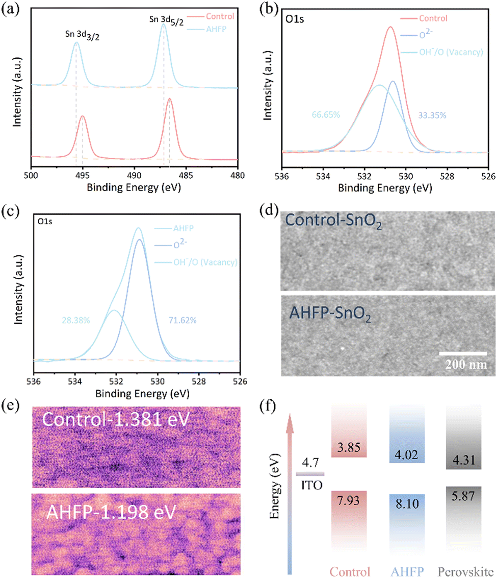 | ||
| Fig. 1 XPS spectra of the control and AHFP-treated SnO2 films for (a) Sn 3d and XPS spectra of O 1s for pristine SnO2 (b) and SnO2 with AHFP (c). (d) Top-view SEM images and (e) Kelvin probe force microscopy (KPFM) images of the control and AHFP-treated SnO2 films. (f) Energy band diagram for the control, AHFP-treated SnO2 ETLs and perovskite. | ||
Fig. 1(d) compares the top view SEM images of SnO2 and AHFP-treated SnO2 films, the AHFP-treated SnO2 film displayed a good surface morphology without pinholes. To further probe the influence of the AHFP on the surface energy levels of the SnO2, Kelvin probe force microscopy (KPFM) and ultraviolet photoelectron spectroscopy (UPS) measurements were conducted. As shown in Fig. 1(e), the AHFP-treated film revealed a lower (200 mV) surface potential than that of the control film, which indicates that the work function of the AHFP-treated SnO2 film increased by about 0.2 eV. As illustrated in Fig. S4 (ESI†), the Fermi levels (EF) of the control (4.3 eV) and AHFP-treated (4.5 eV) SnO2 films were calculated by the equation EF= hν − Ecut-off (hν = 21.22 eV), which is consistent with the results of KPFM. The valence band maxima (VBM) were further calculated to be 7.93 and 8.1 eV by the equation of VBM = EF + Eon-set. In addition, the conduction band minimum (CBM) of the SnO2 was calculated by the VBM and the bandgap values (Fig. S5, ESI†). Fig. 1(f) shows the energy level diagram of control-SnO2/AHFP-SnO2/perovskite in this work. The reduced CBM level of AHFP-treated SnO2 is closer to that of the perovskite, which is beneficial for reducing the energy loss, improving charge extraction and suppressing nonradiative recombination losses, yielding a higher photovoltaic performance for PSCs.15
As shown in Fig. 2(a) and (d), contact angle tests were conducted on the control and AHFP-treated SnO2 films. Possibly due to the hydrophilicity of the ammonium cation, the wettability of the SnO2 treated with AHFP was obviously enhanced with lower contact angle values (20.12°). Good wettability will reduce the Gibbs free energy of heterogeneous nucleation and bring about low interfacial energy, promoting to nucleation process and uniform distribution (Fig. 2(b) and (e)).9Fig. 2(c) and (f) show the top-view SEM images of perovskite films grown on the control and AHFP-treated SnO2 substrates. It is not difficult to observe that the perovskite grown on the AHFP-treated SnO2 substrate presented a significant increase in grain size. Meanwhile, according to the embedded images, the perovskite film with large grains possessed stronger hydrophobicity, which is mainly due to the reduction of the grain boundaries. Fig. S6 (ESI†) further shows the cross-section SEM image of the perovskite films. It can be observed that the grain size of the perovskite film grown on the AHFP-treated SnO2 substrate is larger and penetrates through the whole film.
 | ||
| Fig. 2 Contact angles of the water and schematic diagram of the perovskite nucleation processes on the (a) and (b) control and (d) and (e) AHFP-treated SnO2 films. (c) and (f) Top-view SEM images of the perovskite films on the control and AHFP-treated SnO2 films. | ||
Besides, X-ray diffraction (XRD) patterns and UV-vis absorption spectra were carried out to examine the crystallization of perovskite films based on different ETL substrates. As shown in Fig. S7 (ESI†), the film based on AHFP-treated SnO2 displayed enhanced peak intensity and smaller full width at half maximum (FWHM). In Fig. S8 (ESI†), the film based on AHFP-treated SnO2 displayed stronger absorption properties.
The influence of residual strain (stress) in perovskite thin films on the final device performance has attracted much attention, and is also an important parameter reflecting the crystal quality of perovskite films.15 Therefore, the effect of bottom-interface modification on the residual strain of the perovskite film was studied by depth-dependent grazing incident X-ray diffraction (GIXRD). We chose to regulate the incident angle (ω = 0.3°, 0.5°, 0.7°, 0.9°, 1.1°, 1.3°, 1.5°) to analyze the strain conditions at different depths. High diffraction angle can reflect the internal structure information of the crystal more reliably. The diffraction peak corresponding to the (211) crystal plane was chosen for further analysis. As shown in Fig. 3(a) and (b), the diffraction peak of the perovskite film grown on the control SnO2 substrate gradually moved in the lower angle direction with the increase of the incident angle (ω), while the movement degree for the perovskite film on the AHFP-treated substrate was effectively alleviated. According to Bragg's formula, as the diffraction peak position shifts in the lower angle direction, the corresponding crystal plane spacing becomes larger, resulting in lattice expansion, which is mainly caused by lattice defects and heating annealing. The calculation results of the crystal plane spacing are shown in Fig. 3(c). We speculated that the main mechanism of AHFP alleviating the residual strain of the perovskite film is that the PF6− ion in AHFP can compensate the halogen vacancies near the bottom-surface of the perovskite film and interact with the uncoordinated Pb2+ ion at the same time, which can inhibit the lattice deformation of the perovskite while rivet perovskite and SnO2. Fig. 3(d)–(f) shows the process of PF6− ion compensating halogen vacancies to relieve lattice strain.
 | ||
| Fig. 3 GIXRD spectra of the perovskite film deposited on (a) control and (b) AHFP-treated SnO2 substrates at different grazing incidence angles. (c) d-spacing value of the (211) plane as a function of grazing incidence angle for the perovskite film on the control and AHFP-treated SnO2 substrates. (d)–(f) Schematic diagram of the mechanism for relieving residual strain of the perovskite film. (g) Theoretical models of the perovskite with surface passivation of the halide ion vacancy with PF6−. (h) Defect formation energies in the perovskite films on control and AHFP-treated SnO2 substrates. | ||
In order to further understand whether the PF6− ion adsorbing on the surface of the perovskite will have an impact on the formation of surface defects (Pb vacancy VPb, I vacancy VI, and Pb–I antisite PbI), the defect formation energies (DFEs) of the perovskite with AHFP were calculated through the density functional theory (DFT) method (Fig. 3(g) and Fig. S9, ESI†). As shown in Fig. 3(h), when one halogen atom was replaced by a PF6− ion, the DFEs of different surface defects presented a slight increase. It can be predicted that when a large number of PF6− ions are adsorbed on the surface of the perovskite, the DFEs will be greatly increased, thus reducing the surface defect density and stabilizing the crystal structure of the perovskite.
As shown in Fig. S10 (ESI†), the steady-state PL quenching effect of the AHFP-treated film was significantly stronger than that of the control film, indicating that the AHFP-treated interface can promote charge extraction between SnO2 and perovskite.17 Then, we employed the space charge limited current (SCLC) method to study the defect density in the devices in Fig. 4(a). It showed ohmic characteristics at low voltage. As the voltage increases, the internal part of the device gradually enters the defect filling process, and the critical voltage between the ohmic region and the defect filling region is defined as the trap-filling limit voltage (VTFL).9 According to the calculation of nt = (2εε0VTFL)/(eL2), the defect density of the AHFP-treated device was reduced from 1.61 × 1015 cm−3 (control) to 7.74 × 1014 cm−3. Moreover, from the Vocversus light intensity (V–L) measurement in Fig. 4(b), the slope of the V–L in the AHFP-treated device is 1.07KT/q, which is 1.28KT/q in the control device, indicating that the trap-assisted non-radiative recombination in the AHFP-treated device was significantly inhibited.13 Electrochemical impedance spectroscopy (EIS) was used to investigate the interface transmission and recombination characteristics in the devices. As shown in Fig. S11 (ESI†), the circuit model conforming to PSCs was adopted and the final fitting data are shown in Table S1 (ESI†).
 | ||
| Fig. 4 (a) Dark I–V curve of the electron-only devices (ITO/SnO2/perovskite/PCBM/Au) with control or AHFP-treated SnO2 ETL. (b) Vocversus light intensity plots of devices with control or AHFP-treated SnO2 ETL. (c) J–V curves of the devices with control or AHFP-treated SnO2 ETL. (d) The long-term stability test (unencapsulated PSCs) under an air atmosphere in the dark of the devices with control or AHFP-treated SnO2 ETLs. | ||
The PSCs were fabricated in a planar architecture (Fig. S12, ESI†). As shown in the J–V curves (Fig. S13, ESI†), it was found that the optimal performance of the devices at the interface between SnO2 and perovskite was demonstrated by the improvement of the open circuit voltage (Voc) and short circuit current (Jsc) when the concentration of AHFP was 0.2 mg mL−1. As shown in Fig. 4(c), the J–V curves were tested under a standard AM1.5G illumination. The PCE of the AHFP-treated device increased from 20.76% (control) to 22.50%, and the corresponding Voc, Jsc and FF increased from 1.15 to 1.17 V, from 23.90 to 24.62 mA cm−2, and from 75.79% to 77.78%, respectively. Fig. S14 (ESI†) presents the reverse and forward J–V curves of different devices. The hysteresis suppression of the AHFP-treated device may be attributed to the alleviated charge accumulation at the interface and the inhibited ion migration.11 The incident photon-to-electron conversion efficiency (IPCE) spectra of the corresponding devices are presented in Fig. S15 (ESI†). In the whole wavelength range, the IPCE of the AHFP-treated device is slightly higher than that of the control device. In Fig. S16 (ESI†), the AHFP-treated device displayed a steady current density of 21.20 mA cm−2 and PCE of 21.20%. Fig. S17–S20 (ESI†) shows the statistical diagram of the photovoltaic parameters based on several devices. In Fig. 4(d), the AHFP-treated device could still maintain about 90% of the initial PCE after 2000 hours in the environment, while the PCE of the control device decline to 85% of the initial value. This may be attributed to the release of lattice strain, which can inhibit the occurrence of stress-induced decomposition reaction. In addition, as the defects in unencapsulated devices can become the site of erosion, the reduced defect density can also enhance the stability of devices.
In conclusion, we have explored a strategy for regulating the buried interface and alleviating the micro-strain of crystal in PSCs. The results show that the pre-treated NH4PF6 can not only improve the electron extraction and reduce the defect density at the interface, but also promote the formation of large grains and high-quality perovskite films. Based on DFT calculation, we find that the PF6− can increase the DFEs by forming strong ionic bonds with Pb2+ and strong hydrogen bonds with organic cations (MA/FA) at the bottom interface. As a result, the device treated by NH4PF6 achieved an enhanced performance with a champion PCE of 22.50% and good long-term stability under environmental conditions. These findings provide a simple and effective strategy to regulate the buried interface in n–i–p PSCs.
The authors would like to thank the National Natural Science Foundation of China (U22A20142, 52272252) and the Natural Science Foundation of Anhui Province (Grant 2108085J34) for the financial support.
Conflicts of interest
There are no conflicts to declare.Notes and references
- A. Younis, C.-H. Lin, X. Guan, S. Shahrokhi, C.-Y. Huang, Y. Wang, T. He, S. Singh, L. Hu, J. R. D. Retamal, J.-H. He and T. Wu, Adv. Mater., 2021, 33, 2005000 CrossRef CAS PubMed
.
- L. Song, Mater. Rep.: Energy, 2022, 2, 100171 Search PubMed
- H. Xiang, P. Liu, R. Ran, W. Wang, W. Zhou and Z. Shao, Renewable Sustainable Energy Rev., 2022, 166, 112614 CrossRef CAS
- NREL, Best research-cell efficiency chart, 2023. https://www.nrel.gov/pv/cell-efficiency.html.
- W. Shen, Y. Dong, F. Huang, Y.-B. Cheng and J. Zhong, Mater. Rep.: Energy, 2021, 1, 100060 CAS
- Z.-W. Gao, Y. Wang and W. C. H. Choy, Adv. Energy Mater., 2022, 12, 2104030 CrossRef CAS
- C. Altinkaya, E. Aydin, E. Ugur, F. H. Isikgor, A. S. Subbiah, M. D. Bastiani, J. Liu, A. Babayigit, T. G. Allen, F. Laquai, A. Yildiz and S. D. Wolf, Adv. Mater., 2021, 33, 2005504 CrossRef CAS PubMed
- E. H. Jung, B. Chen, K. Bertens, M. Vafaie, S. Teale, A. Proppe, Y. Hou, T. Zhu, C. Zheng and E. H. Sargent, ACS Energy Lett., 2020, 5, 2796–2801 CrossRef CAS
- Y. Dong, W. Shen, W. Dong, C. Bai, J. Zhao, Y. Zhou, F. Huang, Y.-B. Cheng and J. Zhong, Adv. Energy Mater., 2022, 12, 2200417 CrossRef CAS
- B. Zhang, J. Oh, Z. Sun, Y. Cho, S. Jeong, X. Chen, K. Sun, F. Li, C. Yang and S. Chen, ACS Energy Lett., 2023, 8, 1848–1856 CrossRef CAS
- H. Bi, B. Liu, D. He, L. Bai, W. Wang, Z. Zang and J. Chen, Chem. Eng. J., 2021, 418, 129375 CrossRef CAS
- J. Chen, X. Zhao, S.-G. Kim and N.-G. Park, Adv. Mater., 2019, 31, 1902902 CrossRef PubMed
- Z. Xiong, X. Chen, B. Zhang, G. O. Odunmbaku, Z. Ou, B. Guo, K. Yang, Z. Kan, S. Lu, S. Chen, N. A. N. Ouedraogo, Y. Cho, C. Yang, J. Chen and K. Sun, Adv. Mater., 2022, 34, 2106118 CrossRef CAS PubMed
- P. Wang, B. Chen, R. Li, S. Wang, N. Ren, Y. Li, S. Mazumdar, B. Shi, Y. Zhao and X. Zhang, ACS Energy Lett., 2021, 6, 2121 CrossRef CAS
- Z. Zheng, F. Li, J. Gong, Y. Ma, J. Gu, X. Liu, S. Chen and M. Liu, Adv. Mater., 2022, 34, 2109879 CrossRef CAS PubMed
- Y. Zhao, H. Xiang, R. Ran, W. Zhou, W. Wang and Z. Shao, J. Energy Chem., 2023, 83, 189–208 CrossRef CAS
- C. Liu, Y.-B. Cheng and Z. Ge, Chem. Soc. Rev., 2020, 49, 1653 RSC
Footnotes |
| † Electronic supplementary information (ESI) available. See DOI: https://doi.org/10.1039/d3cc02709k |
| ‡ These authors contributed equally to this work. |
| This journal is © The Royal Society of Chemistry 2023 |