Interactions between metals and carbon nanotubes: at the interface between old and new materials
Florian
Banhart
*
Institut de Physique et Chimie des Matériaux, UMR 7504, Université de Strasbourg, 23 rue du Loess, 67034, Strasbourg, France. E-mail: Banhart@ipcms.u-strasbg.fr
First published on 28th August 2009
Abstract
The article reviews the interaction between crystalline metals and carbon nanotubes in nanocomposite systems. Starting with an introduction to the chemical interaction between metal atoms and graphitic layers, an overview of the fields of nanotechnology is given where metal–carbon interaction comes into play. The interface between metals and carbon nanotubes is of interest in junctions between nanotubes and their periphery, for example in metallic contacts for electronic devices or in metal supports for carbon nanotube components. Furthermore, metals determine the catalytic growth of carbon nanotubes. The behaviour of individual metal atoms in or on carbon nanotubes is treated as well as the interaction between crystalline metals and nanotube surfaces. Emphasis is put on the common mechanisms of metal–carbon interaction that play a role in such different fields as the electrical transport through a metal–nanotube contact or the catalytic growth of nanotubes from metal particles.
 Florian Banhart Florian Banhart | Florian Banhart received his PhD in physics from the University of Stuttgart (Germany) in 1988. From 1989 to 1999 he was a research scientist at the Max Planck Institute for Metals Research in Stuttgart and from 1999 to 2003 at the University of Ulm. He joined the University of Mainz as a professor of Physical Chemistry in 2003 and the University of Strasbourg (France) in 2007 as a professor of Physics. His main research activities are in the fields of electron microscopy, irradiation effects, and nanostructures of carbon and other materials. |
Introduction
Whereas metals are among the first materials to have been used by mankind, carbon nanotubes were discovered only two decades ago and are just finding their way to their first applications in industrial products. The physical properties of carbon nanotubes1–4 are, in view of their applicability, in many respects superior to the properties of metals. Hopes have been raised that nanotubes could initiate a technological revolution and pave the way towards technologies such as nanoelectronics within a short time. These expectations were exaggerated, as we know today, and this is mainly due to unexpected difficulties in the large-scale synthesis of carbon nanotubes with uniform structure and properties.Planar graphene is an alternative material, but closely related to carbon nanotubes, and was synthesized a few years ago.5 It has been suggested that graphene could be even superior to carbon nanotubes in several applications, e.g., nanoelectronics. However, the difficulties of synthesizing single-layer graphene on a large scale or graphene nanoribbons with atomically smooth edges haven't been overcome either (although these problems are different from those encountered in carbon nanotube synthesis), and the application of carbon nanotubes as well as graphene still depends on advances in the production of high-quality material on a large scale. Nevertheless, the huge amount of research devoted to the advancement of graphitic materials such as carbon nanotubes or graphene is certainly justified. Before monocrystalline silicon, as an example, could become available in purity and perfection and, last not least, at low cost for today's microelectronic mass products, decades of intense research were necessary.
Carbon nanotubes as well as graphene have shown remarkable properties.1–4 These are mainly due to the high perfection of the graphenic lattice and the absence of impurities or crystallographic defects. Their enormous mechanical strength is based on the strong σ-bond between carbon atoms in the layers, whereas the electronic properties6 (e.g., semiconducting or metallic behaviour or ballistic conductance) are determined by the overlap between the π-bonds that extend normal to the layers and are responsible for charge transport.
Many properties of carbon nanotubes have been predicted theoretically and were later confirmed by numerous experiments. It is instructive to see how systems such as carbon nanotubes are both small enough to be treated by atomistic computer simulations and large enough for an experimental characterization of individual objects. Thus, the number of studies treating exactly the same systems by both theory and experiment increases, and a complete understanding of the properties of these systems has in many cases been achieved.
It is hard to imagine that isolated graphenic nanosystems (consisting of carbon only) could build up any useful system. Metals are indispensable in the synthesis of carbon nanotubes and as a link between carbon nanotubes and their periphery. It is therefore impossible to investigate or apply carbon nanotubes without implying metals from where the carbon nanotubes grow and to where they are attached to link them with their environment. The combination of metal and graphitic carbon could be one of the most important material systems in future nanotechnology. For applications in ultrastrong mechanical components, carbon nanotubes have to be attached to a support, preferably to a metal. In carbon nanotube electronics,7–9 contacts have to be established to create heterojunctions in semiconducting devices or just a link to conventional metal contacts. Creating connections with well-defined properties between graphitic structures and non-carbon materials such as metals is a challenging field in modern nanotechnology.
Metals play another important role in carbon nanotube technology. The nucleation and growth of carbon nanotubes, in particular of single-wall species, relies on the application of metallic catalysts. The interaction between metals of different types and carbon atoms is a highly important issue in the growth of carbon nanotubes or graphene layers. Without detailed knowledge of the processes occurring at the interface between graphitic carbon and a metal crystal, the reliable production of carbon nanotubes with pre-defined and uniform structure cannot be expected.
An overview of the interactions between metal crystals as ‘conventional materials’ and carbon nanotubes as ‘new materials’ is given in this review. A large variety of studies on metal–graphite nanosystems has already been undertaken in the past decade,10 and quite unexpected phenomena occurring in these nanocomposites have been observed. Of particular importance is the interface between a graphitic system and a metal crystal. Due to the anisotropy of the graphitic lattice, different types of interfaces with completely different properties are possible.
The interaction between metals and graphitic structures is a wide field, and a comprehensive review cannot be given here. The present overview tries to address the most important aspects and applications of the interaction between carbon nanotubes and metals, but without going into the details of each application. Since extensive reviews of different aspects, e.g., carbon nanotube electronics and electrical contacts6,8,11 or carbon nanotube growth from metals2–4,12 have recently been published, the present article aims at relating the different fields to each other. Due to the novelty of planar graphene and the lack of detailed studies of metal–graphene connections, graphene will not be treated in detail here. Nevertheless, the physics and chemistry at the interface between carbon nanotubes and metal crystals is closely related to the metal–graphene interface and can be treated exemplarily.
Structure and bonding at the metal–carbon interface
Carbon nanotubes (CNTs) are built up of either a cylindrically closed sheet of graphene, constituting a single-wall nanotube (SWNT), or a multi-wall nanotube (MWNT) consisting of several nested graphenic cylinders. The crystallography of CNTs is therefore based on the structure of graphene or graphite. A characteristic feature of graphite is the extreme anisotropy of the structure and almost all physical properties.13 The carbon atoms in graphitic structures are sp2-hybridized and held together by strong covalent σ-bonds within a basal plane. At the edge of the plane, covalent bonds can be formed with other atom species, e.g., hydrogen atoms (that usually saturate the dangling carbon bonds) or to metal atoms. The π-orbitals of carbon extend normal to the basal plane and allow only weak bonding to neighbouring graphenic basal planes or to other materials in contact with the plane. Metal crystals, on the other hand, do not have the anisotropy of graphite and form similar bonds in all three dimensions of space.Due to the anisotropy of graphite, two completely different interfaces between a graphitic system such as a CNT and a metal crystal exist as shown in Fig. 1. The CNT may constitute an end-contact to the metal, involving covalent bonds at the interface, or a side-contact where the metal forms a weakly bonded interface with the outer or inner surface of the tube. Until now, much more experimental work has been devoted to the side-contact interface. This has technical reasons and is due to the way of making electrical contacts to CNTs (that are usually lying on a substrate) by depositing a metal strip from above. Due to the stronger bonding and the better coupling at the interface, an end-contact should be favourable, at least when a mechanically resistant link between a CNT and a metal support is desired. Nevertheless, side contacts with excellent electrical properties have already been made. The end-contact is of particular importance in the catalytic growth of CNTs that occurs in such a way that a CNT sprouts from a metal particle with the CNT axis normal to the metal surface.
 | ||
| Fig. 1 The two types of interface between a metal crystal and a carbon nanotube: end-contact (top) and side-contact (bottom).14 (Courtesy of J. J. Palacios, reprinted with permission from the American Physical Society). | ||
Transition metals are of special interest in metal–CNT systems due to their electronic structure. The bonding between metal and carbon increases with the number of unfilled d-orbitals in the metal. The hybridization for a side-contact15 is determined by the overlap of the pz-orbitals of carbon (normal to the surface of CNTs) and the d-orbitals of transition metals. End-contacts are established by saturating a dangling bond in the graphenic plane (that would otherwise form a σ-bond with another carbon atom) with a d-electron from the transition metal atom. Au or Pd have no unfilled d-orbitals and therefore a low affinity for carbon. Metals with a few vacant d-orbitals (Ni, Fe, Co) have a higher affinity which is also reflected by the fact that these metals have a certain (yet low) solubility for carbon. Metals of 3d- and 4d-type with vacant d-orbitals (Ti, Nb) form strong bonds with carbon. Strong metal–carbon bonds can lead to a quantitative solid-state reaction and to the formation of stable carbides. Junctions between SWNTs and carbide crystals have already been made by solid-state reactions.16
Junctions between metals and carbon nanotubes
End-contact junctions
The existence of a stable end-contact, where the end of a CNT forms a covalently bonded interface with a metal crystal, has already been demonstrated experimentally. Junctions between MWNTs and metals or semiconductors have been made, e.g., by the catalytic growth of MWNTs on Si nanowires,17 by a combination of CVD and electrodeposition,18 by passing an electrical current through a metal–CNT contact,19,20 or by electron irradiation of metal–nanotube composites.21 In CVD-grown metal-filled MWNTs, junctions between metal crystals and MWNTs can also be found occasionally. An example of an interface between a FeCo crystal and a MWNT as obtained from a CVD process is shown in Fig. 2. | ||
| Fig. 2 End-contact junction between a FeCo (alloy) crystal and a MWNT as obtained from CVD synthesis of CNTs in the presence of metallocenes. (STEM image by J. A. Rodriguez-Manzo). | ||
Indications for the covalent nature of the bonds have been found experimentally by large mismatch-induced strains at the interface21 or by the high tensile strength of such a junction.22 The theoretical treatment shows a surprisingly high binding energy of, e.g., 7.6 eV for a single bond at a SWNT–Co interface.21 Density functional calculations confirm covalent bonds across the interface. The delocalization of charge across the interface leads to a metallic (Ohmic) character (in contrast to the tunnelling that would be expected for van der Waals bonding). As a model system for this type of metal–carbon bonding, the interaction between metal crystals and benzyl radicals has been studied theoretically.23 A decreasing interaction from left to right in the periodic table (less filled to filled d-orbitals) has been found.
The end-contact of a SWNT to a metal is already established during growth of the tube from a catalytically active metal crystal. Fig. 3 shows an experimental image where a SWNT grew between two Co tips in an in situelectron microscopy experiment.24 The inset shows the structure of a contact between a (9,0)-SWNT and a (111)-Co surface.
 | ||
| Fig. 3 End-contacts between a SWNT and Co crystals. A SWNT bridges the gap between two Co cones.24 The inset (Courtesy of B. Sumpter and V. Meunier) shows the structure of a SWNT–metal interface for the example of a (9,0) tube on a (111) surface of Co. | ||
Side-contact junctions
Due to the weak bonding, the side-contact interface between a graphitic layer and a metal is determined by surface wetting.25 The (0001) surface of graphite is chemically rather inert. It is assumed that weakly bonded metals are attached to the graphite surface by van der Waals bonding, and covalent chemical bonds are absent. However, a re-hybridization sp2 → sp3 of carbon atoms within the tubes occurs locally when the adhesion of the metal is strong. This may lead to the formation of covalent side-bonds to metal atoms which goes along with a deformation of the CNT.25It has been shown that the nature of the contact depends on the type of metal.26,27 Good wetting (Ti, Ni, Pd) allows deposition of continuous metal layers on CNTs whereas poor wetting (Al, Fe, Au) leads to isolated metal islands. However, wetting also depends on the internal binding energy of the metal so that the balance between the bond energies (metal–carbon and metal–metal) determines the formation of a metal layer. Furthermore, small metal clusters of some elements are inherently unstable, leading to better wetting of the graphitic surface. In the case of low wetting, the mobility of atoms or small clusters on the graphene surface is high, inducing the coalescence of particles and Ostwald ripening.
The binding energy between a metal atom and a graphitic surface determines which metal sticks best to the surface, but is not conclusive of the electrical properties of the contact.25 For example, Ti has a higher cohesion energy on the surface than Pd and therefore a better wetting, but Ti forms a poorer (mostly non-Ohmic) electrical contact. Fig. 4 shows an example of the calculated charge density at the interface between Pd or Ti atoms and a graphene surface. In the case of Pd, excess charge accumulates between the Pd atom and the graphene layer whereas charge accumulation is seen in the atomic layers for the Ti/graphene system where the interlayer region is depopulated.15
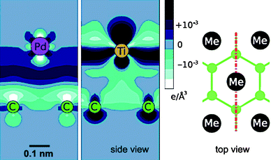 | ||
| Fig. 4 Calculated charge-density distribution at the interface between monolayers of Pd (left image) and Ti (middle image) and a graphene layer.15 The image on the right hand side shows a top-view of the geometry. The red line indicates the cross-section in the charge density maps. (Courtesy of D. Tománek, reprinted with permission from the American Physical Society). | ||
The interface between the surface of CNTs and metals has been studied in detail.26 The interface energy depends on the curvature of the graphitic layer. Isolated pz-orbitals (low overlap with neighbouring orbitals) have a higher reactivity than strongly overlapping orbitals. The outer (convex) surface of a CNT therefore has a different electronic structure and a higher reactivity than planar graphite28 or the inner surface of a tube. The interaction with metal atoms also depends on the presence of structural defects in the tubes. Even if dangling carbon bonds are absent at structural defects in the shape of non-hexagonal rings (pentagons, heptagons), the interaction with metal atoms is enhanced. This is due to the local deviation from pure sp2-hybridization. Covalent bonding with metal atoms is generally facilitated at defects in the tubes where the coherence of the surface layer is interrupted and dangling carbon bonds occur. This has been made use of in a metal decoration technique to detect defects in CNTs.29
The role of single atoms: bonding, diffusion and solubility
Bonding of metal atoms to carbon nanotubes
Metal atoms can interact with graphenic layers by adsorption on the surface (ad-atom), as treated above, or by incorporation into the layer by replacing one or several carbon atoms (substitution). Metal atoms in vacancies of CNTs or graphene are of particular interest in the context of magnetism (see the section below). For the binding energies Eb of individual metal ad-atoms to the surface of carbon nanotubes or graphite (or graphene), the sequence Ti > Ni > Pd > Fe > Al > Au has been suggested.26 Theoretical studies show that atoms of some elements prefer positions above the centre of a hexagon while other atom types prefer positions above a C atom or bridge sites over the edge of a hexagon.30 The situation on planar graphene may be different from curved CNTs,28 as mentioned above.Individual metal atoms are incorporated into the graphenic layer by replacing carbon atoms and forming covalent bonds to the neighbouring carbon atoms. Such a replacement would have a prohibitively high energy barrier and would not occur in a thermal process, but an existing single or multiple vacancy in the graphenic layer can trap a metal atom. It has been found that many transition metal atoms, even Au, form covalent bonds with undercoordinated carbon atoms around a vacancy.31 The interaction between transition metal atoms on substitutional sites and carbon atoms in the CNTs has been calculated in several studies.31,32 The trapping of metal atoms in vacancies is exothermic and has been observed, e.g., for Ni atoms in irradiation-induced vacancies of spherical graphitic layers.33 This is shown in Fig. 5 where a Ni crystal is encapsulated in a spherical multi-layer graphitic shell. Many carbon atoms in the shell have been replaced by Ni atoms under energetic electron irradiation. The substitutional Ni atoms form ordered arrangements in the shells. Locally, a carbidic phase may appear, but its structure has not been studied in detail yet. Other atom species such as Co or Au do not occupy stable positions in graphitic shells; instead they diffuse rapidly by jumping from one shell to another.34
 | ||
| Fig. 5 Incorporation of Ni atoms into spherical graphitic shells surrounding a Ni crystal. The composite structure has been generated under electron irradiation.33 | ||
The metal–carbon bond lengths (e.g., 0.18 nm for a C–Ni bond) are larger than the carbon–carbon bond lengths within the layer (0.14 nm), leading to a position of the metal atom slightly off the layer (typ. 0.1 nm). The out-of-tube position seems to be more stable than the in-tube position (both off-layer). Fig. 6 shows how a metal atom fits into a single vacancy and into a divacancy in graphene. The off-plane position of the metal atom is almost avoided when it is trapped in a divacancy.31
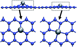 | ||
| Fig. 6 The location of a transition metal atom in a single (left) or double (right) vacancy in a graphene layer in side-view and top-view.31 (Courtesy of A. Krasheninnikov, reprinted with permission from the American Physical Society). | ||
Diffusion of metal atoms on and in nanotubes
Metal ad-atoms diffuse on a graphitic surface with a diffusivity proportional to exp(−Ea/kT) where Ea is the activation energy for migration. The interaction between the metal atom and the graphitic surface is generally weak and reflected by low binding energies and, correspondingly, rapid diffusion. Several theoretical studies for metal ad-atom adsorption and diffusion on graphene have been undertaken, giving low activation energies in the range 0.14–0.8 eV.30,31,35 Experimental measurements confirmed the low activation energies, for example 0.28 eV for Au diffusion on graphite.36 At these activation energies, metal atoms are already highly mobile at room temperature. A similar situation can be expected for the migration of metal atoms inside the inner channel of CNTs, although this has not been studied yet. At large curvature, the π-orbitals inside the innermost layer are overlapping strongly, and this could lead to an even lower affinity of the surface to metal atoms and so to an even higher mobility of the metal atoms. Thus, CNTs could act as ‘pipelines’ for the efficient transport of metal atoms.Considerably stronger bonding prevails when the metal atoms are on substitutional sites in a graphenic layer. The diffusion of a metal atom via substitutional sites requires the breaking of metal–carbon and carbon–carbon bonds and has, therefore, a higher activation energy. An experimental study revealed activation energies of 2.5 eV for the in-plane migration of both Au and Pt atoms in graphene and 2.3 eV for the migration of Pt atoms in layers of MWNTs.37Fig. 7 shows a MWNT with substitutional Au atoms in the layers, indicating a stable incorporation of Au atoms into the lattice of CNTs. This is a surprising observation in view of the weak interaction of Au with graphitic structures and indicates that the majority (if not all) transition metal atoms can be incorporated in graphene.
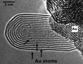 | ||
| Fig. 7 Substitutional Au atoms (arrowed) in the shells of a MWNT that is attached to a Au crystal.37 | ||
Calculations predicted activation energies for diffusion in the range 2.1–3.6 eV for metal atoms in single vacancies of graphene and values around 5 eV for metal atoms in double vacancies.31 The higher value for double vacancies is understandable with regard to the more extended reconstruction around the migrating metal atom. The diffusion of substitutional foreign atoms in graphene and CNTs is an important subject in view of the behaviour of dopant atoms and will certainly receive more attention in the future.
Carbon atoms in metals
The behaviour of carbon atoms in metals is an old subject in the science of alloys and steel and will not be considered in detail here. Nevertheless, it is of renewed interest in metal–CNT systems and gives insight into the interaction between CNTs and metals. The solubility of carbon in transition metals38,39 depends on the presence of unfilled d-orbitals; for example, metals with a few vacant d-orbitals (Ni, Fe, Co) have a finite solubility for carbon. The stability of the respective carbides decreases in the sequence Fe, Ni, Co. Of similar importance is the mobility of carbon in metals.40 A low interaction between carbon and metal and the densely packed metal lattice lead to a low solubility but a rapid diffusion of carbon via jumps between interstitial sites in the metal lattice. For example, an activation energy of 1.5 eV has been measured for carbon diffusion in fcc cobalt crystals.41The solubility of carbon atoms in transition metals is of considerable importance in the growth of CNTs from catalytically active metal particles (see below). Here the question of solubility as a function of the size of the metal particles comes into play when the sizes are in the nanometre range. A reduced solubility of carbon in small transition metal particles has recently been described.42 In another study it has been found that the enthalpy for a carbon interstitial in fcc iron increases by 0.1 eV when the diameter of the Fe particle decreases from 3 to 1.5 nm.24 This reduces the solubility by a factor of 5. Accordingly, the solubility should be influenced by the local surface curvature of the metal; under regions of high curvature the solubility for carbon atoms should be lower. The high diffusivities of carbon atoms in metals and on metal surfaces suggests that diffusion is generally not a rate-limiting process in the growth of CNTs from metals.
Mechanical properties of metal–nanotube junctions
Among all known fibre materials, CNTs have the highest strength against failure. Fracture strengths of MWNTs of more than 100 GPa have recently been measured,43 which is close to the theoretical prediction for non-defective MWNTs. First tensile measurements showed that MWNTs fail in a sword-in-sheath mechanism, where one shell slides inside the other in the axial direction.44 This is the typical situation when only the outermost shell of the tube is attached to a support. Irradiation of the MWNTs by particle beams45 leads to cross-links between the shells; the sliding of the shells can be avoided and the total strength increased.43,46 In the same way, bundles of SWNTs can be strengthened by electron irradiation, leading to cross-links between the tubes.47 The plastic deformation of CNTs under load in the axial direction has been explained by the successive formation of internal defects such as non-hexagonal rings.48 Such a rearrangement of atoms has to overcome high energy barriers and explains the high resistance of CNTs against plastic deformation.Many experiments have been carried out to measure the fracture strength, but this has been a non-trivial task because CNTs have to be attached to metal tips where they are held firmly so that the fracture does not occur at the welding point. For the first mechanical measurements, CNTs have been ‘soldered’ to a metal support by electron-beam deposition of carbon in an electron microscope.49 This resulted in a surprisingly strong contact. The nature of this contact is not well understood to date. Specimens in electron microscopes are covered with a certain amount of highly mobile hydrocarbon molecules. The hydrocarbon molecules, once arrived under the electron beam, decompose into amorphous or graphitic carbon which is immobile and forms a deposit of growing size. This has been applied at the contact region between a CNT and a metal. Presumably, it is both a side- and an end-contact to the tube that has been established in such a way, thus attaching the tube quite well with a large contact area to the metal support. The interface between the metal and an amorphous carbon deposit has not been studied in detail yet, but the large resistance against mechanical failure suggests the formation of covalent bonds at both the end and the side of the tube in such a junction.
A mechanically strong end-contact, where the end of a MWNT is covalently bonded to a metal, has been made recently by electron irradiation of a MWNT filled with a transition metal or a MWNT in outer contact with a metal particle.21,50Fig. 8 shows a measurement of the tensile strength of a junction between a MWNT and a Co contact by using an AFM tip integrated into a TEM specimen stage. The tensile strength at the point of failure is of the order 5 GPa. This is higher than the ultimate strength of steel and comparable to conventional carbon fibres. Since the electron-beam welding technique has not yet been optimized, even higher values can be expected. The measurements already show that CNTs can be attached firmly to metals. This is important in view of applications of CNTs as ultrastrong light-weight ropes. An even stronger connection could possibly be made by combining the electron-beam welding with the electron-beam deposition technique. In such a way the contact area at the metal–CNT interface can be extended to the side walls of the tube and, furthermore, links between the shells of the tubes might be created, thus again increasing the inherent strength against failure.
 | ||
| Fig. 8 Force-displacement curve for a contact between a Co crystal and a MWNT.50 (Courtesy of D. Golberg). | ||
Electronic properties of metal–CNT junctions
Charge transfer between metals and CNTs
The technological aspects of CNT implementation into devices and the techniques of attaching CNTs to contacts as well as their electrical characterization has already been subject of detailed reviews.6,8,11CNTs can be either metallic or semiconducting, depending on their structure.11,51 Whereas SWNTs of the armchair type (n = m) show metallic electron conductance, those with n − m = 3k (k is a non-zero integer) are semiconducting with a very small bandgap, and all others are semiconductors with a bandgap inversely proportional to the tube diameter.52 The electronic properties of junctions between CNTs and metals depend primarily on the metallic or semiconducting nature of the tube.It is well-established that Fermi level pinning leads to a Schottky barrier and a rectifying behaviour of the contact at the junction between a metal and a conventional semiconductor. This has indeed been found and studied in detail in various CNT–metal contacts.53–55 However, the Fermi level pinning in metal–CNT contacts is different from conventional planar contacts.56 Due to the point-like contact between a SWNT and a metal, potential shifts at the interface decay rapidly in a direction normal to the interface and disappear within a few nanometres. Therefore, the barrier (that is induced by Fermi level pinning) has a width of a few nanometres only, and electrons can tunnel through the barrier. Fermi level pinning in metal–CNT junctions is thus less important than in conventional Schottky contacts.
An Ohmic contact, on the other hand, has no rectifying behaviour and is established when the level of the metal workfunction is in the valence or conduction band of a semiconducting CNT. This is indeed the case for several metals and has been measured.57,58 Ohmic contacts are most desirable for contacting devices where the contact resistance has to be as small as possible. Fig. 9 shows schematically the energy levels for an Ohmic and a Schottky junction in the n-region and qualitatively the typical current–voltage characteristics. The Schottky junction in Fig. 9 is a conventional junction with band bending over a scale of the Debye length. At very small distances from the interface (i.e., much smaller than the Debye length), the band bending is different due to metal-induced gap states.56 Schottky and Ohmic conductance show an opposite temperature dependence. Whereas the resistivity of a Schottky contact decreases with increasing temperature, the resistivity of an Ohmic contact increases. The Schottky-type behaviour has been measured by thermal activation of a current over the barrier.59
 | ||
| Fig. 9 Energy levels for an Ohmic and a Schottky junction between a metal and a semiconductor. The current–voltage characteristics are shown schematically. | ||
The charge transfer over the junction is determined by the band bending in the contact region and by the Schottky or Ohmic characteristics. The metallicity at the junction is influenced by the action of the metal as an electron donor. A good metallicity of a junction needs a high charge density at the interface. Excess charge can be delocalized over the π-orbitals of the graphitic layer. Furthermore, a good contact needs a high density of states at the Fermi energy.
Weak bonding between the CNT and a metal contact can result in a tunnel junction or in Coulomb blockade.60 This has been observed for side-contacts when the metals were deposited on top of the CNTs,61e.g., by evaporation or sputtering. Of further interest is quantum transport at the interface of a metal–CNT junction. Quantum conductance and an anomalously large contact resistance have been found in calculations of SWNT–metal junctions.62
Side- and end-contacts
The electronic properties of contacts are mainly determined by the bonding at the interface, i.e. whether it is a side-63 or an end-contact.17 The properties of both types have been calculated and compared.14 The side-contact, as made by evaporation or sputtering of a metal, is much easier to fabricate than an end-contact and has been studied and applied in numerous CNT devices.11 Often, a large contact resistance has been measured,64 in particular when the SWNT was just lying on a metal contact without any soldering. This can lead to a tunnelling barrier with Coulomb blockade.65 However, the behaviour can be improved after the electrodeposition of a metal.66 It has also been found that coadsorbates change the contact properties.67Early studies on side-contacts between metal electrodes and MWNTs reported that the MWNTs carried current densities of more than 109 A cm−2.68Fig. 10 shows an example of such a side-contact for measuring the electrical properties of a MWNT. Experimentally and by transport calculations it has been found that an optimum metal–CNT side-contact needs a large contact area but weak hybridization at the interface.15 It is intuitively clear that a large contact area leads to a better electrical coupling. An accumulation of excess charge between the metal and the graphite surface (population of the interlayer state) appears to lead to a better carrier injection into the CNT and to a lower contact resistance. This has been found, e.g., for Pd contacts. A depopulation of the interlayer states such as for a Ti contact is less suited for charge transfer due to a high interlayer scattering potential.15 Palladium proved to be well-suited for making electrical contacts. An Ohmic side-contact has been obtained for Pd on a metallic CNT69 whereas a zero or slightly negative Schottky barrier has been measured for Pd on semiconducting CNTs.57 Field-effect transistors on the basis of SWNTs normally show a Schottky-type behaviour at the metal–SWNT contacts with a barrier of typically 0.4 eV.70 This reduces the conductance in the on-state of the transistor and thus the performance of the device. For Pd–SWNT contacts, the barrier has been eliminated, and a ballistic conductance of the SWNT has been observed.57
 | ||
| Fig. 10 AFM image of a typical contact between a MWNT and two Pt electrodes.68 (Courtesy of P. M. Ajayan, reprinted with permission from the American Institute of Physics). | ||
An end-contact has been made by different techniques, e.g., between a MWNT and Si by growth of MWNTs on Si nanowires17 or by catalytic growth of CNTs from metal particles on a TiN contact.71 The growth of the tube normal to the surface of a patterned substrate can be used to establish an end-contact. For the MWNT-Si contact, a rectifying behaviour has been observed.17 By contrast, a very low contact resistance (0.59 Ω) has been reported for a TiN contact.71 An end-contact between MWNTs or SWNTs and transition metals (Fe, Ni, Co) has recently been made by electron irradiation of CNTs where metals were either inside or on top of the CNTs.21 The contact shows Ohmic behaviour with a linear I–V curve from zero. A combination of end- and side-contacts has been made by dipping MWNTs into liquid metals such as Hg.72
Magnetism in metal–CNT structures
Magnetism in carbon nanostructures is an issue that has been discussed for several years. Larger ferromagnetic particles inside CNTs, e.g., transition metalnanowires, have long since attracted attention, and the magnetic properties of encapsulated ferromagnetic wires such as Fe in MWNTs have been measured.73 The interest in ferromagnetic fillings inside CNTs was, however, limited because magnetic nanoparticles can also be encapsulated by spherical graphitic shells which proved to be a simpler technique. The shells can reduce the magnetic interaction between the metal particles and protect the metals from oxidation.Of more recent interest is the question of atomic-scale magnetism in graphitic structures. Perfect CNTs or graphene without defects are always non-magnetic, but the presence of defects such as vacancies might lead to magnetism in un-doped graphenic structures.74 Many theoretical papers about magnetism in defective CNTs have been published, but a firm experimental proof of magnetism at the atomic scale is still missing. Generally, the presence of magnetic ions and an exchange coupling are necessary for the appearance of magnetism. The question of magnetism is of particular interest for metal atoms in a CNT, because metal atoms interact with carbon atoms electronically in such a way that magnetic moments might be left in certain bonding states (both metal and carbon contribute to magnetism). It has been suggested that metal atoms on substitutional sites in graphene might lead to magnetic properties by a hybridization of carbon sp2- and metal spd-orbitals when the metal atom is in a single or double vacancy.31 A metal atom in a vacancy (substitutional impurity) can lead to electronic effects resembling a vacancy with unsaturated dangling bonds.
It has been found in a theoretical study that Ni atoms on substitutional sites are non-magnetic in a planar graphene layer whereas a spin moment can occur for Ni in CNTs, thus demonstrating the influence of curvature that breaks the degeneracy of the levels.75Fig. 11 shows, as an example, the isosurface of the magnetization density around a Ni atom trapped in a monovacancy of a (5,5)-SWNT.
 | ||
| Fig. 11 A substitutional Ni atom in a (5,5)-SWNT (top) and the magnetization density of this configuration (bottom).75 (Courtesy of A. Ayuela, reprinted with permission from the American Physical Society). | ||
It appears that magnetism shows a complex dependence on the electronic structure of the bonding and on the separation between metal atoms as well as on their distribution in the graphenic lattice. An impurity level can be shifted energetically and become partially populated so that spin polarization occurs. Experimental indications for the occurrence of magnetism at metal atoms in graphite have been found, but further experimental information is still needed to clarify the picture.
Nucleation and growth of carbon nanotubes from metals
The interaction between CNTs and metals is already coming into play when CNTs nucleate and grow from catalytically active metal particles. The most common route of synthesizing SWNTs and MWNTs is by chemical vapour deposition (CVD).2,4,12 This technique has been applied and optimized over many years and is well established in the industrial production of CNTs. Despite the efforts to optimize the process, the physical and chemical mechanisms in CVD growth of CNTs are still not understood in detail. This is mainly due to the difficulty of observing the nucleation and growth in situ under realistic conditions. However, much progress in the understanding of CNT growth has been achieved when in situ experiments in electron microscopes76 have been performed, although under conditions that are different from large-scale CVD.20,24,77–81 Molecular dynamics simulations have also contributed a lot to the understanding of nucleation and growth of carbon nanotubes from metal crystals.82–88The catalytic action of metals
The most active catalysts on which CNTs grow are the transition metals Fe, Co, and Ni. Catalytic activity of Y, La, Pt, Mo, V, W, and some other metals has been observed as well, mostly in combination with Fe, Co, or Ni. CNTs grow when gaseous carbon compounds such as CO, CH4, or C2H2 together with H2 or noble gases decompose at temperatures around 1000 °C on catalytically active metals. In general, MWNTs grow at lower, SWNTs at higher temperature.The catalytic activity of transition metals in the growth of CNTs is based on the chemical interaction of the 3d-electrons of the metals (Fe, Co, Ni) with the π-electrons of graphite. The density of states near the Fermi level is increased which locally enhances the reactivity. The role of various metal atoms in CVD growth of CNTs has been studied theoretically.89
For SWNTs, where the structure is less complicated than in MWNTs, different growth mechanisms have been discussed. Tip growth appears when one end of the tube is anchored on a substrate and the growing end is covered by a metal particle from where the supply of carbon comes.86 Root growth, on the other hand, starts when a fullerenic cap nucleates on top of a metal particle (the metal is the root) and is lifted off by dragging a cylindrical tube from the metal.82,84,87,90,91Fig. 12 shows the root growth of a SWNT from a catalytically active Ni particle as recorded in an in situCVD experiment in an environmental electron microscope.79 A completely closed shell around the metal, however, may deactivate the metal and inhibit growth. An important issue is the wetting at the interface between the graphitic sheet and the metal particle.92 The most efficient growth of CNTs is achieved when the catalytic metal particles have diameters in the nanometre range. The diameter of SWNTs is normally correlated with the size of the catalyst particle.83
 | ||
| Fig. 12 Root growth of a SWNT from a Ni particle in a CVD process as monitored in an environmental TEM. The model shows the mechanism of root growth.79 (Courtesy of S. Hofmann, reprinted with permission from the American Chemical Society). | ||
If transition metals are bonded to carbon, a destabilization of the graphitic sheet might occur, leading to defects such as non-hexagonal rings.88 These defects introduce curvature in the layer92 and cause a deviation of the layer from the perfect cylindrical shape (which is often seen in electron microscopy images of SWNTs) or to a closure of the tube. However, this can be prevented when single metal atoms are ‘scooting’ around the open edge of a growing SWNT, thus inhibiting the formation of pentagons and the closure of the tube.93
It has for a long time been assumed that a metal carbide phase is involved in the catalytic reaction. An intermediate carbide for the growth of filamentous carbon was suggested even before the discovery of CNTs.94 A different solubility of carbon in the metal and in the carbide layer has been assumed as the origin of fibre growth.95 Some indications for root growth of CNTs from a carbide have meanwhile been found.96,97 It has been suggested that the lift-off of a fullerenic cap occurs when the outermost carbon layer of a spherical carbide crystal is detached.92 Although a carbide phase might be involved in some techniques of CNT growth, recent in situ observations of CNT or carbon filament growth in environmental electron microscopes showed that a carbide phase is in most cases not involved in CVD growth of CNTs.77,98
The catalytic action of metal particles has also been used to tailor CNTs. For example, two SWNTs have been joined with the help of a tungsten nanoparticle (’plumbing’).99 The tips of different MWNTs have been joined by using a Co particle that catalyzes the coalescence of the tubes.50 The design of CNTs and CNT networks by using catalytically active metal particles is a large playground, and interesting new techniques can be expected for the future.
The role of carbon solubility and diffusion in metals
In situ electron microscopy 76 has also shown that the growth of CNTs occurs from solid metal crystals. Growth from liquid metals has also been discussed. The growth normally occurs below the eutectic metal–carbon temperature, but the small size of the particles might lower the melting point. Nevertheless, the growth of CNTs from solid metals has clearly been seen, and shape changes by surface diffusion on solid particles during growth have sometimes been misinterpreted as liquid droplets.The most favoured growth models are based on the solubility of carbon atoms in metals and the diffusion of carbon on and inside metal crystals (see the section above). The supply of carbon in CVD comes from the surface of the metal particles where the gaseous hydrocarbons decompose. Different solubilities at the metal–carbon and at the metal–gas interface have been suggested as a driving force for CNT growth.100 The question whether the carbon atoms reach the growing tube through the bulk of the metal or over the surface is still not answered convincingly because indications for both models have been given. From a theoretical point of view, surface diffusion is the favourable mechanism98,101 because the migration barrier for surface diffusion is of the order 0.4–0.5 eV and thus much lower than for bulk diffusion (1.4–1.8 eV). However, in view of rather rapid diffusion of carbon atoms on and in metals, it has to be considered that diffusion might not be the growth-limiting process. Indications for bulk diffusion have already been obtained in early studies of nanofibre growth.102 Recent studies, where CNTs grow from metal particles that have been saturated with carbon by electron-beam sputtering of carbon atoms into metals, favour the model of bulk diffusion.24,81 As an intermediate scenario, sub-surface diffusion, where the carbon atoms diffuse in the bulk but close to the surface has also been suggested.98 Whereas the solubility of carbon in the metal is unimportant in the surface diffusion model, bulk diffusion needs a certain solubility which is generally small for transition metals (at a growth temperature of 1000 °C, the solubility of C in Co or Ni is of the order 1 at%). Given the fact that diffusion is fast, the solubility should not be a growth-limiting factor either. The growth of MWNTs from metal particles, where all shells grow at the same rate,81 cannot be explained with a surface diffusion model because there would be almost no supply of carbon for the growth of the inner shells.
It is still unclear how the growth of CNTs depends on the orientation of the metal crystal relative to the growth direction. The extrusion of graphenic sheets from certain crystal facets might be preferred. A ‘graphiteepitaxy’, where graphene layers form parallel to the metal surface has also been suggested. However, clear indications are still missing although this subject is of renewed interest in the context of the growth of graphene layers. The nucleation of the CNT seems to occur in such a way that a curved fullerenic cap, where the layer is parallel to the metal surface, appears. For the growth of CNTs, the presence of surface steps on the metal particle seems to be essential.77,81 The cap lifts off when its end reach surface steps on the metal.
Composite structures of metals and carbon nanotubes
By combining metal crystals with CNTs, a variety of interesting composite nanosystems has been realized. The majority of these composites makes use of the side-contact interface between a metal and the CNT. Composites in side-contact (metal inside or on top of the tube) are determined by the weak bonding between the metal and the graphitic surface and the wetting characteristics. This has been discussed in the context of metal-filled CNTs and the difficulty of obtaining continuous filling. The morphology of the composite is related to the electronic structure of the metal; incomplete occupancy of the electronic shell in the most stable ionic state of the metals seems to lead to filling with continuous metal wires.Bonding tubes to the open ends of CNTs (end-contact) has been achieved recently and, due to its novelty, not resulted in a large number of composite particles yet. The ends of MWNTs have been joined to metal nanowires, e.g., by a technique using electrodeposition on alumina templates.103 A perfect junction, where all layers of a MWNT are directly connected to a transition metal crystal, has been obtained by electron irradiation of metal-filled MWNTs (see above).21 An example of a three-terminal junction that has been made by electron irradiation of two crossing MWNTs with a metal particle on top of the junction is shown in Fig. 13. The fabrication of such metal–nanotube composites in end-contact remains a challenge and is of high interest in nanoelectronics. A promising way would be the controlled catalytic growth of CNTs on the end faces of transition metalnanowires.
 | ||
| Fig. 13 Junction between three MWNTs and a Co particle as made by electron irradiation of a metal–CNT composite.22 | ||
Metals inside carbon nanotubes
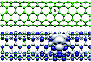
Carbon nanotubes whose inner hollow is filled with a metal have been studied for a long time. Filling CNTs was achieved soon after the discovery of CNTs when the capillary action of the tubes was used to fill them with liquid metals such as Pb.104 This was possibly the first metal–CNT composite ever made. Several experiments have been conducted since then to fill CNTs with liquid metals, resulting in interesting applications of these systems. For example, the thermal expansion of liquid gallium inside a MWNT has been used to build a ‘nanothermometer’ to measure the temperature on a very small spatial scale.105 Metal wires inside CNTs are also interesting for electrical applications, for example by using the metal wire as the electron conductor. The encapsulation in a CNT ensures the high aspect ratio of the metal that would otherwise tend to transform to the energetically more favourable spherical shape with a smaller surface. This has already been made use of by encapsulating Sn nanowires and by measuring their superconducting properties at low temperature.106The filling of MWNTs with solid metals has been carried out by using several techniques, e.g., by arc discharge,107,108CVD of metallocenes,109pyrolysis of organic compounds in the presence of metal catalysts,110 or condensed phase electrolysis.111Fig. 14 shows an example of a crystalline FeCo nanowire inside a MWNT. The interface between the tube and the metal is easily visible in electron microscopy images where the tube is seen in side-view. Occasionally, covalent bonds may exist at monolayer steps on the tube, i.e., where the innermost graphenic layers of the tube ends and forms bonds with the metal. Studies with a viewing direction along the axis have also been undertaken, but the interpretation of the projected images is difficult.112
 | ||
| Fig. 14 MWNT filled with a FeCo (alloy) crystal. The composite has been synthesized by CVD. (TEM image by J. A. Rodriguez-Manzo). | ||
Whereas numerous successful attempts have been undertaken to fill MWNTs with metals, the filling of SWNTs appears to be challenging. SWNTs have been filled with different inorganic compounds,113 but no report about metal-filled SWNTs has appeared until now. A study on double-wall carbon nanotubes showed that filling with Mo atoms is possible, but the Mo atoms form linear chains .114 The difficulty of filling SWNTs with metals is due to the narrow space inside the tube, allowing only highly unstable metallic nanowires of almost monoatomic thickness.
An interesting application of metal-filled tubes was found when the systems were subjected to electron irradiation. The displacement of carbon atoms in the CNT by ballistic knocks from the energetic electrons45 leads to a reconstruction of the graphitic lattice in such a way that the layers remain coherent but shrink continuously. Such a collapse of the tubes under the beam may exert a pressure of tens of GPa on the encapsulated metals.115 This has been made use of to study the plastic deformation of single metal nanocrystals inside graphitic cages.116 The metal wire can also slide inside the collapsing tube or be extruded, demonstrating that the bonding between the walls of the tubes and the transition metal crystal is weak. Electron irradiation of catalytically active metals (Fe, Co, Ni) encapsulated by a MWNT can also be used to study the growth of new tubes from the metal wires.81
Another application of metal–CNT systems is an electrically induced mass transport through the tubes. The transport of metals through carbon nanotubes has been achieved by electromigration when an electrical current flows through the metal filling inside a CNT.117–119 This has also been made use of to transport liquid metals from one tube to another tube in a ‘fluidic junction’120 and could constitute an element of a nanofluidic system. Metal particles on top of CNTs can also be transported under current flow through the tube.121
Metals on carbon nanotubes
The deposition of metals on the outer surface of CNTs is of interest for coating the tubes and making electrical contacts.122 Due to the weaker overlap of the π-orbitals protruding from the convex outer surface of the tubes, the interaction with metal atoms should be somewhat stronger than at the inner (concave) surface where the stronger π-overlap makes wetting more difficult. The first studies of metal deposition on CNTs were undertaken by chemical techniques.123,124 The deposition of metals was achieved by different routes, e.g., evaporation, sputtering, or electrochemical techniques. The formation of a continuous metal layer on the tube depends on good wetting of the surface with the metal. This has been tried by evaporating many different metals onto MWNTs.27 A continuous layer has been achieved for, e.g., Ti, Pd, or Pt, whereas Au or Pb do not wet the tube, and form islands. Annealing after deposition can improve the coverage, but Ostwald ripening may also take place, leading to even more pronounced island formation. It has been shown that Ni particles evaporated on the surface of CNTs lead to an electronic charge transfer and to the formation of bonds at the metal–carbon interface. Particles of noble metals, have also been deposited onto functionalized CNT surfaces that have been previously treated by an oxygen plasma to improve the bonding between metal and carbon.125 However, a considerable charge transfer between metal and carbon has not been detected in these systems.For several applications, e.g., in catalysis or in gas sensors,126 the formation of nanometre-sized metal particles on but also inside CNTs is desirable. Recent studies by tomographic imaging have shown that the deposition of metal particles on, as well as inside, CNTs is possible.127
Carbon nanotube-reinforced metals
Macroscopic composites of bulk metals with CNTs have been made for increasing the strength of metals against fracture and for improving their stability under repeated deformation. CNTs can be embedded into metals to pin dislocations and thus increase resistance against fatigue in a ‘conventional’ way. But CNTs can also be bonded to the metal matrix so that the high tensile strength of the tubes prevents the breakage of the material under load (without strong adhesion between metal matrix and CNTs, the favourable mechanical properties of CNTs cannot be made use of). The favourable elastic properties of CNTs and the absence of fatigue at moderate deformation would be another advantage in metal–CNT composites. Light-weight metals such as Al128 or Mg129 are of particular interest, but transition metals, e.g. Ni,130 have been studied as well. The mechanical properties of these composites often remained behind the expectations. This might be due to difficulties in the powder metallurgy processing where metal powders are mixed with CNTs and sintered. Recently, progress has been achieved, and the yield strength of some metals, e.g. Cu,131 could be increased by CNT reinforcement. The interest in metals as host materials for CNT reinforcement remained low, presumably because CNT-reinforced polymers are easier to produce and promise more applications.Outlook
Metals are the most important peripheral materials in carbon nanotube technology. Neither the reliable growth of CNTs nor the connection with an electrical or mechanical environment can at present be made without using metals. It is therefore mandatory that the interaction between these two completely different materials is understood in detail. The chemistry of metal–carbon bonding has been investigated for decades and is now well understood, but several aspects of the high anisotropy of graphenic structures, curved surfaces, or structural defects still need more experimental and theoretical work. It would be desirable to study the interaction of CNTs with as many different metals as possible in a systematic way.Establishing reliable electrical metal contacts on CNTs is a goal that has, to a large extent, already been achieved. Contacts with very low Ohmic resistance have been made, and the outstanding electrical properties of CNTs such as ballistic or quantum conductance would not have been accessible without good Ohmic or Schottky contacts. Present research therefore concentrates on the implementation of contacts into electronic circuits.
The technologies to create firm mechanical links between CNTs and metals are just being developed and depend on our ability to create covalently bonded end-contacts. Although this seems to work on the scale of individual tubes, an applicable technique on a large scale is still missing. A combination of end- and side-contacts, where covalent links are established not only at the open ends but also along a certain length of the side-wall, appears to be the most promising route. Electron beam-induced deposition has shown surprising results and could serve as a technique on a microscopic scale. A chemical procedure to activate the ends as well as the surface of CNTs and to link the bonds to metal crystals would be the key to implementing CNTs in macroscopic mechanical components such as ultrastrong ropes.
Although we already have a detailed picture from the role of metals in catalytic growth of CNTs, there are still many uncertainties, as is reflected by the fact that a reliable synthesis of CNTs with a predefined structure has yet to be achieved on a larger scale. The key to this challenge might be a thorough understanding of the chemical interaction of transition metals (single atoms as well as clusters or crystals) with graphenic layers and the role of physical processes such as solubility and diffusion.
Acknowledgements
The work of the author in the field of this review has been funded by grants from the Deutsche Forschungsgemeinschaft (Ba 1884/4-1 and Ba 1884/6-1) and from the Région Alsace (480-09). The author wishes to thank A. Krasheninnikov for commenting on the manuscript. The contribution of J. A. Rodríguez-Manzo to images in this article is gratefully acknowledged.Notes and references
-
R. Saito, G. Dresselhaus and M. S. Dresselhaus, Physical Properties of Carbon Nanotubes, Imperial College Press, London, 1999 Search PubMed
.
-
Understanding Carbon Nanotubes, Lecture Notes in Physics, ed. A. Loiseau, P. Launois, P. Petit, S. Roche and J.-P. Salvetat, 677, Springer, Berlin, Heidelberg, 2006 Search PubMed
-
Carbon Nanotubes, ed. A. Jorio, M. S. Dresselhaus and G. Dresselhaus, Springer, Berlin, 2007 Search PubMed
-
P. J. F. Harris, Carbon Nanotube Science, Cambridge University Press, Cambridge, 2009 Search PubMed
- K. S. Novoselov, D. Jiang, F. Schedin, T. J. Booth, V. V. Khotkevich, S. V. Morozov and A. K. Geim, Proc. Natl. Acad. Sci. U. S. A., 2005, 102, 10451 CrossRef CAS
- J.-C. Charlier, X. Blase and S. Roche, Rev. Mod. Phys., 2007, 79, 677 CrossRef CAS
- S. Tans, A. R. M. Verschueren and C. Dekker, Nature, 1998, 393, 49 CrossRef CAS
- P. Avouris, Acc. Chem. Res., 2002, 35, 1026 CrossRef CAS
- S. Heinze, J. Tersoff and P. Avouris, Lect. Notes Phys., 2006, 680, 381 Search PubMed
- F. Banhart, N. Grobert, M. Terrones, J.-C. Charlier and P. M. Ajayan, Int. J. Mod. Phys. B, 2001, 15, 4037 CrossRef CAS
- M. P. Anantram and F. Léonard, Rep. Prog. Phys., 2006, 69, 507 CrossRef CAS
- R. Vajtai, B. Q. Wei and P. M. Ajayan, Philos. Trans. R. Soc. London, Ser. A, 2004, 362, 2143 CrossRef CAS
-
B. T. Kelly, Physics of Graphite, Applied Science Publishers, London, 1981 Search PubMed
- J. J. Palacios, A. J. Pérez-Jiménez, E. Louis, E. SanFabián and Y. A. Vergéz, Phys. Rev. Lett., 2003, 90, 106801 CrossRef CAS
- N. Nemec, D. Tománek and G. Cuniberti, Phys. Rev. Lett., 2006, 96, 076802 CrossRef
- Y. Zhang, T. Ichihashi, E. Landree, F. Nihey and S. Iijima, Science, 1999, 285, 1719 CrossRef CAS
- J. Hu, M. Ouyang, P. Yang and C. Lieber, Nature, 1999, 399, 48 CrossRef CAS
- J. Luo, L. Zhang, Y. Zhang and J. Zhu, Adv. Mater., 2002, 14, 1413 CrossRef CAS
- K. Jensen, M. Mickelson, W. Han and A. Zettl, Appl. Phys. Lett., 2005, 86, 173107 CrossRef
- K. Asaka, H. Nakahara and Y. Saito, Appl. Phys. Lett., 2008, 92, 023114 CrossRef
- J. A. Rodríguez-Manzo, F. Banhart, M. Terrones, H. Terrones, N. Grobert, P. M. Ajayan, B. G. Sumpter, V. Meunier, M. Wang, Y. Bando and D. Golberg, Proc. Natl. Acad. Sci. U. S. A., 2009, 106, 4591 CrossRef CAS
- J. A. Rodríguez-Manzo, M. Wang, F. Banhart, Y. Bando and D. Golberg, Adv. Mater., 2009 Search PubMed
- D. Jiang, B. G. Sumpter and S. Dai, J. Am. Chem. Soc., 2006, 128, 6030 CrossRef CAS
- J. A. Rodríguez-Manzo, I. M. Janowska, C. Pham-Huu, A. Tolvanen, A. V. Krasheninnikov, K. H. Nordlund and F. Banhart, Small, 2009 Search PubMed
- A. Maiti and A. Ricca, Chem. Phys. Lett., 2004, 395, 7 CrossRef
- Y. Zhang, N. W. Franklin, R. C. Chen and H. Dai, Chem. Phys. Lett., 2000, 331, 35 CrossRef CAS
- Y. Zhang and H. Hai, Appl. Phys. Lett., 2000, 77, 3015 CrossRef CAS
- M. Menon, A. N. Andriotis and G. E. Froudakis, Chem. Phys. Lett., 2000, 320, 425 CrossRef CAS
- Y. Fan, B. R. Goldsmith and P. G. Collins, Nat. Mater., 2005, 4, 906 CrossRef CAS
- K. T. Chan, J. B. Neaton and M. L. Cohen, Phys. Rev. B: Condens. Matter Mater. Phys., 2008, 77, 235430 CrossRef
- A. V. Krasheninnikov, P. O. Lehtinen, A. S. Foster, P. Pyykkö and R. M. Nieminen, Phys. Rev. Lett., 2009, 102, 126807 CrossRef CAS
- H. L. Zhuang, G. P. Zheng and A. K. Soh, Comput. Mater. Sci., 2008, 43, 823 CrossRef CAS
- F. Banhart, J.-C. Charlier and P. M. Ajayan, Phys. Rev. Lett., 2000, 84, 686 CrossRef CAS
- F. Banhart, Ph. Redlich and P. M. Ajayan, Chem. Phys. Lett., 1998, 292, 554 CrossRef CAS
- K. Kong, Y. Choi, B.-H. Ryu, J.-O. Lee and H. Chang, Mater. Sci. Eng., C, 2006, 26, 1207 CrossRef CAS
- R. Anton and I. Schneidereit, Phys. Rev. B: Condens. Matter Mater. Phys., 1998, 58, 13874 CrossRef CAS
- Y. Gan, L. Sun and F. Banhart, Small, 2008, 4, 587 CrossRef CAS
-
W. Moffatt, The handbook of binary phase diagrams, Genium Publ. Corp., Schenectady, N. Y., 1976 Search PubMed
- M. Hasebe, H. Ohtani and T. Nishizawa, Metall. Trans. A, 1985, 16, 913 Search PubMed
-
Diffusion in Solid Metals and Alloys, ed. H. Mehrer, Landolt-Börnstein, New Series III/26, Springer, Berlin, 1990 Search PubMed
- R. B. McLellan, C. Ko and M. Wasz, J. Phys. Chem. Solids, 1992, 53, 1269 CrossRef CAS
- A. R. Harutyunyan, N. Awasthi, A. Jiang, W. Setyawan, E. Mora, T. Tokune, K. Bolton and S. Curtarolo, Phys. Rev. Lett., 2008, 100, 195502 CrossRef CAS
- B. Peng, M. Locascio, P. Zapol, S. Li, S. L. Mielke, G. C. Schatz and H. D. Espinosa, Nat. Nanotechnol., 2008, 3, 626 Search PubMed
- M.-F. Yu, O. Lourie, M. J. Dyer, K. Moloni, T. F. Kelly and R. S. Ruoff, Science, 2000, 287, 637 CrossRef CAS
- A. V. Krasheninnikov and F. Banhart, Nat. Mater., 2007, 6, 723 CrossRef CAS
- M. Huhtala, A. V. Krasheninnikov, J. Aittoniemi, S. J. Stuart, K. Nordlund and K. Kaski, Phys. Rev. B: Condens. Matter Mater. Phys., 2004, 70, 045404 CrossRef
- A. Kis, G. Csanyi, J.-P. Salvetat, T.-N. Lee, E. Couteau, A. J. Kulik, W. Benoit, J. Brugger and L. Forro, Nat. Mater., 2004, 3, 153 CrossRef CAS
- M. Buongiorno Nardelli, B. I. Yakobson and J. Bernholc, Phys. Rev. Lett., 1998, 81, 4656 CrossRef
- M.-F. Yu, M. C. Dyer, G. D. Skidmore, H. W. Rohrs, X. K. Lu, K.-D. Ausman, J. R. Von Ehr and R. S. Ruoff, Nanotechnology, 1999, 10, 244 CrossRef CAS
- M. Wang, Y. Bando, J. A. Rodríguez-Manzo, F. Banhart and D. Golberg, ACS Nano, 2009 DOI:10.1021/nn900634f
- M. S. Dresselhaus, G. Dresselhaus, J.-C. Charlier and E. Hernandez, Philos. Trans. R. Soc. London, Ser. A, 2004, 362, 2065 CrossRef CAS
- S. G. Louie, Top. Appl. Phys., 2001, 80, 113 CAS
- Y. Xue and M. A. Ratner, Appl. Phys. Lett., 2003, 83, 2429 CrossRef CAS
- W. Zhu and E. Kaxiras, Appl. Phys. Lett., 2006, 89, 243107 CrossRef
- Y. He, J. Zhang, S. Hou, Y. Wang and Z. Yu, Appl. Phys. Lett., 2009, 94, 093107 CrossRef
- F. Léonard and J. Tersoff, Phys. Rev. Lett., 2000, 84, 4693 CrossRef CAS
- A. Javey, J. Guo, Q. Wang, M. Lundstrom and H. Dai, Nature, 2003, 424, 654 CrossRef CAS
- Y. Yaish, J.-Y. Park, S. Rosenblatt, V. Sazonova, M. Brink and P. L. McEuen, Phys. Rev. Lett., 2004, 92, 046401 CrossRef CAS
- J. Appenzeller, J. Radoslavjevic, J. Knoch and P. Avouris, Phys. Rev. Lett., 2004, 92, 048301 CrossRef CAS
- S. J. Tans, M. H. Devoret, H. Dai, A. Thess, R. E. Smalley, L. J. Geerligs and C. Dekker, Nature, 1997, 386, 474 CrossRef CAS
- M. Bockrath, W. Liang, D. Bozovic, J. H. Hafner, C. M. Lieber, M. Tinkham and H. Park, Science, 2001, 291, 283 CrossRef CAS
- M. Buongiorno Nardelli, J.-L. Fattebert and J. Bernholc, Phys. Rev. B: Condens. Matter Mater. Phys., 2001, 64, 245423 CrossRef
- M. P. Anantram, S. Datta and Y. Xue, Phys. Rev. B: Condens. Matter Mater. Phys., 2000, 61, 14219 CrossRef CAS
- Q. Ngo, D. Petranovic, S. Krishnan, A. M. Cassell, Q. Ye, J. Li, M. Meyyappan and C. Y. Yang, IEEE Trans. Nanotechnol., 2004, 3, 311 CrossRef
- A. Kanda, Y. Ootuka, K. Tsukagoshi and Y. Aoyagi, Appl. Phys. Lett., 2001, 79, 1354 CrossRef CAS
- D. W. Austin, A. A. Puretzky, D. B. Geoghegan, P. F. Britt, M. A. Guillorn and M. L. Simpson, Chem. Phys. Lett., 2002, 361, 525 CrossRef CAS
- X. Cui, M. Freitag, R. Martel, L. Brus and P. Avouris, Nano Lett., 2003, 3, 783 CrossRef CAS
- B. Q. Wei, R. Vajtai and P. M. Ajayan, Appl. Phys. Lett., 2001, 79, 1172 CrossRef CAS
- D. Mann, A. Javey, J. Kong, Q. Wang and H. Dai, Nano Lett., 2003, 3, 1541 CrossRef CAS
- Z. Chen, J. Appenzeller, J. Knoch, Y.-M. Lin and P. Avouris, Nano Lett., 2005, 5, 1497 CrossRef CAS
- Y. Awano, S. Sato, D. Kondo, M. Ohfuti, A. Kawabata, N. Nihey and N. Yokoyama, Phys. Status Solidi A, 2006, 203, 3611 CrossRef CAS
- C. Berger, Y. Yi, J. Gezo, P. Poncharal and W. A. de Heer, New J. Phys., 2003, 5, 158 CrossRef
- N. Grobert, W. K. Hsu, Y. Q. Zhu, J. P. Hare, H. W. Kroto, D. R. M. Walton, M. Terrones, H. Terrones, Ph. Redlich, M. Rühle, R. Escudero and F. Morales, Appl. Phys. Lett., 1999, 75, 3363 CrossRef CAS
- P. O. Lehtinen, A. S. Foster, Y. Ma, A. V. Krasheninnikov and R. M. Nieminen, Phys. Rev. Lett., 2004, 93, 187202 CrossRef CAS
- E. J. G. Santos, A. Ayuela, S. B. Fagan, J. Mendes Filho, D. L. Azevedo, A. G. Souza Filho and D. Sánchez-Portal, Phys. Rev. B: Condens. Matter Mater. Phys., 2008, 78, 195420 CrossRef
-
In-Situ Electron Microscopy at High Resolution, ed. F. Banhart, World Sci. Publ., Singapore, 2008 Search PubMed
- S. Helveg, C. López-Cartes, J. Sehested, P. L. Hansen, B. S. Clausen, J. R. Rostrup-Nielsen, F. Abild-Petersen and J. K. Norskov, Nature, 2004, 427, 426 CrossRef CAS
- R. Sharma and Z. Iqbal, Appl. Phys. Lett., 2004, 84, 990 CrossRef CAS
- S. Hofmann, R. Sharma, C. Ducati, G. Du, C. Mattevi, C. Cepek, M. Cantoro, S. Pisanta, A. Parvez, F. Cervantes-Sodi, A. C. Ferrari, C. Dunin-Borkowski, S. Lizzit, L. Petaccia, A. Goldoni and J. Robertson, Nano Lett., 2007, 7, 602 CrossRef CAS
- H. Yoshida, S. Takeda, T. Uchiyama, H. Kohno and Y. Homma, Nano Lett., 2008, 8, 2082 CrossRef CAS
- J. A. Rodríguez-Manzo, M. Terrones, H. Terrones, H. W. Kroto, L. Sun and F. Banhart, Nat. Nanotechnol., 2007, 2, 307 Search PubMed
- Y. Shibuta and S. Maruyama, Chem. Phys. Lett., 2003, 382, 381 CrossRef CAS
- F. Ding, A. Rosén and K. Bolton, J. Chem. Phys., 2004, 121, 2775 CrossRef CAS
- J.-Y. Raty, F. Gygi and G. Galli, Phys. Rev. Lett., 2005, 95, 096103 CrossRef
- J. Zhao, A. Martinez-Limia and P. B. Balbuena, Nanotechnology, 2005, 16, S575 CrossRef
- J.-C. Charlier, H. Amara and Ph. Lambin, ACS Nano, 2007, 1, 202 CrossRef CAS
- H. Amara, C. Bichara and F. Ducastelle, Phys. Rev. Lett., 2008, 100, 056105 CrossRef CAS
- Y. Ohta, Y. Okamoto, S. Irle and K. Morokuma, ACS Nano, 2008, 2, 1437 CrossRef CAS
- O. Y. Yazyev and A. Pasquarello, Phys. Rev. Lett., 2008, 100, 156102 CrossRef
- J. Gavillet, A. Loiseau, C. Journet, F. Willaime, F. Ducastelle and J.-C. Charlier, Phys. Rev. Lett., 2001, 87, 275504 CrossRef CAS
- X. Fan, R. Buczko, A. A. Puretzky, D. B. Geoghegan, J. Y. Howe, S. T. Pantelides and S. J. Pennycook, Phys. Rev. Lett., 2003, 90, 145501 CrossRef CAS
- J. Gavillet, J. Thibault, O. Stéphan, H. Amara, A. Loiseau, Ch. Bichara, J.-P. Gaspard and F. Ducastelle, J. Nanosci. Nanotechnol., 2004, 4, 346 CrossRef CAS
- A. Thess, R. Lee, P. Nikolaev, H. Dai, P. Petit, J. Robert, C. Xu, Y. Hee, S. G. Kim, A. G. Rinzler, D. T. Colbert, G. E. Scuseria, D. Tománek, J. E. Fischer and R. Smalley, Science, 1996, 273, 483 CrossRef CAS
- P. K. de Bokx, A. J. H. M. Kock, E. Boellaard, W. Klop and J. W. Geus, J. Catal., 1985, 96, 454 CrossRef
- I. Alstrup, J. Catal., 1988, 109, 241 CrossRef CAS
- A. Maiti, C. J. Brabec and J. Bernholc, Phys. Rev. B: Condens. Matter Mater. Phys., 1997, 55, R6097 CrossRef CAS
- A. Schaper, H. Hou, A. Greiner and F. Phillipp, J. Catal., 2004, 222, 250 CrossRef CAS
- F. Abild-Pedersen, J. K. Norskov, J. R. Rostrup-Nielsen, J. Sehested and S. Helveg, Phys. Rev. B: Condens. Matter Mater. Phys., 2006, 73, 115419 CrossRef
- C. Jin, K. Suenaga and S. Iijima, Nat. Nanotechnol., 2008, 3, 17 Search PubMed
- J.-W. Snoeck, G. F. Froment and M. Fowles, J. Catal., 1997, 169, 240 CrossRef CAS
- S. Hofmann, G. Csanyi, A. C. Ferrari, M. C. Payne and J. Robertson, Phys. Rev. Lett., 2005, 95, 036101 CrossRef CAS
- R. T. K. Baker, T. S. Harris, R. B. Thomas and R. J. Waite, J. Catal., 1973, 30, 86 CAS
- F. S. Ou, M. M. Shaijumon, L. Ci, D. Benicewicz, R. Vajtai and P. M. Ajayan, Appl. Phys. Lett., 2006, 89, 243122 CrossRef
- P. M. Ajayan and S. Iijima, Nature, 1993, 361, 333 CrossRef CAS
- Y. Gao, Y. Bando, Z. Liu, D. Golberg and H. Nakanishi, Appl. Phys. Lett., 2003, 83, 2913 CrossRef CAS
- L. Jancovič, D. Gournis, P. N. Trikalitis, I. Arfaoui, T. Cren, P. Rudolf, M.-H. Sage, T. T. M. Palstra, B. Kooi, J. De Hosson, M. A. Karakassides, K. Dimos, A. Moukarika and T. Bakas, Nano Lett., 2006, 6, 1131 CrossRef CAS
- P. Guerret-Piécourt, Y. Le Bouar, A. Loiseau and H. Pascard, Nature, 1994, 372, 761 CrossRef CAS
- A. Loiseau and H. Pascard, Chem. Phys. Lett., 1996, 256, 246 CrossRef CAS
- C. N. R. Rao and S. Rahul, Chem. Commun., 1998, 1525 RSC
- N. Grobert, M. Terrones, O. J. Osborne, H. Terrones, W. K. Hsu, S. Trasobares, Y. Q. Zhu, J. P. Hare, H. W. Kroto and D. R. M. Walton, Appl. Phys. A: Mater. Sci. Process., 1998, 67, 595 CrossRef
- W. K. Hsu, M. Terrones, H. Terrones, N. Grobert, A. I. Kirkland, J. P. Hare, K. Prassides, P. D. Townsend, H. W. Kroto and D. R. M. Walton, Chem. Phys. Lett., 1998, 284, 177 CrossRef CAS
- N. Y. Jin-Phillipp and M. Rühle, Phys. Rev. B: Condens. Matter Mater. Phys., 2004, 70, 245421 CrossRef
- R. R. Meyer, J. Sloan, R. E. Dunin-Borkowski, A. I. Kirkland, M. C. Novotny, S. R. Bailey, J. L. Hutchison and M. L. H. Green, Science, 2000, 289, 1324 CrossRef CAS
- V. Meunier, H. Muramatsu, T. Hayashi, Y. A. Kim, D. Shimamoto, H. Terrones, M. S. Dresselhaus, M. Terrones, M. Endo and B. G. Sumpter, Nano Lett., 2009, 9, 1487 CrossRef CAS
- L. Sun, F. Banhart, A. V. Krasheninnikov, J. A. Rodriguez-Manzo, M. Terrones and P. M. Ajayan, Science, 2006, 312, 1199 CrossRef CAS
- L. Sun, A. V. Krasheninnikov, T. Ahlgren, K. Nordlund and F. Banhart, Phys. Rev. Lett., 2008, 101, 156101 CrossRef
- K. Svensson, H. Olin and E. Olsson, Phys. Rev. Lett., 2004, 93, 145901 CrossRef CAS
- D. Golberg, P. M. F. J. Costa, M. Mitome, S. Hampel, D. Haase, C. Mueller, A. Leonhardt and Y. Bando, Adv. Mater., 2007, 19, 1937 CrossRef CAS
- G. E. Begtrup, W. Gannett, J. C. Meyer, T. D. Yuzvinsky, E. Ertekin, J. C. Grossman and A. Zettl, Phys. Rev. B: Condens. Matter Mater. Phys., 2009, 79, 205409 CrossRef
- L. Dong, X. Tao, M. Hamadi, L. Zhang, X. Zhang, A. Ferreira and B. J. Nelson, Nano Lett., 2009, 9, 210 CrossRef CAS
- B. C. Regan, S. Aloni, R. O. Ritchie, U. Dahmen and A. Zettl, Nature, 2004, 428, 924 CrossRef CAS
- R. L. D. Whitby, W. K. Hsu, Y. Q. Zhu, H. W. Kroto and D. R. M. Walton, Philos. Trans. R. Soc. London, Ser. A, 2004, 362, 2127 CrossRef CAS
- T. W. Ebbesen, H. Miura, M. E. Bisher, M. M. J. Treacy, L. Shreeve-Keyer and R. C. Haushalter, Adv. Mater., 1996, 8, 155 CAS
- L. M. Ang, T. S. A. Hor, G. Q. Xu, C. H. Tung, S. P. Zhao and J. L. S. Wang, Carbon, 2000, 38, 363 CrossRef CAS
- A. Felten, C. Bittencourt and J. J. Pireaux, Nanotechnology, 2006, 17, 1954 CrossRef CAS
- E. H. Espinosa, R. Ionescu, C. Bittencourt, A. Felten, R. Erni, G. Van Tendeloo, J. J. Pireaux and E. Llobet, Thin Solid Films, 2007, 515, 8322 CrossRef CAS
- O. Ersen, J. Werckmann, O. Houllé, M.-J. Ledoux and C. Pham-Huu, Nano Lett., 2007, 7, 1898 CrossRef CAS
- T. Kuzumaki, K. Miyazawa, H. Ichinose and K. Ito, J. Mater. Res., 1998, 13, 2445 CAS
- C. S. Goh, J. Wei, L. C. Lee and M. Gupta, Nanotechnology, 2006, 17, 7 CrossRef CAS
- W. Chen, J. P. Tu, L. Y. Wang, H. Y. Gan, Z. D. Xu and X. B. Chang, Carbon, 2003, 41, 215 CrossRef CAS
- K. T. Kim, S. I. Cha, S. H. Hong and S. H. Hong, Mater. Sci. Eng., A, 2006, 430, 27 CrossRef
| This journal is © The Royal Society of Chemistry 2009 |