Identifying molecular signatures in metal-molecule-metal junctions
Makusu
Tsutsui
a,
Masateru
Taniguchi
*ab,
Kohei
Shoji
a,
Kazumichi
Yokota
a and
Tomoji
Kawai
*a
aThe Institute of Scientific and Industrial Research, Osaka University, Ibaraki, Osaka 567-0047, Japan. E-mail: taniguti@sanken.osaka-u.ac.jp; Fax: +81-6-6875-2440; Tel: +81-6-6879-8446
bPRESTO, Japan Science and Technology Agency, Honcho, Kawaguchi, Saitama 332-0012, Japan. Fax: +81-48-226-5651; Tel: +81-48-226-5601
First published on 2nd September 2009
Abstract
Single molecule identification in metal-molecule-metal junctions provides an ultimate probe that opens a new avenue for revolutionary advances in demonstrating single molecule device functions. Inelastic electron tunneling spectroscopy (IETS) is an ultra-sensitive method for probing vibrational characteristics of molecules with atomic resolution. State-of-the-art experiments on the inelastic transport in self-assembled monolayers of organic molecules have demonstrated the utility of the IETS technique to derive structural information concerning molecular conformations and contact configurations. Here we report the vibrational fingerprint of an individual π-conjugated molecule sandwiched between gold nanoelectrodes. Our strategy combines analyses of single molecule conductance and vibrational spectra exploiting the nanofabricated mechanically-controllable break junction. We performed IETS measurements on 1,4-benzenedithiol and 2,5-dimercapto-1,3,4-thiadiazole to examine chemical discrimination at the single-molecule level. We found distinct IET spectra unique to the test molecules that agreed excellently with the Raman and theoretical spectra in the fingerprint region, and thereby succeeded in electrical identification of single molecule junctions.
Introduction
Fundamental understanding of electron transport through a single molecule is an important step toward realizing practical applications of metal-molecule-metal junctions as building blocks for future nanoelectronics. Significant progress in single molecule electrical characteristic measurements has been achieved in the past decade,1–3 owing to the various reliable techniques developed for fabricating molecular junctions, such as cross-bar junctions,4,5 nanopore systems,6,7 electromigration break junctions,8–10 and mechanical break junctions.11–18 It has now been well established that the conductance of single molecule junctions with a relatively large energy gap at the frontier molecular orbital levels and the electrode Fermi level decays exponentially with the length of the molecules,2 manifesting electron tunneling in the junctions. Recent theoretical calculations have also been successful in reproducing the experimental electron transmissivity.19 Transport in molecular junctions has thus been recognized to be fully unraveled in the elastic tunneling regime.19On the other hand, fascinating molecular signatures become observable in the tunneling junctions under high field where inelastic tunneling comes into play.20 At biases Vb > ħω/e, where ω and e are the characteristic molecular vibration mode frequency and the electron charge, a few electrons are allowed to impart the kinetic energy to the degree of freedom of molecular vibration motions, thereby opening a new channel for electron transmission that leads to a small increment of the junction conductance. Generally, vibration modes that couple strongly to electrons are inherent to molecules. Therefore, probing the conductance changes associated with inelastic electron tunneling enables chemical identification of individual molecules. This technique is known as inelastic electron tunneling spectroscopy (IETS), which has been extensively utilized to elucidate the chemical nature of single molecules adsorbed on one side of a metal substrate in the study field of surface science.21–23 The potential of IETS as a unique probe for addressing electron-molecular vibration interactions at the single-molecule level can serve as a powerful tool for showing clear-cut evidence that assumed metal-molecule-metal structures of a specific geometry have actually been formed,20,24,25 an essential ingredient for reliable single molecule measurements. The unique capability would also enable the detection of chemical reactions and molecular adsorptions/desorptions at the single-molecule level.
The attractive ability of IETS has led to keen interest in examining the spectroscopy measurements on metal-molecule-metal systems. State-of-the-art experiments4,5,7,26–28 have proven that IETS is applicable to molecular junctions by reporting vibrational spectra of self-assembled monolayers of organic molecules sandwiched between two metal substrates. Recently, IETS measurements of single organic molecule junctions have also been examined.29 Notwithstanding the sophisticated work reported to date, however, interpretation of IET spectra is still often complicated since even selection rules are yet to be established. Thus, further effort should be devoted to explore to what extent we can expect IETS measurements to provide chemical information about single molecule junctions.
Our aim here is to apply this vibrational analysis to demonstrate electrical discrimination of two different single organic molecule junctions so as to verify its capability for detecting single molecule fingerprints in metal-molecule-metal systems. Although the formation of stable molecular junctions is a vital prerequisite for reliable IETS measurements, we have recently developed a ‘self-breaking’ method using nanofabricated mechanically-controllable break junctions (nano-MCBJs) that fulfils the technical criterion.30–32 We employed 1,4-benzenedithiol (BDT) and 2,5-dimercapto-1,3,4-thiadiazole (DMcT) as test molecules (Fig. 1(f)). These π-conjugated molecules were chosen because of the similarity in their physical properties, such as the molecular length and the HOMO-LUMO gap, while possessing different vibrational characteristics, an important condition facilitating interpretation and direct comparison of experimental spectra.
 | ||
| Fig. 1 Structure of nano-MCBJs and test molecules. (a) Scanning electron microscopy image of nano-MCBJs. (b) Magnified view of the narrowest region. Typical cross section was approximately 100 nm (width) × 80 nm (thickness). (c) A free-standing metal junction fractured by bending the substrate from the rear with a pushing rod. By so doing, a pair of nanoelectrodes was formed. (d) Further manipulation of beam bending permits fine adjustment of the gap distance between the electrodes at sub-picometer resolution. This unique advantage of nano-MCBJ enables the formation of highly-stable molecular junctions. (e) Schematic illustration of a single molecule junction consisting of a single molecule contacted on both sides to metal electrodes. (f) 1,4-benzenedithiol (BDT) and 2,5-dimercapto-1,3,4-thiadiazole (DMcT) were employed as test molecules. | ||
Experimental
Fabrication of nano-MCBJs
Nano-MCBJ samples were prepared by the following procedures.31,33 A phosphorous bronze substrrte was first coated with a thin layer of polyimide (thickness ∼ 4 µm) for insulation. We then patterned nano-scale junctions on the substrate by a standard electron beam lithography process. After that, Au nanojunctions were obtained by carrying out metal deposition (Cr 1 nm/Au 80 nm) via radio-frequency magnetron sputtering and subsequent lift-off. Finally, the polyimide underneath the Au junctions was removed by isotropic reactive ion etching (CF4 : O2 = 1 : 5, 50 W), and a free-standing Au nanobridge was formed. The scanning electron micrograph in Fig. 1(a) shows the typical geometry of the junctions.Formation of stable molecular junctions using the self-breaking technique
A nano-MCBJ sample is placed on a sample holder mounted on a cryostat cold head, which can be cooled to 4.2 K. The sample substrate was then bent mechanically in order to break the nanojunctions (Fig. 1(b–d)) in a dilute toluene solution of BDT or DMcT (0.01 mM). As a consequence, the fresh fracture surface at the nanoconstriction was exposed to the molecular solution, which allows molecule adsorption on the junction. Subsequently, the sample chamber was evacuated. When the vacuum level reached ∼10−5 Torr, we started to open/close the junctions repeatedly by manipulating the beam bending through piezo-actuator motion control. Meanwhile, the junction conductance was monitored using a fast digital oscilloscope (Waverunner, LeCroy Co.) and a picoammeter (Keithley 6487). The sequential nanocontact forming/breaking processes were regulated using the automated resistance feedback control; we finely tuned the junction stretching speed so as to reproducibly form stable molecular junctions (self-breaking method).30–32IETS measurements of single molecule junctions
Forming and holding a junction at the single molecule conductance, dI/dVb was measured using a lock-in technique. For this purpose, a lock-in modulation of 10 mV at 1 kHz was added to Vb using a home-built voltage adder. Vb was swept from −0.23 V to 0.23 V. The current was amplified using a preamplifier. The output signal was then read by a lock-in amplifier (SR830, Stanford Research Systems) and the first harmonic was recorded using a data acquisition card (NI USB-9234, National Instruments). The IET spectrum was acquired numerically from the recorded dI/dVb–Vb characteristics.Results and discussion
Single molecule conductance of BDT and DMcT
Single molecule conductance measurements were performed by repeatedly forming molecular junctions through manipulating displacements of the MCBJ electrodes to move in and out of contact with each other. The junction conductance exhibited a series of stepwise decreases during mechanical stretching. A long flat plateau emerged reproducibly at around 1 G0. This is a well-established characteristic signifying the formation of Au single atom contacts, which have a fully-open single channel for electron transmission.34 On pulling it further, the atom-sized junction eventually ruptured and conductance often demonstrated exponential decay to zero suggesting electron tunnelling across a vacuum gap. In other cases, we observed an additional conductance plateau below 1 G0. Typical traces acquired for BDT and DMcT are compared in Fig. 2(a). The corresponding conductance histograms reveal multiple-peak structures (Fig. 2(b,c)). We confirmed that such pronounced peaks were completely absent in conductance histograms when we add no molecules. Therefore, the low conductance states are ascribable to the electrical properties of the metal-molecule-metal junctions. The low-G peaks emerge at quantized levels with spacings of 0.011 G0 and 0.008 G0 for BDT and DMcT, respectively. These regular peaks are naturally interpreted as denoting the number of molecules bridging the electrodes.13 The lowest peak conductance, GBDT = 0.011 G0 and GDMcT = 0.008 G0, thus represents the single molecule conductance (it is noted that GBDT agrees with the single molecule conductance reported for Au-BDT-Au junctions in a previous study35). | ||
| Fig. 2 Single molecule conductance measurements for BDT and DMcT. (a) Typical conductance curves during junction breaking recorded at room temperature in a vacuum under a constant d.c. bias voltage of 0.2 V for Au–Au (black), Au-BDT-Au (purple), and Au-DMcT-Au (blue) junctions. Stretching speed is set to 6 pm/s. The conductance was recorded on a logarithmic scale for clear visualization of the entire breaking process starting from thinning of a fused Au junction to the eventual rupture of single molecule junctions. (b) Corresponding conductance histograms of BDT (purple) and (c) DMcT (blue) with traces revealing clear step structures at the low-G regime below 1 G0 (412 and 475 traces out of 1000 traces for BDT and DMcT, respectively). The histograms are characterized by three peaks positioned at integer multiples of GBDT(DMcT) = 0.011 (0.008) G0. Yellow lines are Gaussian fits to the peak profiles. | ||
It is not unexpected that BDT and DMcT share similar electrical conductivity. In general, electron transmittance in metal-metal junctions is determined by the carrier injection barrier at metal-molecule interfaces. Closer alignment of the molecular HOMO (or LUMO) level to the gold Fermi level leads to stronger electronic coupling due to larger overlap of the molecular orbital and the gold Fermi level orbital.36 As a result, electronic states become more delocalized giving rise to a lower barrier at the contacts. Our molecular orbital calculations predict that the difference in the HOMO-LUMO gap between BDT and DMcT is marginal with the former being larger by only ∼50 meV. Therefore, the fact that GBDT ∼ GDMcT is, at least within this simple picture, consistent with the expected little difference in the energy gaps between the frontier molecular orbital levels and the metal electrode Fermi level.
Thus far, the single molecule conductance measurements allow quantitative characterization and reliable control of the number of molecules trapped between the nanoelectrodes. Furthermore, a distinct difference in the single molecule conductance between BDT and DMcT indicates that the observed electrical characteristics are intrinsic molecular properties. Nevertheless, as any characteristics unique to the tested molecules have not been addressed directly, there still a lack of clear-cut evidence for validating the successful formation and measurement of single molecule junctions.
IET spectra of single molecule junctions at 4.2 K
The capability to identify molecule species in single molecule junctions provides unambiguous proof for elucidating that the measured electrical characteristics are of single molecule origin. Here, we performed a proof-of-principle demonstration of single molecule identification through IETS analyses of the two different organic molecules. We first conducted repeated formation/breakdown of molecular junctions at room temperature for hundreds of cycles. After confirming the reproducible evolution of well-defined conductance plateaus at around GBDT or GDMcT, we slowly cooled the sample to 4.2 K. The repeated junction formation/breakdown processes were resumed during the sample cooling. After the temperature stabilized at 4.2 K, we formed a single molecule junction by the self-breaking method at a stretching rate of 6 pm/s using GBDT(DMcT) as a marker at Vb = 0.2 V (Fig. 3). We have demonstrated in our previous work that the single molecule junction conductance is temperature independent in the tunneling regime.37 Thus, it is expected that GBDT(DMcT) remains constant down to 4.2 K. We froze the piezo-actuator motion at a point when G approached GBDT(DMcT). dI/dVb was then scanned over a Vb range from −0.23 V to 0.23 V using a lock-in technique. After each measurement, we fused the contact to above 1 G0 and formed a new single molecule junction of a different configuration using the self-breaking method. | ||
| Fig. 3 Formation of single molecule junctions of BDT (purple) and DMcT (blue) at 4.2 K using the self-breaking technique. The junction stretching speed is set to 6 pm/s. The broken lines indicate GBDT (purple) and GDMcT (blue). The piezo-actuator motion was frozen when G approached GBDT(DMcT) to hold the molecular junctions. | ||
Typical dI/dVb–Vb curves are shown in Fig. 4(a,b). Qualitatively, BDT and DMcT show similar characteristics; the differential conductance exhibits a stepwise increase with |Vb|. The dI/dVb staircase manifests the contributions of inelastic electron transport in addition to elastic tunneling at Vb above a threshold with each dI/dVb step representing the opening of an active inelastic channel associated with electronic excitation of a molecular vibration mode.
 | ||
| Fig. 4 Single molecule IET spectra of BDT and DMcT measured at 4.2 K. dI/dVb–Vb characteristics of (a) BDT and (b) DMcT single molecule junctions reveal stepwise increases in the differential conductance at a specific Vb reflecting contributions of inelastic electron tunnelling at Vb > ħω/e. The corresponding vibration spectra are displayed for (c) BDT and (d) DMcT. Four representative peaks detected in each spectrum are labelled. | ||
It is noted that the curve is not symmetric with respect to zero bias. The slight asymmetry stems presumably from the fact that metal-molecule coupling at the right and left electrodes is not identical but differs to some extent, which gives rise to different electron–phonon coupling strengths at positive and negative Vb.
IET spectra of BDT and DMcT are obtained numerically from the dI/dVb–Vb characteristics in Fig. 4(a,b). The spectra are fairly symmetric with respect to bias polarity and dominated by several peaks at Vp that signify the excitation of particular molecular vibrations with energy ħω = eVpvia inelastic electron tunneling processes (Fig. 4(c,d)).
Vibrational mode assignment for BDT single molecule junctions based on Raman spectroscopy measurements and model calculations
We examined vibrational mode assignment on the basis of Raman spectra and theoretical calculations (Fig. 5). Raman spectroscopic measurements were performed on a self-assembled monolayer at room temperature using a He/Ne beam (632.8 nm). We observed a good agreement in the obtained spectra with the previous reports.38–41 Model calculations of the active molecular vibration modes were conducted using the DFT method with BLYP exchange–correlation functionals obtained from the generalized gradient approximation. The 6-31G(d,p) basis set was used for H, C, N, and S atoms, and a Lanl2dz basis set was used for the Au atoms. All calculations were performed using the GAUSSIAN03 program.42 Four distinct modes of vibration were found to strongly couple with conducting electrons for each type of molecule (Fig. 5). Table 1 lists the vibrational modes and the frequencies obtained from the two control experiments together with the IETS peak positions in the positive Vb range of the spectrum shown in Fig. 4(c). The spectrum of a BDT junction plausibly illustrates the unique vibrational signatures. The pronounced peaks at 196 mV (1582 cm−1), 139 mV (1122 cm−1), and 86 mV (694 cm−1) represent excitations of νs(C![[double bond, length as m-dash]](https://www.rsc.org/images/entities/char_e001.gif) C) {1574 cm−1 [1598 cm−1]}, δs(C–C–H) {1190 cm−1 [1138 cm−1]}, and δs(C–C–C) {742 cm−1 [832 cm−1]} in the phenyl ring, respectively, where we use the notation {ωRaman [ωcalculation]} to denote the reference vibration mode frequencies. There also appears a peak centered at 45 mV (363 cm−1). The most possible candidate for the low-bias peak is νs(Au–S) {341 cm−1 [404 cm−1]}. Consequently, all the peaks, especially those assigned to on-molecule vibration modes, are in excellent agreement with the experimental Raman spectrum, thereby achieving IETS fingerprinting of BDT single molecule junctions.
C) {1574 cm−1 [1598 cm−1]}, δs(C–C–H) {1190 cm−1 [1138 cm−1]}, and δs(C–C–C) {742 cm−1 [832 cm−1]} in the phenyl ring, respectively, where we use the notation {ωRaman [ωcalculation]} to denote the reference vibration mode frequencies. There also appears a peak centered at 45 mV (363 cm−1). The most possible candidate for the low-bias peak is νs(Au–S) {341 cm−1 [404 cm−1]}. Consequently, all the peaks, especially those assigned to on-molecule vibration modes, are in excellent agreement with the experimental Raman spectrum, thereby achieving IETS fingerprinting of BDT single molecule junctions.
| Molecule | Peak No. | Peak position | Raman (Calculation) cm−1 | Vibration modes | |
|---|---|---|---|---|---|
| mV | cm−1 | ||||
| BDT | 1 | 45 | 363 | 341 (404) | νs(Au–S) |
| 2 | 86 | 694 | 742 (832) | δs(C–C–C) | |
| 3 | 139 | 1122 | 1190 (1138) | δs(C–C–H) | |
| 4 | 196 | 1582 | 1574 (1598) | νs(CC) |
|
| DMcT | 5 | 26 | 210 | 376 (242) | νs(Au–S) |
| 6 | 80 | 646 | 579 (581) | δs(C–S–C) | |
| 7 | 128 | 1033 | 1044 (1049) | νs(NN) |
|
| 8 | 168 | 1356 | 1450 (1380) | νs(CN) |
|
 | ||
| Fig. 5 Raman spectra of (a) BDT and (b) DMcT were obtained at room temperature using a He/Ne laser (632.8 nm). Accuracy of the spectral measurement was estimated to be better than 1 cm−1. Active vibrational modes of (c) BDT and (d) DMcT contributing to IETS deduced from model calculations. Vibrational frequencies were calculated for a single molecule bridged between gold clusters composed of 13 gold atoms using the density function theory method with the BLYP exchange–correlation functional obtained from the generalized gradient approximation. The 6-31G(d,p) basis set was used for H, C, N, and S atoms, and a Lanl2dz basis set was used for Au atoms. All calculations were performed using the GAUSSIAN03 program. | ||
Discrimination of BDT and DMcT single molecule junctions viaIETS
Having attained single BDT molecule identification in metal-molecule-metal junctions, we now discuss the discrimination of two different molecule species, BDT and DMcT, based on the vibrational spectra. As we have seen in Fig. 4(c,d), the general appearance of the molecular spectrum is analogous to the BDT counterpart. However, there is an obvious discrepancy in the peak positions, reflecting different electron–phonon coupling in the two molecules. The most clear distinction lies in that the three peaks assigned to the phenyl vibration modes of BDT are absent in the spectrum of DMcT. Instead, new peaks arise at 168 mV (1356 cm−1), 128 mV (1033 cm−1), and 80 mV (646 cm−1), the Vp of which can be assigned to νs(CN) {1450 cm−1 [1380 cm−1]}, νs(N–N) {1044 cm−1 [1049 cm−1]}, and δs(C–S–C) {579 cm−1 [581 cm−1]}. At even lower bias regime lies a sharp peak at 26 mV (210 cm−1), which presumably belongs to νs(Au–S) {376 cm−1 [242 cm−1]}.
The relatively large uncertainty in peak assignment of the low-energy vibration modes to the Raman peaks is not unexpected. In principle, IETS is different from Raman spectroscopy in that the former probes molecular vibration-induced changes in the frontier orbital electronic energy level whereas the latter detects electric field-stimulated dipole moments. Exact selection rules for IETS are yet to be established. However, theory predicts that Raman-forbidden out-of-plane modes with frequency below 800 cm−1 may contribute to the IET spectrum.43 The out-of-plane vibration manifolds thus complicate the interpretation of the low-frequency experimental IET spectrum and pose difficulties in specifying correct modes to the observed low-bias peak. Overall, however, the two different single molecule junctions are readily distinguishable from the IET spectra in the fingerprint region of 1600 cm−1 to 600 cm−1.
Temperature dependence of vibrational spectra
The clear dI/dVb–Vb staircase as well as the good accordance of Vp to the Raman-active vibrational mode energy suggest that the measured electrical characteristics are indeed intrinsic signatures of the test molecules. Nevertheless, we still lack solid evidence to validate that the peculiar dI/dVb steps are ascribable to inelastic electron tunneling. Therefore, we attempted to characterize thermal smearing effects in the IET spectrum.
IETS measurements were extended to high temperatures up to 20 K for a DMcT single molecule junction that provided the dI/dVb–Vb characteristics of Fig. 4(b). As presented in Fig. 6(a), the dI/dVb–Vb curve reveals clear dI/dVb steps even at 20 K, while it seems likely that the stepwise feature is becoming more blunt as we increase the temperature. We deduced the IET spectrum from each dI/dVb–Vb curve (Fig. 6(b)). As can be seen in the figure, the line shape of the spectra remains unchanged over the temperature range measured. In order to evaluate possible peak broadening via thermal smearing, we extracted the full-width at half-maximum (FWHM) of the two peaks in the middle, peaks assigned to νs(NN) and δs(C–S–C), by Gaussian fitting and plotted them as a function of the temperature (Fig. 7). We find that the peak width tends to become expanded with increasing temperature. Theory predicts that the width of vibrational peaks increases linearly with the temperature as 5.4kBT/e by Fermi distribution smearing.44–46 In the present case, we obtain the rate of peak expansion of ∼10kBT/e by linear fit to the plots in Fig. 7, which agrees with the theoretical value within a factor of two. This finding serves to verify that the experimental d2I/dVb2–Vb characteristics are genuine vibrational spectra of single DMcT molecules anchored to Au nanoelectrodes.
 | ||
| Fig. 6 Temperature dependence of a single molecule IET spectrum. (a) dI/dVb–Vb characteristics and (b) corresponding vibrational spectra of an individual DMcT single molecule junction measured in a temperature range from 4.2 K to 20 K. | ||
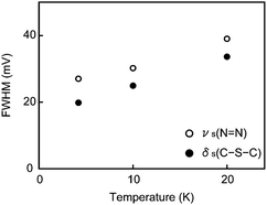 | ||
| Fig. 7 Temperature dependence of νs(NN) and δs(C–S–C) peak widths. | ||
Conclusions
We have demonstrated single molecule identification in metal-molecule-metal junctions by revealing a clear correspondence of the molecular vibrational spectra to the Raman spectroscopy counterparts. We find that molecular junctions consisting of different types of molecules can be distinguished from their IET spectra. Furthermore, thermal smearing-induced vibrational peak broadening is investigated to ensure that the experimental d2I/dVb2–Vb characteristics are indeed molecular signatures intrinsic to the single molecule junctions. As a result, the peaks are found to become broadened with increasing temperature at a rate that accords with a theoretical prediction, supporting that the dI/dVb steps and the corresponding peak profile observed in the d2I/dVb2–Vb curves are molecular signatures reflecting inelastic electron-molecular vibration interactions under current flow.Notes and references
- A. Nitzan and M. A. Ratner, Science, 2003, 300, 1384 CrossRef CAS.
- N. J. Tao, Nat. Nanotechnol., 2006, 1, 173 Search PubMed.
- M. Galperin, M. A. Ratner, A. Nitzan and A. Troisi, Science, 2008, 319, 1056 CrossRef CAS.
- J. G. Kushmerick, J. Lazorcik, C. H. Patterson and R. Shachidhar, Nano Lett., 2004, 4, 639 CrossRef.
- J. M. Beebe, H. J. Moore, T. R. Lee and J. G. Kushmerick, Nano Lett., 2007, 7, 1364 CrossRef CAS.
- W. Wang, T. Lee and M. A. Reed, Phys. Rev. B: Condens. Matter Mater. Phys., 2003, 68, 035416 CrossRef.
- W. Wang, T. Lee, I. Kretzschmar and M. A. Reed, Nano Lett., 2004, 4, 643 CrossRef CAS.
- H. Park, J. Park, A. K. L. Lim, E. H. Anderson, A. P. Alivisatos and P. L. McEuen, Nature, 2000, 407, 57 CrossRef.
- W. Liang, M. P. Shores, M. Bockrath, J. R. Long and H. Park, Nature, 2002, 417, 725 CrossRef CAS.
- E. A. Osorio, K. O'Neill, N. Stuhr-Hansen, O. F. Nielsen, T. Bjørnholm and H. S. J. van der Zant, Adv. Mater., 2007, 19, 281 CrossRef CAS.
- M. A. Reed, C. Zhou, C. J. Muller, T. P. Burgin and J. M. Tour, Science, 1997, 278, 252 CrossRef CAS.
- R. H. M. Smit, Y. Noat, C. Untiedt, N. D. Lang, M. C. van Hemert and J. M. van Ruitenbeek, Nature, 2002, 419, 906 CrossRef CAS.
- B. Xu and N. J. Tao, Science, 2003, 301, 1221 CrossRef CAS.
- Z. Huang, F. Chen, R. D'Agosta, P. A. Bennett, M. Di Ventra and N. J. Tao, Nat. Nanotechnol., 2007, 2, 698 Search PubMed.
- L. Venkataraman, J. E. Klare, I. W. Tam, C. Nuckolls, M. S. Hybertsen and M. L. Steigerwald, Nano Lett., 2006, 6, 458 CrossRef CAS.
- L. Venkataraman, J. E. Klare, C. Nuckolls, M. S. Hybertsen and M. L. Steigerwald, Nature, 2006, 442, 904 CrossRef.
- S. Y. Quek, M. Kamenetska, M. L. Steigerwald, H. J. Choi, S. G. Louie, M. S. Hybertsen, J. B. Neaton and L. Venkataraman, Nat. Nanotechnol., 2009, 4, 230 Search PubMed.
- S. Wu, M. T. GonzÁlez, R. Huber, S. Grunder, C. Schönenberger, M. Mayor and M. Calame, Nat. Nanotechnol., 2008, 3, 569 Search PubMed.
- S. M. Lindsay and M. A. Ratner, Adv. Mater., 2007, 19, 23 CrossRef CAS.
- M. Galperin, M. A. Ratner and A. Nitzan, J. Phys.: Condens. Matter, 2007, 19, 103201 CrossRef.
- B. C. Stipe, M. A. Razaei and W. Ho, Science, 1998, 280, 1732 CrossRef CAS.
- T. Komeda, Y. Kim, M. Kawai, B. N. J. Persson and H. Ueba, Science, 2002, 295, 2055 CrossRef CAS.
- J. I. Pascual, N. Lorente, Z. Song, H. Conrad and H. P. Rust, Nature, 2003, 423, 525 CrossRef CAS.
- A. Troisi and M. A. Ratner, Small, 2006, 2, 172 CrossRef CAS.
- M. Kula, J. Jiang and Y. Luo, Nano Lett., 2006, 6, 1693 CrossRef CAS.
- N. Okabayashi, Y. Konda and T. Komeda, Phys. Rev. Lett., 2008, 100, 217801 CrossRef.
- M. Rahimi and M. Hegg, Phys. Rev. B: Condens. Matter Mater. Phys., 2009, 79, 81404 CrossRef.
- H. Song, Y. Kim, J. Ku, Y. H. Jang, H. Jeong and T. Lee, Appl. Phys. Lett., 2009, 94, 103110 CrossRef.
- J. Hihath, C. R. Arroyo, G. Rubio-Bollinger, N. J. Tao and N. Agraït, Nano Lett., 2008, 8, 1673 CrossRef.
- M. Tsutsui, K. Shoji, M. Taniguchi and T. Kawai, Nano Lett., 2008, 8, 345 CrossRef CAS.
- M. Tsutsui, M. Taniguchi and T. Kawai, Nano Lett., 2008, 8, 3293 CrossRef CAS.
- M. Tsutsui, K. Shoji, M. Taniguchi and T. Kawai, Appl. Phys. Lett., 2008, 92, 223110 CrossRef.
- J. M. van Ruitenbeek, A. Alvarez, I. Pineyro, C. Grahmann, P. Joyez, M. H. Devoret, D. Esteve and C. Urbina, Rev. Sci. Instrum., 1996, 67, 108 CrossRef CAS.
- N. Agraït, A. L. Yeyati and J. M. van Ruitenbeek, Phys. Rep., 2003, 377, 81 CrossRef CAS.
- X. Xiao, B. Xu and N. J. Tao, Nano Lett., 2004, 4, 267 CrossRef CAS.
- L. Venkataraman, Y. S. Park, A. C. Whalley, C. Nuckolls, M. S. Hybertsen and M. L. Steigerwald, Nano Lett., 2007, 7, 502 CrossRef CAS.
- M. Tsutsui, M. Taniguchi and T. Kawai, Nano Lett., 2009, 9, 2433 CrossRef CAS.
- S. H. Cho, H. S. Han, D.-J. Jang, K. Kim and M. S. Kim, J. Phys. Chem., 1995, 99, 10594 CrossRef CAS.
- S. W. Joo, S. W. Han and K. Kim, J. Colloid Interface Sci., 2001, 240, 391 CrossRef CAS.
- H. G. M. Edwards, A. F. Johnson and E. E. Lawson, J. Mol. Struct., 1995, 351, 51 CrossRef CAS.
- F. Hipler, S. G. Girol, W. Azzam, R. A. Fischer and C. Wöll, Langmuir, 2003, 19, 6072 CrossRef CAS.
- M. J. Frisch, G. W. Trucks, H. B. Schlegel, G. E. Scuseria, M. A. Robb, J. R. Cheeseman, J. A. Montgomery Jr., T. Vreven, K. N. Kudin, J. C. Burant, J. M. Millam, S. S. Lyengar, J. Tomasi, V. Barone, B. Mennucci, M. Cossi, G. Scalmani, N. Rega, G. A. Petersson, H. Nakatsuji, M. Hada, M. Ehara, K. Toyota, R. Fukuda, J. Hasegawa, M. Ishida, T. Nakajima, Y. Honda, O. Kitao, H. Nakai, M. Klene, X. Li, J. E. Knox, H. P. Hratchian, J. B. Cross, C. Adamo, J. Jaramillo, R. Gomperts, R. E. Stratmann, O. Yazyev, A. J. Austin, R. Camml, C. Pomelli, J. W. Ochterski, P. Y. Ayala, K. Morokuma, G. A. Voth, P. Salvador, J. J. Dannenberg, V. G. Zakrzewski, S. Dapprich, A. D. Daniels, M. C. Strain, O. Farkas, D. K. Malick, A. D. Rabuck, K. Raghavachari, J. B. Foresman, J. V. Ortiz, Q. Cui, A. G. Baboul, S. Clifford, J. Cioslowski, B. B. Stefanov, G. Liu, A. Liashenko, P. Piskorz, I. Komaromi, R. L. Martin, D. J. Fox, T. Keith, M. A. Al-Laham, C. Y. Peng, A. Nanayakkara, M. Challacombe, P. M. W. Gill, B. Johnson, W. Chen, M. W. Wong, C. Gonzalez, J. A. Pople, Gaussian03, revisionC.02; Gaussian, Inc.: Pittsburgh, PA, 2003 Search PubMed.
- A. Troisi and M. A. Ratner, Nano Lett., 2006, 6, 1784 CrossRef CAS.
- J. Lambe and R. C. Jaklevic, Phys. Rev. B, 1967, 165, 821 Search PubMed.
- A. S. Hällback, N. Oncel, J. Huskens, H. J. W. Zandvliet and B. Poelsema, Nano Lett., 2004, 4, 2393 CrossRef.
- W. Wang, T. Lee and M. A. Reed, J. Phys. Chem. B, 2004, 108, 18398 CrossRef CAS.
| This journal is © The Royal Society of Chemistry 2009 |