Self-assembled CNT circuits with ohmic contacts using Pd hexadecanethiolate as in situ solder†
Thiruvelu
Bhuvana‡
a,
Kyle C.
Smith
b,
Timothy S.
Fisher
*b and
Giridhar U.
Kulkarni
*a
aChemistry and Physics of Materials Unit and DST Unit on Nanoscience, Jawaharlal Nehru Centre for Advanced Scientific Research, Jakkur P O, Bangalore, 560 064, India. E-mail: kulkarni@jncasr.ac.in
bDepartment of Mechanical Engineering and Birck Nanotechnology Center, Purdue University, West Lafayette, IN 47907-2057, USA. E-mail: tsfisher@purdue.edu
First published on 16th September 2009
Abstract
An easy and elegant method of CNT nanocircuit fabrication using a metal organic precursor of Pd, namely, Pd hexadecanethiolate, is presented. This precursor directs the self-assembly of individual CNTs spanning a gap between Au electrodes. This is achieved by first patterning the precursor along the edges of the gap electrodes, as it enables direct patterning by e beam. Further, thermal activation of the precursor at 250 °C leads to metallization and the ohmic electrical contact between the CNTs and the electrodes beneath. A resistive fuse action of the soldered CNTs is observed as well.
1. Introduction
Carbon nanotubes (CNTs), because of their unique electrical, mechanical and other interesting properties, have been projected as prototype building blocks of nanoscale architectures.1 While applications involving random collections of CNTs are relatively straightforward to develop and study, the exploitation of the properties of individual CNTs has remained a daunting task, given that CNTs are too large for chemical manipulation and rather small for mechanical grippers! Accordingly much research activity has focused on CNT manipulation.2 An important aspect of this activity is the fabrication of electrical circuits with CNTs as active elements mechanically coupled to electrodes. There are at least two pertinent questions raised in this context, namely addressing of a CNT and the nature of coupling with its electrode. This article describes a method by which CNTs are made to self-assemble across electrodes through passive interaction with a patterned Pd-containing precursor that is subsequently converted, by simple thermolysis, to an interconnected dense collection of Pd nanoparticles. The latter are shown to provide ohmic-like contact between the electrode surface and the CNTs.Among the investigated methods for contacting CNTs, one may differentiate those in which individual or a set of CNTs are addressed from a random or an orderly collection spread over a substrate, from those wherein CNTs are deposited only onto desired locations. The former methodology is time intensive as it involves multiple steps: locating a CNT using a microscopy tool, marking its location and finally depositing electrodes. This is usually achieved by performing electron (or ion) beam induced metal deposition (EBID or FIBID) facilitated by a scanning electron microscope or by shadow masking prior to physical vapor deposition.3–6 Instead of metal deposition, there are a few reports where movable microcantilevers served as contacting electrodes.7,8 Langford et al.9 have discussed the various methods for electrical contacts on CNTs, and Yaglioglu et al.10 have studied means of characterising sheet and contact resistance.
Several methods have been reported in the literature for the deposition of CNTs at desired locations, using approaches such as chemical functionalisation and self-assembly. For instance, Lewenstein et al.5 fabricated circuits by amino-functionalising the metal electrodes whereas LeMieux et al.11 functionalised the gap between the electrode. Klinke et al.12 used functionalised CNTs which were placed in designated areas, and electrodes were built subsequently over each adsorbed CNT. Using AFM for manipulation, Gao et al.13 placed an individual CNT between two opposing metal electrodes and realised a four-point arrangement using two additional CNTs. Li et al.14 made use of a PDMS microchannel mold and directed SWNTs into channels under gas pressure to transfer them between a pair of gap electrodes. Using a catalyst bed beneath an anodised alumina membrane, Maschmann et al.15 successfully grew vertical SWNTs through the pores and established top contact by electroplating Pd nanocubes. Another commonly employed method is dielectrophoresis, in which the electric dipole of a CNT exposed to an inhomogeneous electric field is made to guide a CNT to a specific electrode location.16,17
Despite these innovations to make CNT circuits, contact resistance reduction at the CNT-electrode interface remains an active area of research. Bachtold et al.18 exposed a prefabricated CNT-Au electrode system to the electron beam in a SEM chamber to improve the contact resistance between a CNT and Au electrode. The contact resistance was reduced by several orders of magnitude due to exposure to the e-beam. EBID19,20 has also been employed to create metal deposits at CNT-electrode junctions effectively to serve as solder material. Though such deposits are not truly metallic,21 they do improve contact. In another study, Au nanoparticlesol was used as an ink to write as a ‘fountain pen’ at contacts.22 Contacts between CNTs and metal electrodes can also be improved by rapid thermal annealing.23
The present work is aimed at building single CNT circuits, primarily through a self-assembly process in contrast to those previously discussed. Electrode regions are selectively coated with a metal precursor, Pd hexadecanethiolate, employing a direct write method,24 which motivated this work. Following the deposition of CNTs, the precursor is easily metallised by thermolysis to serve as a solder in situ, thus establishing a reliable ohmic contact.
2. Results and discussion
2.1 Self-assembling CNT across gap electrodes
A specialty with the gap electrodes used in this work is that the electrode edges forming the gap were deposited with Pd hexadecanethiolate by e beam patterning (see Fig. 1). A drop of CNT dispersion on patterned gap electrodes produced a circuit with nine CNTs across the 200 µm long Au electrodes as shown in the SEM image of Fig. 2. The linear density of bridging CNTs is expected to depend on the CNT concentration, which was kept constant at 5 mg CNTs in 125 mL of carbon tetrachloride. The nine CNTs shown in Fig. 2 represent the highest such density observed among seven trials. We note that no large-scale bundling of bridging CNTs was observed in any trial. The magnified images reveal that the CNTs assemble nearly perpendicularly with respect to the axis of the gap with very similar overlaps on both electrodes. While most bridges consist of individual CNTs, in two locations several are entangled. The CNTs are well spaced from each other laterally. Typical spacing between the CNTs is 20 μm. Further, no CNT was observed to lie longitudinally inside the gap region, nor did any lie solely on a single electrode in any trial. | ||
| Fig. 1 Scheme of the procedure adopted. (a) Au gap electrodes, (b) Pd hexadecanethiolate is patterned on Au electrodes along the edges, (c) after dropping the CNT dispersion, the CNTs self-assemble across the gap and (d) the CNTs are soldered by simply activating the patterned thiolate. | ||
 | ||
| Fig. 2 SEM image of the Au gap electrodes after drop casting with CNTs along with its schematic (a) with and (b) without Pd hexadecanethiolatepatterning along the electrode. In (a), zoom-in images are shown as insets. SEM images were taken in 0.1 Torr of water vapor/N2 (environmental mode) in order to avoid local charging of the glass substrate. While electrode regions are clear, some local charging is seen in the gap region. | ||
The above observations are indeed striking given that this self-assembly involves no external direction; such a circumstance is highly desired for CNT-based circuits. It is also surprising to see several individual CNTs across the gap electrodes while the dispersion itself was found to contain, as expected, highly entangled bundles of CNTs. In the absence of Pd hexadecanethiolatepatterning, CNTs deposited over Au electrode regions have disordered orientation (see Fig. 2b). The test with the patterned precursor, Pd hexadecanethiolate, clearly involves a self-assembly process. Following repetitive experiments, we have found that nearly 80% of the tubes in the vicinity of electrodes (i.e., within 10 µm) assemble across gap electrodes; otherwise, the tubes exhibit random orientation such as shown on the left side of the SEM image in Fig. 2b. Similar observations have been reported on PDMS stamp surfaces,25 where CNTs self-assemble across stamp microchannels. In this case, a similar mechanism is likely active whereby the channel region forms a pool of solvent that is the last to evaporate. As the liquid front recedes into this channel, alignment of CNTs occurs such that they are perpendicular to the front and thus finally bridge the channel because the CNT length exceeds the size of the channel width. Further, in this case, Pd hexadecanethiolate is itself a hydrophobic self-assembling molecule,26 and consequently, its presence may produce preferential surface interactions with the hydrophobic CNTs. The present approach offers an additional and important advantage that the precursor can be converted to an electrically conductive contact as described in the following.
2.2 Soldering self-assembled CNTs
The precursor, Pd hexadecanethiolate, undergoes metallisation around 250 °C. The resulting species contains low carbon impurity and exhibits conductivity close to the bulk value (see ESI, Fig. S1† ). This observation prompted the application of the precursor as a solder material. I-V measurements were performed on the CNT circuit shown in Fig. 2. The I-V curve shape was non-linear (Fig. 3a) with the current in the range of nA. This is clearly due to the insulating action of the patterned precursor prior to thermolysis.24 Such a state was also encountered with a carbon fibre circuit in the presence of interpenetrating Pd precursor (see ESI, Figs. S2 and S3† ). The finite current observed in the CNT circuit arises likely from the nanometric thickness of the dielectric precursor. The dielectric character of the Pd precursor is reflected in the form of charge saturation in I-V measurements. Following thermolysis at 250 °C, the I-V relation became highly linear (Fig. 3b) with a resistance of 48.8 kΩ, illustrating that conduction through the CNT-solder-electrode contact is ohmic. The resistance of this circuit is higher but within an order of magnitude of the total resistances measured by Lan et al.27 for 130–225 nm diameter CNTs across a gap of 10 µm. Because CNT resistivity is known to depend strongly on growth conditions and diameter, contact resistance cannot be directly inferred from a resistance measurement alone. To assess contact quality, direct measurements of contact resistance and CNT resistivity are currently being pursued using the method of Lan et al.27 The above results indicate the possibility of producing self-assembled individual ohmic CNT circuits. Indeed, in another attempt using a dilute CNT dispersion, a single CNT circuit was realized (Fig. 4). Following soldering, the I-V data exhibited a linear response (Fig. 4b) with a resistance of 4.9 kΩ which is of the order of a single MWCNT resistance.5 Additionally, three such circuits have been realized (see ESI, Fig. S4† ).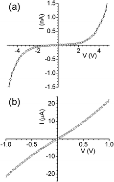 | ||
| Fig. 3 I-V characteristics of (a) CNTs self-assembled across the gap and (b) after thermolysis at 250 °C for 10 minutes. | ||
 | ||
| Fig. 4 (a) SEM image of a CNT on the cross-linked Pd precursor (marked Pd) on Au electrodes (the gap is blurred due to local charging while imaging). (b) I-V characteristics after thermolysis at 250 °C for 10 minutes. | ||
The CNT circuits thus fabricated are indeed nanometric resistors. The Joule heating of CNTs is typically of the order of 10–100 µW and is enough to cause a temperature rise of hundreds of degrees Celsius.28;29 Under such conditions, CNTs can undergo burn out. One such example is the circuit shown in Fig. 2, with examples of CNT-based fuse action in Fig. 5a and b. In these examples, the CNTs seem to burn out in the middle due to high current. The observation of failure in the CNT device region (Fig. 5a and b) rather than in the contacts further indicates the low electrical resistance of the contacts and diffusive nature of the electrical conduction;30,31 in addition, some favorable annealing may occur in the contact regions under self heating such that the interface resistance decreases both electrically and thermally. Under uniform self-heating of a cylinder with negligible electrical contact resistance, the maximum temperature rise will occur at its centre. The fact that the observed failure occurs very near the exact centre of the CNT device suggests that the heat generation profile is relatively symmetric. The magnitude of maximum temperature rise depends on local electrical heat generation, CNT diameter, contact width between the CNT and substrate material in the gap between electrodes, span of the gap, and specific thermal contact conductance in the gap. Using a simple diffuse mismatch model to estimate the specific thermal contact conductance32 and calculating contact width with a plane-strain adhesive contact model,33 we estimate that a local heat generation rate per unit CNT length of 120 W/m is required to bring about air oxidation of a 150 nm diameter CNT centrally lying on a 9 µm SiO2 gap (assuming that the thermal oxidation in air takes place at 700 °C34). Local heat generation depends strongly on applied bias and the temperature-dependent resistivity of a CNT. Future measurements of CNT resistivity will aid evaluation of the model and in quantitative prediction of breakdown voltages.
 | ||
| Fig. 5 SEM images of blown off CNTs from Fig. 2a while applying excess external bias. | ||
3. Experimental
Several Au gap electrodes (50 nm thick) were deposited on glass slides using thin carbon fibres as shadow masks under physical vapor deposition (Fig. 1). The gaps were typically 9 µm wide. The obtained electrodes were coated with a 200 nm film of Pd hexadecanethiolate, Pd(SC16H35)2, by spin-coatingca. 100 µL toluene solution (1 mM) at 2000 rpm. Initially, the thiolate precursor was prepared by mixing an equimolar ratio of Pd acetate and hexadecanethiol, both dissolved in toluene. Following the reaction, the solution became viscous, and the yellow color deepened to orange-yellow.26 The obtained thiolate was washed with methanol and acetonitrile to remove excess thiol and finally dissolved in toluene. Electron beam lithography (EBL) was performed over the deposited film covering ca. 5 µm wide rectangular regions along the gap electrode edges (see Fig. 1) using a Nova NanoSEM 600 instrument (FEI Co., The Netherlands) at an electron beam energy of 5 kV and dosage of 54 µC cm−2.24,35 After patterning, the resist was developed in toluene for 10 seconds and dried under flowing argon.Multi-walled carbon nanotubes (Sigma Aldrich) of diameters 150–300 nm and lengths 7–12 µm were used as active elements across the gap electrodes. The CNTs were dispersed in carbon tetrachloride solution by ultrasonication for 30 minutes. A 10 µL amount of the CNT dispersion was drop-cast upon the patterned substrate. Carbon tetrachloride was chosen as the medium for nanotube dispersion, not just because the nanotubes form a good dispersion in it but also because the patterns do not get washed away as the Pd hexadecanethiolate is insoluble in this solvent. In a few standardisation experiments (see ESI† ), carbon fibres (diameter 7–8 µm and length ca. 5 mm) were placed between Au electrodes on glass plate (gap width ca. 1.1 mm) using forceps, and Pd hexadecanethiolate was either spin-coated prior to fibre placement or drop-coated on top. In all current–voltage characteristics measurements, a Keithley 236 multimeter served as the source and measurement unit.
4. Conclusion
The passive self-assembly and subsequent nanosoldering action of Pd hexadecanethiolate has been demonstrated on multi-walled CNTs, which is easily extendable to single-walled CNTs. A striking feature of CNT circuits developed in this study is that CNTs have placed themselves in a highly desired configuration with an in situ generated nanocrystalline Pd solder derived from the thiolate precursor. This method should enable facile fabrication of circuits with single CNTs. The integrity and low resistance of the ultimate metallic contacts is demonstrated by the observation that the CNT device regions were burned out in the centre, rather than near the contacts. This approach to create self-aligning and moderate-temperature metallic contacting of CNTs suggests many possible applications and extensions, including CNT interconnects, fuses, thin-film transistors, and chemical sensors.Acknowledgements
The authors thank Professor C. N. R. Rao for his encouragement. The financial support from the Department of Science and Technology, Government of India, and the National Science Foundation (NSF-USA) is gratefully acknowledged. KCS thanks NSF-USA for financial support in the form of a graduate research fellowship.References
- R. H. Baughman, A. A. Zakhidov and W. A. de Heer, Science, 2002, 297, 787 CrossRef CAS; C. N. R. Rao and A. Govindaraj, Nanotubes and Nanowires, Royal Society of Chemistry, London, 2007 Search PubMed.
- M. Yu, M. J. Dyer, G. D. Skidmore, H. W. Rohrs, X. Lu, K. D. Ausman, J. R. V. Ehr and R. S. Ruoff, Nanotechnology, 1999, 10, 244 CrossRef CAS.
- T. W. Ebbesen, H. J. Lezec, H. Hiura, J. W. Bennett, H. F. Ghaemi and T. Thio, Nature, 1996, 382, 54 CrossRef CAS.
- C. Schönenberger, A. Bachtold, C. Strunk, J.-P. Salvetat and L. Forró, Appl. Phys. A: Mater. Sci. Process., 1999, 69, 283 CrossRef CAS.
- J. C. Lewenstein, T. P. Burgin, A. Ribayrol, L. A. Nagahara and R. K. Tsui, Nano Lett., 2002, 2, 443 CrossRef CAS.
- S. Dohn, K. Mølhave, D. N. Madsen, R. Mateiu, P. Bøggild, A. M. Rasmussen, M. Brorson and C. J. H. Jacobsen, Mater. Res. Soc. Symp. Proc., 2003, 772, 153 CAS.
- S. Dohn, K. Mølhave and P. Bøggild, Sens. Lett., 2005, 3, 300 CrossRef CAS.
- P. J. de Pablo, M. T. Martnez, J. Colchero, J. Gomez-Herrero, W. K. Maser, A. M. de Benito, E. Munoz and A. M. Baro, Mater. Sci. Eng., C, 2001, 15, 149 CrossRef.
- R. M. Langford, T.-X. Wang, M. Thornton, A. Heidelberg, J. G. Sheridan, W. Blau and R. Leahy, J. Vac. Sci. Technol., B, 2006, 24, 2306 CrossRef CAS.
- O. Yaglioglu, A. J. Hart and R. Martens, Rev. Sci. Instrum., 2006, 77, 095105 CrossRef.
- M. C. LeMieux, M. Roberts, S. Barman, Y. W. Jin, J. M. Kim and Z. Bao, Science, 2008, 321, 101 CrossRef CAS.
- C. Klinke, J. B. Hannon, A. Afzali and P. Avouris, Nano Lett., 2006, 6, 906 CrossRef CAS.
- B. Gao, Y. F. Chen, M. S. Fuhrer, D. C. Glattli and A. Bachtold, Phys. Rev. Lett., 2005, 95, 196802 CrossRef CAS.
- S. Li, N. Liu, M. B. Chan-Park, Y. Yan and Q. Zhang, Nanotechnology, 2007, 18, 455302 CrossRef.
- M. R. Maschmann, A. D. Franklin, A. Scott, D. B. Janes, T. D. Sands and T. S. Fisher, Nano Lett., 2006, 6, 2712 CrossRef CAS.
- T. Schwamb, T. Y. Choi, N. Schirmer, N. R. Bieri, B. Burg, J. Tharian, U. Sennhauser and D. Poulikakos, Nano Lett., 2007, 7, 3633 CrossRef CAS.
- A. Vijayaraghavan, S. Blatt, D. Weissenberger, M. Oron-Carl, F. Hennrich, D. Gerthsen, H. Hahn and R. Krupke, Nano Lett., 2007, 7, 1556 CrossRef CAS.
- A. Bachtold, M. Henny, C. Terrier, C. Strunk, C. Schönenberger, J. P. Salvetat, J. M. Bonard and L. Forró, Appl. Phys. Lett., 1998, 73, 274 CrossRef CAS.
- D. N. Madsen, K. Mølhave, R. Mateiu, A. M. Rasmussen, M. Brorson, C. J. H. Jacobsen and P. Bøggild, Nano Lett., 2003, 3, 47 CrossRef CAS.
- T. Brintlinger, M. S. Fuhrer, J. Melngailis, I. Utke, T. Bret, A. Perentes, P. Hoffmann, Abourida and P. Doppelt, J. Vac. Sci. Technol., B, 2005, 23, 3174 CrossRef CAS.
- A. Botman, J. J. L. Mulders, R. Weemaes and S. Mentink, Nanotechnology, 2006, 17, 3779 CrossRef CAS.
- C. P. R. Dockendorf, M. Steinlin, D. Poulikakos and Choi, Appl. Phys. Lett., 2007, 90, 193116 CrossRef.
- J. O. Lee, C. Park, J. J. Kim, J. Kim, J. W. Park and K. H. Yoo, J. Phys. D: Appl. Phys., 2000, 33, 1953 CrossRef CAS.
- T. Bhuvana and G. U. Kulkarni, ACS Nano, 2008, 2, 457 CrossRef CAS.
- J. Chen and W. A. Weimer, J. Am. Chem. Soc., 2002, 124, 758 CrossRef CAS.
- P. J. Thomas, A. Lavanya, V. Sabareesh and G. U. Kulkarni, Proc.–Indian Acad. Sci., Chem. Sci., 2001, 113, 611 Search PubMed.
- C. Lan, P. Srisungsitthisunti, P. B. Amama, T. S. Fisher, X. Xu and R. G. Reifenberger, Nanotechnology, 2008, 19, 125703 CrossRef.
- M. Steiner, M. Freitag, V. Perebeinos, J. C. Tsang, J. P. Small, M. Kinoshita, D. Yuan, J. Liu and P. Avouris, Nat. Nanotechnol., 2009, 4, 320 Search PubMed.
- R. A. Sayer, S. Kim, A. D. Franklin, S. Mohammadi and T. S. Fisher, IEEE Trans. Components Packag. Technol., submitted Search PubMed.
- D. G. Cahill, K. Goodson and A. Majumdar, J. Heat Transfer, 2002, 124, 223 CrossRef CAS.
- J. P. Small, L. Shi and P. Kim, Solid State Commun., 2003, 127, 181 CrossRef.
- E. T. Swartz and R. O. Pohl, Rev. Mod. Phys., 1989, 61, 605 CrossRef.
- J. Baney and C.-Y. Hui, J. Adhes. Sci. Technol., 1997, 11, 393 CrossRef CAS.
- P. M. Ajayan, T. W. Ebbesen, T. Ichihashi, S. Iijima, K. Tanigaki and H. Hiura, Nature, 1993, 362, 522 CrossRef CAS.
- T. Bhuvana, L. Gregoratti, S. Heun, M. Dalmiglio and G. U. Kulkarni, Langmuir, 2009, 25, 1259 CrossRef CAS.
Footnotes |
| † Electronic supplementary information (ESI) available: Details of the thermolysis of Pd hexadecanethiolate and preliminary results on carbon fibre as active element between the gap electrodes. See DOI: 10.1039/b9nr00035f |
| ‡ Present address: Purdue University, West Lafayette, IN 47907-2057, USA. |
| This journal is © The Royal Society of Chemistry 2009 |