Integration of femtosecond laser written optical waveguides in a lab-on-chip
Rebeca Martinez
Vazquez
a,
Roberto
Osellame
*a,
Daniela
Nolli
a,
Chaitanya
Dongre
b,
Hans
van den Vlekkert
c,
Roberta
Ramponi
a,
Markus
Pollnau
b and
Giulio
Cerullo
a
aIstituto di Fotonica e Nanotecnologie - CNR, Dipartimento di Fisica - Politecnico di Milano, Piazza L. da Vinci, 32, 20133, Milano, Italy. E-mail: roberto.osellame@polimi.it
bIntegrated Optical MicroSystems, MESA+ Institute for Nanotechnology, University of Twente, PO Box 217, 7500 AE Enschede, The Netherlands
cLioniX BV, PO Box 456, 7500 AL Enschede, The Netherlands
First published on 6th November 2008
Abstract
We use direct femtosecond laser writing to integrate optical waveguides into a commercial fused silica lab-on-chip (LOC). We fabricate high quality waveguides intersecting the microfluidic channels and use them to optically address with high spatial selectivity their content. Fluorescence from the photoexcited volume is efficiently collected at a 90° angle by a high numerical aperture fiber, resulting in a compact and portable setup. Our approach is quite powerful because it allows the integration of photonic functionalities, by simple post-processing, into commercial LOCs, fabricated with standard techniques. By taking advantage of the unique three-dimensional capabilities of femtosecond laser writing, more complex functionalities, such as splitters or Mach–Zehnder interferometers, can be implemented.
1. Introduction
Lab-on-chips (LOCs) are rapidly becoming fundamental tools in many applications,1–3 ranging from basic science (genomics and proteomics), to chemical synthesis and drug developments,4 high-throughput medical and biochemical analysis,5 environmental monitoring and detection of chemical and biological threats.While many different fluidic functions have already been implemented on LOCs, a key unsolved problem is the development of an integrated on-chip detection system.6 The main reason for this deficiency is that, as the size of the microfluidic systems shrinks, also the detection volumes become smaller, thereby decreasing the number of molecules available for detection. Therefore, the integrated detection system should also provide a very high sensitivity. Electrochemical and optical are the two most widespread detection schemes for LOCs. Optical measurements are superior both in terms of flexibility and sensitivity; in particular, laser-induced fluorescence (LIF) detection of labelled molecules, being a background-free technique, allows the measurement of very low analyte concentrations.
In traditional setups used in conjunction with LOCs, both excitation and detection are performed using bulk optical elements, such as mirrors, lenses and microscope objectives, to focus the excitation light into a tiny measurement volume and to collect the resulting fluorescence. Such schemes require accurate mechanical alignment to the microfluidic channels, are more sensitive to mechanical vibrations and drifts and allow only a limited number of detection configurations. The requirement of coupling a miniaturized LOC system with a massive benchtop instrument, such as an optical microscope, frustrates many of the LOC advantages, in particular strongly limiting device portability and preventing field or point-of-care applications. Much of the commercial success of the LOC concept will critically depend on the ability to successfully integrate optical detection schemes.
A strong research activity is currently devoted to the task of on-chip integration of micro-optical components.7–16 In particular optical waveguides allow confinement and transport of light in the chip, directing it to a small volume of the microfluidic channel and collecting the emitted/transmitted radiation. However, the fabrication of optical waveguides or more complex photonic components integrated with the microfluidic channels is not a straightforward process, since it requires a localized increase of the refractive index of the substrate. Depending on the substrate of choice, several techniques are possible (for example silica on silicon,8–10 ion exchange,11,12 or polymers16), all of which however are multistep and include photolithography, thus considerably complicating the LOC fabrication process. A microfabrication technique capable of easily integrating optical waveguides in LOCs is therefore highly in demand. The integration on the same substrate of optical and microfluidic components has far-reaching scientific and technological implications that go beyond the specific application; to define this new research field, the terms “optofluidics” has been recently introduced in the scientific literature.17,18
Recently, a novel technique for the direct writing of waveguides and photonic circuits in transparent glass substrates, exploiting nonlinear refractive index modifications induced by focused femtosecond pulses, has emerged.19,20 The basic physical mechanisms underlying this process can be outlined as follows: when a femtosecond pulse is tightly focused in a transparent material, a nonlinear absorption mechanism, combining multiphoton and avalanche ionization, allows deposition of energy in a small volume around the focus, where the intensity is the highest.21 The photogenerated hot electron plasma induces high temperatures and pressures that give rise to different phenomena such as densification, direct photostructural modifications and colour centers formation; under suitable conditions, the combination of such effects may lead to a local increase of refractive index over a micrometer-sized volume of the material. By moving the laser focus inside the substrate one can use the laser beam to define regions of increased index and thus directly produce three-dimensional light-guiding structures.
Compared with traditional techniques, femtosecond waveguide writing offers two striking advantages for integrated optics: (i) it is a direct maskless fabrication technique: one can take a glass chip and create in a single step, by moving it with respect to the laser beam focus, single optical waveguides or more complicated photonic devices (splitters, interferometers, etc.); (ii) it has unique three-dimensional capabilities, since it allows to define waveguides at arbitrary depths inside the glass. So far, this technique has been almost exclusively applied to the manufacturing of optical waveguides for telecom photonic devices.22,23 However, it appears highly suited for the integration of optical waveguides into LOCs. In fact, it is possible to locate optical waveguides at arbitrary positions inside a microfluidic device, thus avoiding intersection (if required) between waveguide and channel or between waveguides by offsetting the structures at different depths; in this way more compact layouts are feasible and much more freedom in the design is possible. In addition, it can be applied to an already fabricated LOC without affecting the layout and the manufacturing procedure of the microfluidic part of the device, thus greatly simplifying the production process (in particular the sealing of the device) and taking advantage of the several already-well-developed designs for microfluidic chips. Finally, the flexibility of this technology brings significant advantages in terms of rapid prototyping and customization of the optofluidic devices; in fact, once the microfluidic performance is assessed, the position and the number of waveguides providing the excitation/collection of light can be experimentally optimized in a very easy way or varied on demand according to the customer needs.
In this paper we demonstrate the integration of femtosecond laser written optical waveguides into a commercial LOC for capillary electrophoresis (CE). We fabricate high quality waveguides intersecting the microfluidic channels and use them to optically address with high spatial selectivity their contents. Fluorescence from the optically excited volume is efficiently collected at a 90° angle by a high numerical aperture fiber, resulting in a highly compact and portable setup.
Section 2 describes the femtosecond laser waveguide fabrication setup, presents the optical characteristics of waveguides fabricated in fused silica and explains the procedure for integrating the waveguides in the LOC, crossing the microfluidic channels. Section 3 describes the experimental setup used for LIF and presents a measurement of the limit of detection (LOD). Finally, Section 4 presents the conclusions and perspectives for future developments.
2. Optical waveguide fabrication
2.1 Femtosecond laser waveguide fabrication in fused silica
Fig. 1 shows the experimental setup used for femtosecond laser optical waveguide fabrication in glass. It starts with a regeneratively amplified Ti:sapphire laser (model CPA-1, Clark Instrumentation) producing 150 fs, 500 µJ pulses at 1 kHz repetition rate and 800 nm wavelength. A fraction of the laser pulse energy ranging from 2 to 5 µJ, controlled by a variable attenuator, is used for waveguide writing. The pulses are focused by a low numerical aperture microscope objective (NA = 0.3) at a depth variable from 0.2 to 1 mm inside the glass. The samples are moved by a precision translation stage (Physik Instrumente model M-155.11), at speeds ranging from 10 to 100 µm/s, perpendicularly to the beam propagation direction (transverse writing geometry). This geometry gives the greatest fabrication flexibility but has the drawback of producing waveguides with strongly asymmetric cross section, since the confocal parameter b = 2πw02/λ is much longer than the focal diameter d = 2w0. This problem can be overcome by introducing a focusing geometry in which the femtosecond writing beam is astigmatically shaped by changing both the spot sizes in the tangential and sagittal planes and the relative positions of the beam waists.24 This shaping allows one to modify the interaction volume in such a way that the waveguide cross section can be made circular and with arbitrary size. The astigmatic beam shaping can be easily obtained by a cylindrical telescope; fine control of the distance between the cyclindrical lenses is used to tune the offset between the beam waists and thus the waveguide cross section.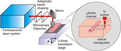 | ||
| Fig. 1 Experimental setup for femtosecond laser waveguide writing. | ||
We initially optimized the waveguide fabrication process on plain fused silica substrates similar to those used for the LOC production. Fig. 2 shows top (a) and side (b) images, acquired with a differential interference contrast microscope, of an optical waveguide fabricated with 4 µJ pulse energy and a translation speed of 20 µm/s. This rather low fabrication speed may be considered the main limitation of this fabrication technology. It should be noted that much higher speeds have been demonstrated with higher repetition rate lasers;23 however, even with the above value, a 4 mm waveguide is manufactured in each chip in about 3 minutes. The modified volume presents a circular cross section, with a diameter of approximately 10 µm. It should be noted that, in this fabrication regime, the material modification is limited to the focal volume of the writing beam. This is important for our application since the relative position of optical waveguide and microfluidic channel is critical, calling for a fine control of position and shape of the modified region. Optical characterization of the waveguides showed that they are single-mode in the visible, as demonstrated by the near field of the mode profile measured at the wavelength of 543 nm, reported in Fig. 2(c). Single mode operation is not strictly necessary for single waveguide fluorescence excitation; however, it provides reduced bending losses in optical splitters for multi-point excitation and will allow the fabrication of interferometers for label-free sensing. The refractive index change was measured with a near-field profilometer (Rinck Elektronik) and a value of 7 × 10⁻⁴ at 650 nm was obtained.25 This value is in good agreement with the results of a calculation using a numerical mode solver software (BeamPROP 4.0, RSoft) to reproduce the measured waveguide mode. This low refractive index change implies a limited numerical aperture of the waveguide (NA ∼ 0.05). As will be discussed in the following this is beneficial for uniform excitation through the microchannel. Nevertheless, the refractive index change may be increased, with different irradiation parameters, up to ∼ 1 × 10−2.26 Propagation losses at 543 nm were measured using the cut-back technique and were found to be 0.9 dB cm−1 (see Fig. 2(d)). This value is very promising as compared to those obtained at similar wavelengths on other kinds of waveguides integrated on LOCs and fabricated with SU-8 polymer (lit.,11 2.5 dB cm−1), SiON (lit.,10 1 dB cm−1), or liquid core (lit.,12 1.8 dB cm−1) technologies. Even lower values of propagation losses can be foreseen with improved translation stages.
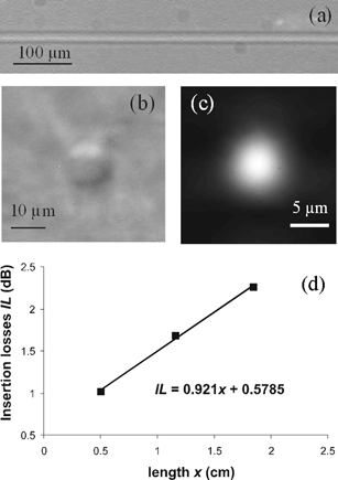 | ||
| Fig. 2 Top (a) and side (b) views of a femtosecond laser fabricated optical waveguide in fused silica; (c) Near field of the fundamental waveguide mode at 543 nm wavelength; (d) measurement of the propagation losses at 543 nm using the cut-back technique. | ||
The performances of the waveguides obtained in plain fused silica substrates appear fully adequate for our present application, in terms of mode profiles and propagation losses.
2.2 On-chip waveguide integration
The next challenge was the integration of the optical waveguides in LOC devices, to enable selective excitation and probing of the content of the microfluidic channels. We used a commercial CE chip (model D8-LIF from LioniX BV). The chip layout is shown in Fig. 3: it consists of two crossing microchannels (folded in a complex way in order to reduce the chip footprint), that are responsible for the sample injection (channel going from reservoir 1 to 3) and for the electrophoretic separation (channel going from reservoir 2 to 4). The separated microfluidic plugs at the end of the channel 2–4 are typically detected by LIF using a confocal microscope. We set out to fabricate, by the femtosecond laser, a series of waveguides perpendicular to the separation channel towards its end (red lines in Fig. 3(a)).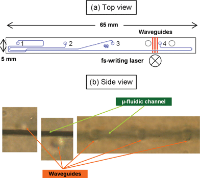 | ||
| Fig. 3 (a) Layout of the CE chip, on which the optical waveguides have been inscribed; (b) side views of femtosecond laser written waveguides at different positions with respect to the microfluidic channel. | ||
The microfluidic channels lie 500 µm below the chip surface and are rather small, with a rectangular cross-section measuring 50 µm in width and 12 µm in height. The positioning of the optical waveguide with respect to the microfluidic channel is thus quite challenging, in particular in the depth direction where the microfluidic channel dimension is smaller. A specific alignment procedure was developed, which exploits the nonlinear absorption to significantly enhance the limited resolution of the 0.3 NA focusing objective. A reference position is taken on the sample surface, opposite to the microscope objective, by looking at the focus position where surface ablation is obtained (revealed by spot degradation of a collinear HeNe laser beam). From this reference position the focus of the writing beam is moved inside the sample by a calibrated distance in order to reach the microchannel region. This very selective and reproducible alignment spoils a negligible part of the sample surface but allows control of the waveguide position with respect to the channel with a precision higher than 2 µm. This allowed the fabrication of waveguides, either tangent to the microfluidic channel, for evanescent sensing, or crossing it for direct excitation. Fig. 3(b) shows several microscope images of the optical waveguides end-view together with the microfluidic channel. From left to right, the position control can be appreciated, with one waveguide slightly above the microfluidic channel, one slightly below and three perfectly centred (in the third image the microfluidic channel is out of focus to allow visualization of the centred optical waveguides).
To prevent damaging of the channel walls when the laser crosses them, the writing beam was interrupted a few µm before the channel and restored just after it, by synchronizing a beam shutter with the driver of the translation stage. Stopping the waveguides a few µm before the channel does not cause any problems since, due to the low numerical aperture of the waveguides, the Rayleigh range of the light coming out of them exceeds 50 µm and thus the excitation remains quite confined when crossing the microfluidic channel. It is also important to note that, despite the fact that the waveguides are written very close to the bonding surface between the two glass slabs of the microfluidic chip, no detectable damage was induced; this indicates that the bonded glass slabs behave as a bulk piece.
These results demonstrate that our direct inscription technique allows the integration of high-quality buried optical waveguides on a functional microfluidic chip. This post-processing capability is unique and provides a very strong design flexibility for the photonic devices to be integrated.
3. Fluorescence detection
In order to demonstrate the capability of the femtosecond laser written optical waveguides to excite fluorescence inside the microfluidic channel, the latter was filled with a solution of Rhodamine 6G (R6G) dissolved in a phosphate buffer (pH 7.2), used as model fluorescent dye. Light at 532 nm from a continuous wave laser (model 4301-010, Uniphase) was coupled into the waveguide via an optical fiber. Fig. 4 shows a microscope image of the yellow fluorescence for an R6G concentration of 10 µM. The excitation is very selective in space (10 µm, as the waveguide diameter), as a further confirmation of the very low leakage out of the waveguide, which is quite important for a high spatial resolution in the CE experiments. In addition, the excited fluorescence covers the whole width (50 µm) of the channel due to the low divergence of the excitation light coming from the waveguide. The results shown in Fig. 4 thus demonstrate the capability of the integrated optical waveguide to excite with high spatial selectivity the contents of the microfluidic channel.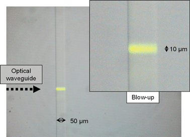 | ||
| Fig. 4 Microscope image of fluorescence from a microfluidic channel in a commercial LOC, filled with R6G, excited by an optical waveguide orthogonal to the channel. The waveguide is not visible due to the low refractive index contrast. A long-pass filter rejects the 532 nm excitation light. | ||
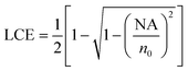
The experimental setup used for the LIF experiments is shown in Fig. 5: it combines compactness, portability, high sensitivity and strong background reduction. The CE chip is inserted in a commercial cartridge providing reservoir connections and electrical contacts (MCC-1 of the Capella platform, CapiliX BV). The fluorescence is collected by an optical fiber pigtailed to the chip in correspondence to the excited portion of the microfluidic channel, in a 90° geometry with respect to the exciting waveguide, thus achieving a strong suppression of the exciting light background. Both the numerical aperture and the diameter of the optical fiber were selected in order to maximize the collected fluorescence and limit the effect of stray light. The light collection efficiency (LCE), defined as the fraction of isotropic fluorescence collected by the optical system, is given by12
| LCE = Ω/4π = 1/2(1 − cosθmax) | (1) |
NA ![[double bond, length as m-dash]](https://www.rsc.org/images/entities/char_e001.gif) n0sinθmax n0sinθmax | (2) |
 | (3) |
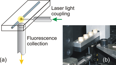 | ||
| Fig. 5 (a) Scheme of the setup used for the LIF experiments, with two optical fibers for fluorescence excitation and collection; (b) picture of the setup, with the microfluidic chip inserted in the cartridge. | ||
For NA = 0.5 we achieve a LCE of 3%, which is comparable to that of a confocal microscope objective, with the advantage of added integration and system portability given by the fiber.
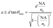
An additional constraint to be satisfied is that the fiber cross section is large enough to intercept all the rays contanined within θmax. Assuming the fluorescence as a point source located at a distance d below the chip surface, and calling a the fiber radius, one obtains
 | (4) |
For the numerical values relevant to our case (d = 500 µm, n0 = 1.45) we obtain a ≥ 180 µm. We used a collection fiber with NA = 0.48 and a core radius of 300 µm (model HWF-H-600T, Ceram Optec), which satisfies both requirements. The fiber has a fused silica core (to minimize autofluorescence) and a polymer cladding to provide high refractive index contrast. We used an optical fiber to collect the fluorescence, rather than a second inscribed waveguide, because: (i) in the present geometry the path from the excited volume to the microchip surface is only 500 µm, therefore a large core area fiber can easily intercept a wide solid angle of the emitted fluorescence; (ii) it is very difficult with any fabrication technology to integrate a waveguide with NA comparable to the fiber we used, thus, notwithstanding the closer collection allowed by a waveguide, a larger amount of fluorescence would have been lost; (iii) a high numerical fiber would have been however necessary to deliver the light collected by the waveguide to the detector. A final comment on the collecting fiber is that its core diameter of 600 µm greatly relaxes the alignment with the microchannel which can be performed by naked eye.
The light collected from the fiber is collimated and refocused by aspherical lenses (focal length f = 20 mm, NA = 0.54) onto a photon counting photomultiplier (PMT, Hamamatsu, model H6240-01, dark counts ≈100 cps). A notch filter (Semrock, model NF01-532U-25) and an interference filter (Corion, model 560-101-6952, 10 nm bandwidth at 560 nm) are placed between the collimation and focusing lenses. The output signals from the PMT are recorded by a 16 bit A/D board (PCI6013, National Instruments) and processed using a program written with LabVIEW (National Instruments).
In order to assess the sensitivity of our system, we performed a LOD measurement. To this purpose the chip was filled with progressively higher concentrations of R6G. Fig. 6 shows the fluorescence as a function of concentration for an average power of 100 µW coupled into the waveguide.
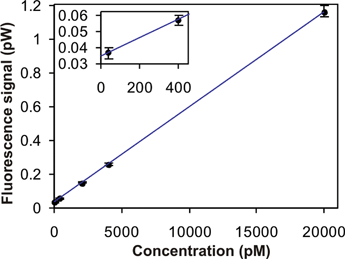 | ||
| Fig. 6 LOD measurement for a microfluidic channel filled with R6G, using a 532 nm excitation wavelength and the detection setup shown in Fig. 5. | ||
The curve displays an excellent linearity and shows the capability of our system to detect very low chromophore concentrations, down to the 40 pM level. This LOD compares very well with values reported in the literature,7 in particular with those obtained using the ‘on-chip’ approach and similar geometries (e.g. lit.,8 250 pM and lit.,12 500 pM). The sensitivity reported here is currently limited by the background signal, measured in a channel filled with buffer and equal to 34 fW (or 10000 cps of the PMT). It is worth noting that the fluorescence signal, corresponding to the lowest concentration we measured, exceeds the background level by an amount which is seven times higher than the corresponding shot noise.
The LOD could be significantly decreased by increasing the excitation power, optimizing the quantum efficiency of the detector and reducing the background signal. The origin of this background is unclear and still under investigation. Rayleigh scattering of the excitation light is expected to be strongly suppressed by the combination of a 90° collection geometry and the notch filter. It may be due to residual autofluorescence or Raman scattering from the fused silica chip substrate; choice of an optimized glass substrate and polishing of the end faces of the glass chip should lead to further background reductions.
4. Conclusions
In this work we have used femtosecond laser writing to fabricate high quality optical waveguides in fused silica LOCs and demonstrated their capability to excite with high spatial selectivity fluorescent molecules flowing in the microfluidic channels. Our approach is quite powerful because it allows the integration of photonic functionalities by simple post-processing of commercial LOCs, fabricated with standard techniques. The integrated excitation/detection scheme discussed here could strongly increase the portability and compactness of the LOCs by overcoming the present limitation where microfluidic systems are coupled to macroscopic bulk optical detection systems.In addition, taking advantage of the three-dimensional capabilities of our technique, more complex functionalities could also be implemented, which are not possible with bulk optics, as multipoint excitation through waveguide splitters or interferometric sensing with an integrated Mach-Zehnder interferometer. We believe that our results may establish a new paradigm for the integration of photonic functionalities into fused silica LOCs.
Acknowledgements
This work was funded by the European Commission, 6th FP STREP Project Contract No. IST-2005-034562 [Hybrid Integrated Biophotonic Sensors Created by Ultrafast laser Systems (HIBISCUS)].References
- R. D. Reyes, D. Iossifidis, P. A. Auroux and A. Manz, Anal. Chem., 2002, 74, 2623–2636 CrossRef CAS.
- P. A. Auroux, D. R. Reyes, D. Iossifidis and A. Manz, Anal. Chem., 2002, 74, 2637–2652 CrossRef CAS.
- G. M. Whitesides, Nature, 2006, 442, 368–373 CrossRef CAS.
- A. J. deMello, Nature, 2006, 442, 394–402 CrossRef CAS.
- P. Yager, T. Edwards, E. Fu, K. Helton, K. Nelson, M. R. Tam and B. H. Weigl, Nature, 2006, 442, 412–418 CrossRef CAS.
- E. Verpoorte, Lab Chip, 2003, 3, 42N–52N RSC.
- B. Kuswandi, J. NurimanHuskens and W. Verboom, Anal. Chim. Acta, 2007, 601, 141–155 CrossRef CAS.
- J. Hubner, K. B. Mogensen, A. M. Jorgensen, P. Friis, P. Telleman and J. P. Kutter, Rev. Sci. Instrum., 2001, 72, 229–234 CrossRef CAS.
- K. B. Mogensen, N. J. Petersen, J. Hübner and J. P. Kutter, Electrophoresis, 2001, 22, 3930–3938 CrossRef CAS.
- K. B. Mogensen, P. Friis, J. Hübner, N. J. Petersen, A. M. Jorgensen, P. Telleman and J. P. Kutter, Opt. Lett., 2001, 26, 716–718 CAS.
- K. B. Mogensen, J. El-Ali, A. Wolff and J. P. Kutter, Appl. Opt., 2003, 42, 4072–4079 CrossRef CAS.
- C. L. Bliss, J. N. McMullin and C. J. Backhouse, Lab Chip, 2007, 7, 1280–1287 RSC.
- D. Yin, D. W. Deamer, H. Schmidt, J. P. Barber and A. R. Hawkins, Opt. Lett., 2006, 31, 2136–2138 CrossRef CAS.
- R. W. Applegate Jr, J. Squier, T. Vestad, J. Oakey, D. W. M. Marr, P. Bado, M. A. Dugan and A. A. Said, Lab Chip, 2006, 6, 422–426 RSC.
- D. Yin, E. J. Lunt, M. I. Rudenko, D. W. Deamer, A. R. Hawkins and H. Schmidt, Lab Chip, 2007, 7, 1171–1175 RSC.
- R. Mazurczyk, J. Vieillard, A. Bouchard, B. Hannes and S. Krawczyka, Sens. Act. B, 2006, 118, 11–19 CrossRef.
- D. Psaltis, S. R. Quake and C. Yang, Nature, 2006, 442, 381–386 CrossRef CAS.
- C. Monat, P. Domachuk and B. J. Eggleton, Nature Photon., 2007, 1, 106–114 Search PubMed.
- K. Itoh, W. Watanabe, S. Nolte and C. Schaffer, MRS Bulletin, 2006, 31, 620–625 CAS.
- R. R. Gatass and E. Mazur, Nature Photon., 2008, 2, 219–225 Search PubMed.
- K. M. Davis, K. Miura, N. Sugimoto and K. Hirao, Opt. Lett., 1996, 21, 1729–1731 CAS.
- R. Osellame, N. Chiodo, G. Della Valle, G. Cerullo, R. Ramponi, P. Laporta, A. Killi, U. Morgner and O. Svelto, J. Sel. Top. Quantum Electron., 2006, 12, 277–285 Search PubMed.
- S. M. Eaton, W. Chen, L. Zhang, H. Zhang, R. Iyer, J. S. Aitchison and P. R. Herman, IEEE Photon. Technol. Lett., 2006, 18, 2174–2176 CrossRef.
- R. Osellame, S. Taccheo, M. Marangoni, R. Ramponi, P. Laporta, D. Polli, S. De Silvestri and G. Cerullo, J. Opt. Soc. Am. B, 2003, 20, 1559–1567 Search PubMed.
- R. Osellame, V. Maselli, R. Martinez Vazquez, R. Ramponi and G. Cerullo, Appl. Phys. Lett., 2007, 90, 231118 CrossRef.
- L. Shah, A. Y. Arai, S. M. Eaton and P. R. Herman, Opt. Express, 2005, 13, 1999–2006 CrossRef.
| This journal is © The Royal Society of Chemistry 2009 |