Potential applications of hierarchical branching nanowires in solar energy conversion
Matthew J.
Bierman
and
Song
Jin
*
Department of Chemistry, University of Wisconsin-Madison, 1101 University Avenue, Madison, Wisconsin, 53706, USA. E-mail: mbierman@chem.wisc.edu; jin@chem.wisc.edu; Web: jin.chem.wisc.edu
First published on 27th July 2009
Abstract
Nanoscience and nanotechnology can provide many benefits to photovoltaic and photoelectrochemical applications by combining novel nanoscale properties with processability and low cost. Taking advantage of high quality, high efficiency, yet low cost nanomaterials could potentially provide the new and transformative approaches to enable the proposed generation-III solar technologies. Nanowires are interesting because they have a long axis to absorb incident sunlight yet with a short radial distance to separate the photogenerated carriers. In this perspective, we further suggest that more “complex” nanostructures, both in the form of hierarchically branching/hyperbranching nanowire structures and in the form of multi-component nanowire heterostructures of diverse materials, are potentially even more interesting for solar energy harvesting and conversion. The common bottom-up synthetic techniques to induce branching in nanowires to form hierarchical nanowire structures are reviewed. Several potential strategies for their incorporation into solar conversion devices are discussed and some fundamental issues and future directions are identified.
 Matthew J. Bierman Matthew J. Bierman | Matthew Bierman received his B.S. from the University of Wisconsin-La Crosse in 2003 and his Ph.D. from the University of Wisconsin-Madison in 2009. His work in nanoscience is motivated by materials development for energy applications including photovoltaics. His thesis work centered on nanowire growth mechanisms, including the introduction of the dislocation-driven nanowire growth mechanism, which was recognized with a 2009 Materials Research Society Graduate Student Award. He will be continuing his energy related research at the California Institute of Technology as a postdoctoral associate. |
 Song Jin Song Jin | Song Jin received his B.S. from Peking University in 1997 and his Ph.D. from Cornell University in 2002. He has been an assistant professor of chemistry at the University of Wisconsin-Madison since 2004. He is interested in the chemistry and physics of nanoscale materials. Dr Jin studies the fundamental formation mechanisms of nanowires, their novel physical properties, and applications in photovoltaic and thermoelectric energy conversion, nanospintronics, and nanomedicine. He has received NSF Career Award and ACS Exxon Mobil Solid State Fellowship, is a Sloan Research Fellow and a Research Corporation Cottrell Scholar, and was recognized as a TR35 by MIT Technology Review magazine in 2006. |
Broader contextSolar energy is clean, renewable, and nearly inexhaustible, and yet is not in widespread use. Solar conversion devices are not yet ubiquitous because of the relatively large cost of energy produced this way when compared to traditional energy sources such as fossil fuels. In order to bring the cost of solar energy in line with other sources, new science and new technology are needed. A variety of materials with at least two nanoscale dimensions (nanomaterials), from nanocrystals to nanowires, nanorods, and nanotubes, have been utilized to harvest solar energy that are cheaper than current technology while remaining efficient or could be even more efficient. Nanowires are interesting because they have a long axis to absorb incident sunlight yet with a short radial distance to collect the photogenerated carriers. We further suggest that hierarchically branching nanowires can be even more beneficial over conventional planar devices than simple nanowire arrays. In this perspective, we summarize the known mechanisms to control nanowire branching, identify the fundamental issues and suggest ways to incorporate them into solar conversion devices. |
1. Challenges of renewable energy and nanowire structures for solar energy conversion
Providing renewable energy without adverse environmental effects is one of, if not the, most important scientific challenge faced by our generation. While conventional fossil fuels can meet our predicted doubling of world energy consumption by mid-century, the impacts of additional atmospheric CO2 and other pollutants must be addressed.1 Solar energy is our largest global renewable energy source, with the potential for providing orders-of-magnitude more energy than will be consumed annually.2 Meeting this demand will require multiple avenues of research, including both photovoltaic (PV) devices to directly generate electricity from sunlight, and photoelectrochemical (PEC) cells to convert solar energy into chemical fuels which can be stored and solves the problem of intermittent solar energy sources and provides portable fuels for transportation uses. If used in water splitting to produce H2, PEC devices could also mitigate the effects of the industrial water–gas shift reaction for H2 production, which is currently one of the world's largest contributors to anthropogenic CO2.The problems with conventional planar junction silicon photovoltaics are well documented. Silicon has an indirect bandgap and is inefficient at absorbing incident light. Therefore, a thickness of 125 µm silicon is required to absorb 90% of incident sunlight, in contrast to 900 nm of GaAs for the same efficiency.3 Because of this large thickness (Fig. 1a), even if a photon is absorbed, collected photocurrent is reduced since the minority carrier diffusion length is limited by various recombination processes within the absorber region. Increasing minority carrier diffusion length requires very pure, high quality, single crystalline silicon, which greatly increases the cost and complexity of functional silicon photovoltaic devices. Polycrystalline and amorphous silicon PV devices have a lower cost of fabrication but suffer in solar conversion efficiency due to the shorter minority carrier diffusion length.4,5 Multi-junction single-crystalline GaAs solar cells can be quite efficient but their materials cost and fabrication cost are very high. A variety of thin film PV devices based on non-silicon materials are inexpensive but their efficiency is not yet competitive with single crystalline silicon.4,5
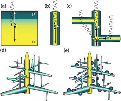 | ||
| Fig. 1 Advantages of vertical nanowires and hyperbranched nanowires over planar solar energy conversion devices. Planar devices (a) must be thick enough to absorb incident light, which places materials quality restrictions due to limited minority carrier diffusion lengths. Nanowires (b) have a long axis to absorb incident light, and orthogonally, a short radial axis to separate charge, accommodating lower quality materials. Introducing branching (c) increases light scattering and therefore photocarrier generation. More complex morphologies such as hyperbranched nanowire heterostructures (d) and nanocrystal-sensitized (or catalyst-decorated) nanowires (e) can also be interesting for solar conversion. | ||
Nanoscience and nanotechnology suggest new ways to solve the performance/cost tradeoff that has limited large-scale commercial applications of solar energy conversion devices. Chemically synthesized nanocrystals, nanowires, nanorods, nanotubes, and a variety of other nanostructures offer new opportunities for solar energy conversion that promise lower fabrication cost and higher conversion efficiency.6 As a result, there has been intensive research worldwide directed at taking advantage of nanomaterials to improve the applications of solar energy conversion. For example, solution grown colloidal semiconductor nanocrystals can be readily spin-coated or blended with semiconducting polymers to allow the facile fabrication of unconventional thin-film solar cells.7–10 Furthermore, the performance of light harvesting materials may actually be enhanced by various nanoscale mechanisms11 such as multiple exciton generation12,13 or the size-dependent control of the absorption wavelength of a quantum-confined particle.14
A variety of semiconductor nanowires can be synthesized in single-crystalline form with precisely controlled structures, diameters, lengths, chemical compositions and doping/electronic properties using a variety of processes such as the nanocluster catalyzed vapour–liquid–solid (VLS) growth mechanism.15 These one-dimensional (1-D) nanowires have great promise in solar energy conversion.16–21 Compared with conventional planar single crystalline or thin film PV or PEC cells (Fig. 1), in a nanowire, the light absorption and carrier separation occur in orthogonal directions (Fig. 1b) so solar light absorption occurs along the longer dimensions of the nanowire (microns or more) while the carrier separation occurs by diffusion across the short radial distance (tens of nanometres).22 As a result, overall device performance does not significantly suffer if lower quality (and less expensive) materials are used. Unconventional semiconductor materials or lower cost synthetic methods that create more defects and impurities might then become tolerable for large-scale solar applications.23 Even if a crystal defect exists within a nanowire, or indeed if an entire nanowire is defective, the performance of the entire device is not impeded as with single crystal devices.
In this perspective, we will build on these ideas and further expand the concept to argue that more “complex” nanostructures, both in the form of hierarchically branching/hyperbranching nanowire structures and in the form of multi-component nanowire heterostructures of diverse materials, are potentially even more interesting for the applications of solar energy harvesting and conversion. We offer a review of the rational synthetic strategies to create such complex nanostructures, and then suggest preliminary ideas and fundamental issues that need to be addressed in order to fully take advantages of such nanostructures for solar energy conversion. The use of nanomaterials, and especially branching nanowires, provides a pathway to reduce materials cost while ideally maintaining the efficiency of the host material, which represents the so-called Generation-III solar technologies24 that combine efficiency with cost.
2. Why hierarchical branching nanostructures matter
Simple chemical synthesis can now readily prepare increasingly complex 3-D hierarchical branching nanowire structures25–30 that further promise to improve the solar energy harvesting from that of simpler 1-D nanowire arrays. The addition of branches to arrays of nanowires (Fig. 1c) improves light harvesting first by adding more material to absorb incident light, and second by intensely scattering light that is not absorbed, resulting in a longer effective path for light to travel through the absorber layer for the same amount of material used in a conventional planar device. Just as trees in the natural world expose large surfaces for effective photosynthesis, these extensively branched structures have large area that harvest solar light and cause increased scattering that improves light absorption. In one example, the added texture of an unaligned forest of simple silicon nanowires already reduced incident light reflectance by one to two orders of magnitude over an equivalent thin film for the entire 300–1100 nm spectrum.20 Just as the fractal geometry of natural trees allow water and carbohydrates, the products of photosynthesis, to be efficiently transported, the dendritic-like semiconductor nanostructures optimizes efficient carrier collection from the numerous terminals to a central trunk. Provided the trunk/branch junction remains epitaxial, there is still a direct carrier collection pathway for photo-excited carriers in the branches as discussed in detail later. The high surface area can also increase the number of interactions between surface catalytic centers in PEC cells. We expect the incorporation of such hierarchical nanostructures into a solar conversion device will be a dramatic departure from the conventional paradigm of planar junction solar cells and will be quite challenging (see Section 5).3. Synthesis and structures of branched and hyperbranched nanowires
These controlled 3-D hierarchical nanowire structures are viable from the “bottom-up” paradigm of nanomaterials growth, but are difficult and expensive, if not impossible, to achieve through conventional “top-down” lithographic fabrication. There have been many demonstrations of nanowire branching in recent literature, but no organization of their relatedness. Here we attempt to summarize the representative approaches to induce branching in nanomaterials to provide a pathway for others. We do not intend this to be a comprehensive overview of all branching nanowires reported but rather illustrative of the basic strategies.3.1 Metal catalyzed nanowire growth with sequential catalyst deposition.
Perhaps the simplest method of nanowire branching involves the sequential deposition of a suitable metal catalyst, followed by vapour–liquid–solid (VLS), solution–liquid–solid (SLS) or other catalyst driven nanowire growth, all of which use metal nanoparticles that can form low-melting point eutectic alloys with the targeted materials to serve as the catalytic seeds for 1-D anisotropic growth.15 In the VLS process, a vapour-phase reactant diffuses into liquid eutectic alloy droplets. Once the droplet becomes supersaturated, it nucleates out a solid nanowire, whose diameter is controlled by the diameter of the catalyst and length by reaction time. This process can be cycled as often as a new generation of branches is desired. Early examples (Fig. 2) include vapour phase synthesis of branched and hyperbranched nanowires of silicon27 and III-V materials including GaN,27GaP,26 and InAs,31,32 as well as tin-doped indium oxide (ITO).33 Sequential SLS growth from solution has also been demonstrated.34 This approach also allows differing catalyst metal, or even catalyst size, to be used for alternate generations of branches, providing additional control. For instance, it is known for silicon nanowires that wire diameter influences growth direction: wires larger than 20 nm grow in a (111) direction, wires smaller than 10 nm grow in a (110) direction, with (112) growth axis wires existing in the intermediate range.35 It has also been demonstrated that catalyst composition controls the growth axis in silicon36 and the growth rate and shape in branches of InAs trees.32 For photoelectrochemical applications, it may be desirable to control or change the growth direction of a nanowire to present (or shield) certain facets because it is well known that certain crystallographic planes have higher catalytic activity than others. Additionally, control of growth direction may be useful to interconnect arrays of freestanding nanowires as shown in Fig. 2c. Controlling the growth direction by choice of catalyst provides one such additional control over nanostructures that can be tailored for individual applications.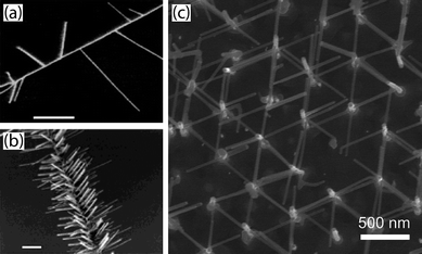 | ||
| Fig. 2 Nanowire branching from sequential addition of VLS catalysts. Sequential catalyst application can be used to control branch density as shown with Si nanowires (a,b).27 Scale bars are 1 µm. This technique can be used to create an array of interconnected nanowires (c) by connecting patterned vertically aligned nanowires as shown in this plan-view electron micrograph.31 Images reproduced with permission ACS. | ||
This approach can also be adapted to integrate different materials into trunk/branch heterostructures. A clear example has been the growth of CdS branches grown sequentially from a ZnS trunk.37 After the second application of gold catalysts, the precursor was changed from cadmium dithiocarbamate to zinc dithiocarbamate. ZnO branches can also be grown from an In2O3 trunk.38 Another interesting heterojunction branching example is in the case of carbon nanotubes grown only from the tip of a SiC micropost, creating the world's smallest brush.39
3.2 In situ VLS catalyst generation to induce hyperbranching
Sequential seeding to induce branching in nanowires requires opening the synthesis chamber between additional generations of nanowire growth. In addition to being a cumbersome process, the previously grown nanowires could be oxidized. This can compromise the epitaxial relationship between trunk/branch nanowires that could prove detrimental to applications.The continuous in situ generation of a VLS catalyst during nanowire growth provides the source for multiple generations of branches to nucleate and grow at the same time (Fig. 3). This allows the growth of very dense hierarchical branched nanowire networks that have high quality epitaxial junctions, termed “hyperbranching”. The term “hyperbranched” can be perhaps traced back to the terminology in polymer literature, where “hyperbranched polymers” refer to non-linear polymers that have many branches and possibly many generations of branches. This is in contrast to “dendritic polymers” or “dendrimers”, which have the same number of branches at each branching point. Several recent studies have involved materials systems capable of the in situ formation of a catalyst.29,40–43 In the case of PbS (PbSe), lead metal itself serves as an in situ generated catalyst from the PbCl2 source formed in a reducing H2 atmosphere and can be rationalized from the Pb-S (Pb-Se) phase diagram. As shown in Fig. 3, the continuous introduction of catalyst randomly on the surface nucleates a dense, orthogonal network of nanowires and generates multiple generations of branches for as long as additional precursor is added. An analogous process could have been observed in the solution-phase synthesis of PbSe nanowires.44 Branching of PbSe nanowires was observed as the Pb : Se ratio approached 4 : 1. This lead-rich synthesis allowed Pb catalysts to condense on the growing PbSe nanowire, nucleating new branches at a right angle.
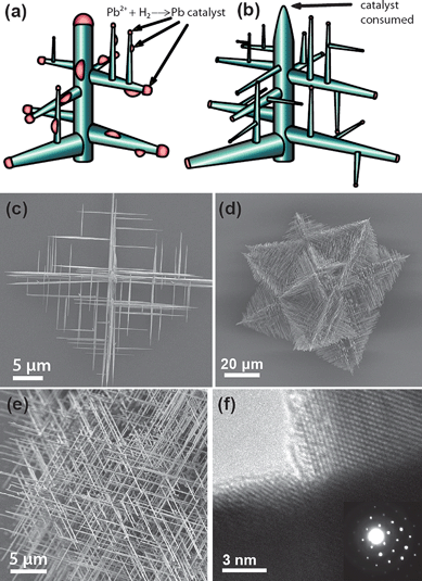 | ||
| Fig. 3 Hyperbranching nanowires through continuous in situcatalyst generation. Nanowires grow randomly with one generation growing epitaxially from previous generations (a), until a dense hyperbranched nanowire network is produced (b). This can be seen in nanowires of the cubic PbS and PbSe system (c, d, e) where lead metal self-catalyzes the nanowire growth.29Transmission electron microscopy (f) shows that the branches remain epitaxial. Images reproduced with permission ACS. | ||
The above examples of in situ catalysis are materials systems capable of self-catalytic VLS45 which most often have a low melting metal as one of the elements of the binary compounds, as in the case of the Ga-metal catalysis of GaN46 and the Pb-metal catalysis of PbS,28,29 but the catalyst material need not be self-similar as in the case of PbSe grown with In, Ga, or Bi40,47 or of InAs nanowires catalyzed by an additional Mn source.48 When the catalysts can be continuously fed into the reaction system, multiple generations of nanowire growth can possibly occur.
3.3 Combinations of screw dislocation driven and VLS growth mechanism
Combining various nanowire growth mechanisms is one pathway to gain additional control over the resulting nanowire hierarchy. A prominent example of this are “pine-tree” like nanowires of PbS (Fig. 4a,d) we recently reported.28 Through these curious structures, we discovered a fundamentally different nanowire growth mechanism that is driven by axial screw dislocations (Fig. 4b,c). In this growth process, the self-perpetuating surface steps of screw dislocations provide the facile spiral growth fronts when the supersaturation is lower than what is required for the layer-by-layer crystal growth on perfect crystal facets (such as VLS) and drive the 1-D anisotropic crystal growth of nanowires without catalysts.28 The cone-shaped nano “pine-trees” are the result of simultaneous fast dislocation-driven trunk nanowire growth and the slower VLS driven branch growth while the helical rotation of the branches are the consequence of the strain of the axial dislocation called “Eshelby twist”. This approach is a fundamental advance to the rational design and synthesis of 1-D nanomaterials because dislocation-driven growth is underappreciated in modern literature on 1-D nanomaterials. It is likely a general method applicable to many materials that are prone to have screw dislocation issues, such as ZnO, GaN, InN, SiC, both in the vapour phase and solution phase synthesis. We have already confirmed that solution grown ZnO nanowires and nanotubes can be driven by screw dislocations.49 For the purpose of producing hierarchical nanostructures, in order to enable simultaneous operations of both dislocation-driven and VLS growth mechanisms, the supersaturation must be in a range where both layer-by-layer growth and dislocation-driven growth coexist.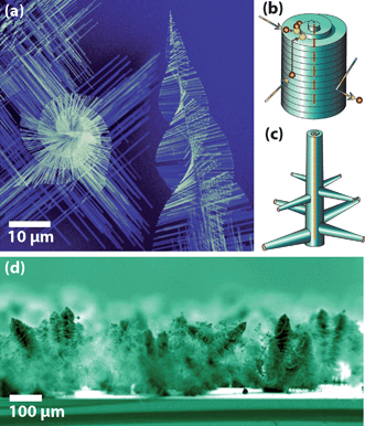 | ||
| Fig. 4 “Pine tree” nanowires of PbS (a) due to the combination of two nanowire growth mechanisms. Screw dislocation driven nanowire growth of the trunk nanowire (b) combined with branch VLS driven growth (c) combine to produce this morphology. Upright PbS pine tree nanowire forests grow on silicon substrates (d).28 Images reproduced with permission AAAS. | ||
3.4 Nanowire tetrapods—zinc-blende/wurtzite stacking faults
Branching has been observed without the addition of intentional branching catalysts in solution-grown nanocrystals or nanorods/nanowires.25,50,51 These nanostructures are made of wurtzite materials, such as CdSe (Fig. 5a),52 that have another cubic-close-packed zinc blende polymorph with very similar thermodynamic stability to its hexagonal-close-packed wurtzite form. They also have a relatively small stacking fault energy to convert between the zinc-blende and wurtzite crystal structures with equivalent growth directions of zinc-blende <111> or wurtzite <0001> and epitaxial match at the interface (Fig. 5b). The nanocrystals first nucleate with a tetrahedral zinc-blende core because zinc blende structure is more favored at smaller nanoscale size. When the tetrahedron core reaches a certain critical size, branched nanowires with two, three, or up to four equivalent wurtzite branches nucleate and grow from its four equivalent <111> directions resulting in a tetrapod geometry, because wurtzite is the more stable structure in bulk. This strategy has been used to create even more complex branching patterns that begin to form a fractal pattern with multiple zinc-blende core areas along a “central” wire.25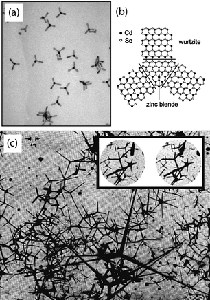 | ||
| Fig. 5 Tetrapods of CdSe52 (a) and the formation mechanism of these and other tetrapods50 (b) with zinc-blende/wurtzite polymorphs. Electron micrographs (c) of the original ZnO tetrapods,54 called “fourlings.” Magnification is 40 k×. Inset magnification is 3500×.53 Images reproduced with permission ACS and AIP. | ||
Similar ZnO tetrapods, called “fourlings,” have been produced in the vapour phase (Fig. 5c) by combusting zinc in an oxygen atmosphere, as early as 1944.53,54 Their formation mechanism is similar to CdSe and involves a stacking fault between the central nucleus and each branch. It was originally suggested that a non-classical nucleation of a polycrystalline ZnO nucleus was the source of twinning, and was thought to be the fourling formation mechanism.54 The state of transmission electron microscopy then probably did not allow for lattice imaging and this growth is now thought to involve zinc-blende/wurtzite stacking faults.
So far, materials that form branched structures due to such polymorph instability are mostly confined to zinc blende/wurtzite structural types, but if multiple polymorphs could co-exist with similar stability, analogous behaviours could also occur in other material systems with other structural types and produce branching geometry different from tetrapods. One related example has been demonstrated in PbSe “merged-y” nanowires, where a twin plane in a [110] growth direction nanowire splits into two branching nanowires growing in <100> directions.44
3.5 Dendritic crystal growth (Diffusion limited aggregation; DLA)
Strictly speaking, the growth of dendritic crystals is not a method to induce branching in nanowires. Based on classical crystal growth theory,55 dislocation (spiral) growth, layer-by-layer growth (which encompasses the metal-catalyzed VLS or SLS growth), and dendritic growth require progressively higher and distinctively different supersaturation regimes. The high concentrations needed for true dendritic crystal growth are outside the range of supersaturation required by nanowire growth.55 However, when carefully controlled, dendritic growth of crystals do provide pathways to synthesize highly hierarchical (and/or fractal) nanostructures56 with one central collection pathway back to the underlying substrate, and could potentially be used in solar energy conversion applications as in the case of Fe2O3 “nanocauliflower” crystals.57 We further suspect that many of the reported “nanoflowers” and other complex morphologies commonly seen in the contemporary nanomaterials literature could have been synthesized in this crystal growth regime. The crystallinity and materials quality might not be as good as single-crystal epitaxial branched nanowires carefully grown in lower supersaturation regime as the higher growth rate results in high defect density and many grain boundaries which may impede device performance.3.6 Other branching mechanisms
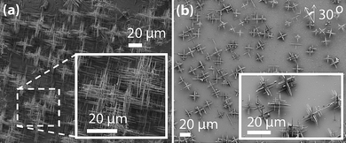
Many other materials systems can show branching or hyperbranching, but the mechanisms are often not completely understood.58,59 One example from our lab is the branching and hyperbranching transition metal-silicide nanowires shown in Fig. 6. The growth of most silicide nanowires using CVD of single source molecular precursors60,61 or chemical vapour transport (CVT)62,63 of silicide solids are not completely understood yet. We suspect that metals could act as catalysts for silicon nanowires, which are then alloyed with additional metal vapour to form a silicide.64 The silicide nanowires can be grown off of Si nanowires that have been previously synthesized (Fig. 6c) to produce brush like nanostructures. The FeSi nanowires synthesized viachemical vapour transport are hyperbranched65 (Fig. 6a,b) and the mechanism for such branching are not understood. Many silicides exhibit multiple phases,66 making these systems rich with possibilities, such as branching higher-manganese silicides nanowires (Fig. 6d). A different mechanism has been proposed for another silicide, TiSi2, that results from the chlorine stabilization of certain crystal facets leading to preferential nanowire branching that creates a “nano-net” morphology.67 The variety of crystal structures and compositions possible for silicides materials give their nanostructures potential to exhibit a rich diversity of behaviours. The potential for many other material families to yield hierarchical nanowire structures are likely not fully exploited.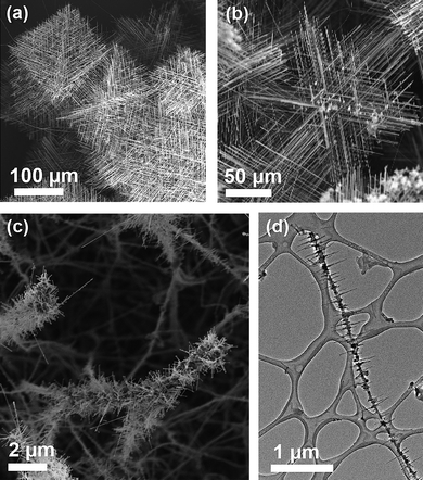 | ||
| Fig. 6 Branching and hyperbranching in transition metal silicides nanowires. Hyperbranched FeSi nanowires synthesized viachemical vapour transport (a,b). FeSi nanowires growing off of a Si nanowire core (c), and the higher manganese silicides branching nanowires (d). | ||
4. Advantages of nanowire heterostructures as complex multi-component nanostructures
Another advantage of nanomaterials is that epitaxial crystal growth between dissimilar materials becomes feasible in nanostructures because the nanoscale dimensions relax lattice-matching requirements and allow the creation of high quality, defect-free epitaxial junctions that would be impossible in bulk films.68,69 These lattice matches are not limited to materials with similar lattice parameters or even with the same structure types. As long as the 2-D translational symmetry on both side of the interface allow a common supercell with reasonably good precision and small area,68,70 it is theoretically possible to have heteroepitaxial aligned nanowire growth. For example, a range of III–V semiconductor materials (GaP, GaAs, InAs, InP) form axial nanowire heterostructures71–73 not previously observed in epitaxial thin films. Moreover, well-aligned vertical nanowires that are epitaxial to the underlying crystalline substrate require lattice matches.74,75 Many III–V semiconductor nanowires grow heteroepitaxially on significantly lattice-mismatched (up to 11%) Si76 and Ge77 substrates when the diameters of the nanowires are small. Therefore, a more diverse and unconventional set of materials becomes available for constructing multi-component nanostructures for solar energy harvesting and conversion. Many of these materials combinations would not have been evaluated by previous bulk/thin film literature and should be considered.Nanowire arrays aligned on a substrate are interesting for PV and PEC device applications as seen in the preliminary demonstrations of nanowire solar conversion devices. The greater possibility of heteroepitaxy discussed above presents more options in integrating nanowires into functional devices. Taking the example of PbQ nanowires that are grown in our lab, the [100] directions of the (100) surface (a faces) of rocksalt PbSe can match the [100] direction on the (001) surface (c face) of tetragonal rutile TiO2 with a supercell of 1.84 Å and only 0.03% mismatch (4 × TiO2c = 3 × PbSea). Similarly, the atomic spacing along the [110] direction on the (001) surface of rutile TiO2 (6.495 Å) are identical within 5% of the spacing along the [100] surface of PbSe (6.126 Å). Such benefits are confirmed by our preliminary success in epitaxial growth of PbS nanowires on single crystalline rutile TiO2,30 a wide bandgap semiconductor. Because of the interfacial strain relaxation, more complicated epitaxial relationships on unconventional substrates are allowed as shown in the epitaxial growth of hierarchical PbS nanowires on single crystal NaCl and mica (Fig. 7).30 This approach may allow more efficient charge transfer between absorber/host than, for instance, quantum dot sensitized solar cells coupled with an organic linker.10,78
 | ||
| Fig. 7 Epitaxial growth of hyperbranched nanowires of PbS on (a) single crystalline NaCl, and (b) mica.30 Images reproduced with permission RSC. | ||
Besides the epitaxial nanowires on substrates, many types of unconventional heteroepitaxy have been realized in the nanowire geometry,79 for example, axial heterojunctions,69,71,72 core-shell nanowires,80 or quantum dots decorated nanowires. Some potential approaches to exploit nanowire heterostructures for solar conversion devices are using different materials for axial heterostructures, core/shell (see Fig. 1c) or trunk/branch nanowires (see Fig. 1d and e). Photovoltaic cell designs such as the dye-sensitized solar cells utilize narrow gap (molecular) light absorbers to produce photocarriers that are coupled to a wide bandgap collector material that transports one photocarrier back to the electrode. The idea of sequential branching can be used to couple narrow bandgap absorber branches to a wide bandgap collector trunk nanowire or substrate that would provide an efficient photocarrier collection pathway as illustrated in Fig. 8. Perhaps even several absorber materials with progressively smaller bandgaps can be used to more efficiently harvest the energy from the solar spectrum, akin to the multi-junction solar cells. In fact, due to the quantum confinement and the modification of bandgap, this may be even possible to realize using the same materials system with well controlled nanoscale dimensions.
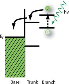 | ||
| Fig. 8 Branched nanowire heterostructures with well controlled electronic structures can improve solar energy harvesting. A narrow bandgap absorber that is matched to the solar spectrum is attached to a wide bandgap transport material like TiO2 to efficiently transport photocarriers to the collector base. | ||
The integration of multiple materials into one nanostructure is potentially significant. Can we seamlessly control diverse materials under continuous synthesis and catalysis conditions? Can we integrate and optimize several materials into a functional PV or PEC cell? Especially for PEC devices such as those for water splitting, several different materials are needed in one integrated functional device, including semiconductor(s) of different bandgaps and dopings, oxygen evolving and hydrogen evolving catalyst materials, all arranged in a nanoscale environment. This in fact mimics the natural photosynthetic systems which are remarkably engineered assemblies of nanostructures. Moreover, the materials involved must meet the different (and sometimes conflicting) requirements of electronic structures, materials compatibility, and chemical stability. For example, to create water compatible devices, many oxide semiconductors such as TiO2 and Fe2O3 with excellent stability are important to explore. Exploring these ideas to create “compositionally complex” multi-component nanostructures from the bottom-up will enable more sophisticated solar conversion device designs that are built on a new paradigm of bottom-up nanotechnology.
5. Challenges in applications of branched nanostructures and fundamental tasks ahead
Employing the hierarchically branching nanowire materials above may be ideal to solving some current solar energy materials problems. In fact, the advantages of hierarchical nanostructures for solar energy harvesting as discussed in this perspective have been preliminarily demonstrated by some early reports. Efficiency enhancement in PV devices of tetrapods and hyperbranched CdSe nanorods blended with conducting polymers has been preliminarily observed and the benefits due to branching were discussed.81,82 It was also commented that the hierarchical nanostructures of the “nano-cauliflower” Fe2O3 photoelectrode were beneficial to the high photocatalytic efficiencies observed.57,83 To fully take advantages of these benefits, we also need to think critically about new, creative ways to utilize the bottom-up synthesized nanowires and other hierarchical nanostructures. Several works have shown the integration of nanowire array electrodes into large area solar conversion devices, preliminarily demonstrating this capability.17,18 More strategies need to be developed. Several suggestions, caveats, and some fundamental scientific issues that need to be addressed are discussed here.With many options to induce branching or hyperbranching in materials systems relevant to solar energy conversion, how do we best take advantage of these complex nanostructures? By incorporating hyperbranched nanowire materials into a photovoltaic cell, light absorption (and therefore cell efficiency) will be increased, while decreasing amounts of material compared to thin film designs could mean cost remains lower than in bulk photovoltaic cells. We suspect that the incorporation of such hierarchical nanostructures into a solar conversion device will be a dramatic departure from the conventional paradigm of planar junction solar cells and will be quite challenging. As a starter, making good electrical contact to the distributed 3-D structures can be a challenge. New paradigms are needed to take advantage of these novel structures for solar energy conversion, and we need to explore various unconventional device designs. We might imagine that for photovoltaic devices liquid junction electrochemical (regenerative) photovoltaic cells could be a promising approach. Suitable redox pairs have to be chosen based on the materials and band alignments to shuttle the holes (or electrons). Inorganic solution-deposited thin film hybrids with hierarchical nanostructures, and nanowire/organic-semiconductor composites might be interesting as well, since the deposition of one of the two active materials is conformal, thus allowing electrical integration with these 3-D structures. The initial practical demonstration of a hyperbranching nanowire photovoltaic cell will likely be a solution or polymer hybrid, or an excitonic solar cell with an active light absorbing dye or quantum dot, as illustrated schematically in Fig. 1e. Comparison to these types of cells sets a practical target for a successful demonstration of a hyperbranching effect, when compared with current cell efficiencies which range from 1.7–1.8% in P3HT/CdSe nanowire hybrid cells,8,81 4.2% in POHT/GaAs thin film hybrid cells,84 or 4.4% for axial heterojunction silicon nanowire cells.85
Enhanced solar energy harvesting due to hierarchical nanostructures applies to both photovoltaic applications where the electrons and holes are collected by electrodes and in solar fuel applications where the electrons and holes carry out redox reactions at catalytic centers. In fact, one may argue that chemically synthesized nanostructures, especially the hyperbranched nanostructures discussed in this perspective, might be intrinsically more suitable for photoelectrocatalysis (such as water-splitting) as opposed to photovoltaic application, because solar fuel production does not require a second solid-phase electrical contact but benefits from the high surface area characteristics of chemically synthesized nanostructures. Because of the high surface area, care must be taken to passivate the material surface for PV applications to prevent excess carrier recombination at nanostructured electrodes. Because of this consideration, perhaps branched nanowire materials could be better suited for use as nanostructured electrodes in a photoelectrochemical cell, effectively turning a limitation in a PV cell into a benefit in a PEC cell.
The high surface area-to-volume ratio of nanostructures is often deleterious because it could cause carrier recombination that reduces performance and creates irreproducibility in device functions.86,87 At the same time, it provides an opportunity to effectively control the electronic processes in nanostructures through passivation or partial passivation. For instance, perhaps trunk nanowires can be passivated to protect current flow while branch nanowires remain exposed and catalytically active (see Fig. 1d).
We need to learn how to make hierarchical nanowire structures more efficiently and controllably. With the understanding of the growth mechanisms, we need to develop conditions for inducing certain degrees of branching to optimize the performance/cost tradeoff. Or we may be interested in a more regular spacing of branches. This is especially true of synthetic schemes that introduce catalysts continuously or that employ conditions to promote the in situ generation of metal catalysts (such as the flow of hydrogen gas in the case of CVD PbS nanowire synthesis). How much control can we have over in situ mechanisms? Also, the conditions necessary for combining distinct modes of nanowire growth (like those combining dislocation-driven and vapour–liquid–solid growth, producing “pine-tree” PbS nanowires) need to be fully investigated88 and possibly expanded to other materials systems to allow greater control of these mechanisms and to create more complex nanostructures.
We also note that careful control over the quality of trunk/branch junctions is critical to maintain the benefits of induced branching. If care is taken to ensure an epitaxial relation between trunk/branch junctions, there remains a continuous “fractal” carrier collection pathway to ensure that all photocarriers are collected by the device instead of recombining at the material's junctions. Perhaps this favors in situ catalysis where the growth atmosphere is never compromised. However, ballistic transport has recently been demonstrated around the trunk/branch junction in InAs branched nanowires grown from sequential nucleation,89 suggesting carriers will not be impeded from the addition of branches. Even more fundamentally, we need to understand the (possibly coherent) carrier separation at nanoscale junctions and the carrier transport through the hyperbranched or dendritic nanowire structures.
There are also other economic and practical considerations. Even though IV–VI and II–VI semiconductors commonly studied so far are nice model nanostructures for fundamental investigations, their practical applications will likely be limited due to toxicity, materials abundance, and photocorrosion. Many other less commonly studied semiconductor materials made of earth abundant elements and environmentally sustainable materials, such as Cu2S, Cu2O, or FeS2,90 may prove much more important in the long term when solar energy conversion technologies is widely adapted on a much larger scale than the current niche applications. For example, some inexpensive metal oxide materials such as Fe2O3 are stable against photo-oxidation in water and are particularly attractive for aqueous photocatalysis.91–93 While some of these generally less explored materials were previously considered to be “poor” semiconductors whose carrier density, mobility, and minority carrier diffusion length were too small to be useful for solar energy applications, they are now much more attractive9,83 because the new device design concepts based on nanowire structures may circumvent the problems. Another practical consideration is that if high temperature reactions are used to synthesize nanowires, there will be some constraints placed on compatible substrates. This can be helped by transferring the as-grown nanowires to other (perhaps unconventional) substrates.94,95 Alternatively, lower temperature solution synthesis pathways, such as the aqueous solution synthesis of ZnO and TiO2nanowires, should also be explored.6,96–98 In fact, the latter will also be less expensive and more amenable to scale up.
6. Summary and outlook
Hierarchically branched and hyperbranched nanowire materials and their heterostructures with diverse chemical compositions can be exploited for enhanced solar conversion efficiencies in photovoltaic and photoelectrochemical devices. In this perspective, we have reviewed the common techniques to induce branching in nanowires, ranging from the sequential application of catalyst particles to the continuous, in situ generation of catalysts for hyperbranching nanowire scaffolds, to combining dislocation-driven with catalyst driven growth. Applying these mechanisms or combinations of mechanisms to nanowire growth enables the formation of trunk/branch structures of the same material, or heterostructures with two or even more complementary materials. These approaches add to the nanowire synthesis toolbox, creating structures from the “bottom-up” paradigm of materials synthesis that are impossible to achieve from a “top-down” approach.We suggest these techniques and the hierarchical nanowire structures will be central to the development of Generation-III solar materials that decrease the cost constraints of bulk, high quality materials while providing pathways for a more efficient conversion and collection of photocarriers. Several potential strategies for their successful incorporation into photovoltaic or photoelectrochemical solar conversion devices are discussed and some fundamental issues and future directions that need attention for furthering the applications of hierarchical nanostructures for better solar conversion devices are identified. It is also possible that the right applications that best utilize these hierarchical nanowire materials have not been discovered, and we may need to depart dramatically from our current paradigm of solar energy technologies to take full advantage of these novel materials. However, we are optimistic that sustained and dedicated research efforts in this promising area would provide us potentially transformative approach to solar energy conversion that is based on nanoscience and nanotechnology.
Acknowledgements
S. J. thanks the NSF (CAREER DMR-0548232), the Sloan Research Fellowship, the Research Corporation Cottrell Scholar Award, DuPont Young Professor Grant, and Exxon Mobil Solid State Chemistry Fellowship for support. We thank our co-workers for the experimental works discussed in this perspective. We also thank Prof. John C. Wright, Prof. Robert J. Hamers, and Prof. Nathan S. Lewis for helpful discussions.References
- N. S. Lewis and D. G. Nocera, Proc. Natl. Acad. Sci. U. S. A., 2006, 103, 15729–15735 CrossRef CAS.
- M. I. Hoffert, K. Caldeira, A. K. Jain, E. F. Haites, L. D. D. Harvey, S. D. Potter, M. E. Schlesinger, S. H. Schneider, R. G. Watts, T. M. L. Wigley and D. J. Wuebbles, Nature, 1998, 395, 881–884 CrossRef CAS.
- J. Singh, Electronics and Optoelectronic Properties of Nanostructures, Cambridge Unversity Press, 2003 Search PubMed.
- A. Shah, P. Torres, R. Tscharner, N. Wyrsch and H. Keppner, Science, 1999, 285, 692–698 CrossRef CAS.
- T. Surek, J. Cryst. Growth, 2005, 275, 292–304 CrossRef CAS.
- I. Gonzalez-Valls and M. Lira-Cantu, Energy Environ. Sci., 2009, 2, 19–34 RSC.
- D. J. Milliron, I. Gur and A. P. Alivisatos, MRS Bull., 2005, 30, 41–44 CAS.
- W. U. Huynh, J. J. Dittmer and A. P. Alivisatos, Science, 2002, 295, 2425–2427 CrossRef CAS.
- Y. Wu, C. Wadia, W. L. Ma, B. Sadtler and A. P. Alivisatos, Nano Lett., 2008, 8, 2551–2555 CrossRef CAS.
- P. V. Kamat, J. Phys. Chem. C, 2008, 112, 18737–18753 CAS.
- A. J. Nozik, Annu. Rev. Phys. Chem., 2001, 52, 193–231 CrossRef CAS.
- R. D. Schaller and V. I. Klimov, Phys. Rev. Lett., 2004, 92, 186601–186601 CrossRef CAS.
- R. J. Ellingson, M. C. Beard, J. C. Johnson, P. Yu, O. I. Micic, A. J. Nozik, A. Shabaev and A. L. Efros, Nano Lett., 2005, 5, 865–871 CrossRef CAS.
- C. B. Murray, C. R. Kagan and M. G. Bawendi, Annu. Rev. Mater. Sci., 2000, 30, 545–610 CrossRef CAS.
- Y. Xia, P. Yang, Y. Sun, Y. Wu, B. Mayers, B. Gates, Y. Yin, F. Kim and H. Yan, Adv. Mater., 2003, 15, 353–389 CrossRef CAS.
- B. Z. Tian, X. L. Zheng, T. J. Kempa, Y. Fang, N. F. Yu, G. H. Yu, J. L. Huang and C. M. Lieber, Nature, 2007, 449, 885–889 CrossRef CAS.
- J. R. Maiolo, B. M. Kayes, M. A. Filler, M. C. Putnam, M. D. Kelzenberg, H. A. Atwater and N. S. Lewis, J. Am. Chem. Soc., 2007, 129, 12346–12347 CrossRef.
- A. P. Goodey, S. M. Eichfeld, K. K. Lew, J. M. Redwing and T. E. Mallouk, J. Am. Chem. Soc., 2007, 129, 12344–12345 CrossRef CAS.
- M. D. Kelzenberg, D. B. Turner-Evans, B. M. Kayes, M. A. Filler, M. C. Putnam, N. S. Lewis and H. A. Atwater, Nano Lett., 2008, 8, 710–714 CrossRef CAS.
- L. Tsakalakos, J. Balch, J. Fronheiser, B. A. Korevaar, O. Sulima and J. Rand, Appl. Phys. Lett., 2007, 91, 233117 CrossRef.
- E. C. Garnett and P. D. Yang, J. Am. Chem. Soc., 2008, 130, 9224–9225 CrossRef CAS.
- B. M. Kayes, H. A. Atwater and N. S. Lewis, J. Appl. Phys., 2005, 97, 114302 CrossRef.
- N. S. Lewis, Science, 2007, 315, 798–801 CrossRef CAS.
- M. A. Green, Third Generation Photovoltaics: Advanced Solar Energy Conversion, Springer-Verlag, Berlin, 2003 Search PubMed.
- D. J. Milliron, S. M. Hughes, Y. Cui, L. Manna, J. B. Li, L. W. Wang and A. P. Alivisatos, Nature, 2004, 430, 190–195 CrossRef CAS.
- K. A. Dick, K. Deppert, M. W. Larsson, T. Martensson, W. Seifert, L. R. Wallenberg and L. Samuelson, Nat. Mater., 2004, 3, 380–384 CrossRef CAS.
- D. Wang, F. Qian, C. Yang, Z. H. Zhong and C. M. Lieber, Nano Lett., 2004, 4, 871–874 CrossRef CAS.
- M. J. Bierman, Y. K. A. Lau, A. V. Kvit, A. L. Schmitt and S. Jin, Science, 2008, 320, 1060–1063 CrossRef CAS.
- M. J. Bierman, Y. K. A. Lau and S. Jin, Nano Lett., 2007, 7, 2907–2912 CrossRef CAS.
- Y. K. A. Lau, D. J. Chernak, M. J. Bierman and S. Jin, J. Mater. Chem., 2009, 19, 934–940 RSC.
- K. A. Dick, K. Deppert, L. S. Karlsson, W. Seifert, L. R. Wallenberg and L. Samuelson, Nano Lett., 2006, 6, 2842–2847 CrossRef CAS.
- K. A. Dick, Z. Geretovszky, A. Mikkelsen, L. S. Karlsson, E. Lundgren, J. O. Malm, J. N. Andersen, L. Samuelson, W. Seifert, B. A. Wacaser and K. Deppert, Nanotechnology, 2006, 17, 1344–1350 CrossRef CAS.
- Q. Wan, M. Wei, D. Zhi, J. L. MacManus-Driscoll and M. G. Blamire, Adv. Mater., 2006, 18, 234–238 CrossRef CAS.
- A. Dong, R. Tang and W. E. Buhro, J. Am. Chem. Soc., 2007, 129, 12254–12262 CrossRef CAS.
- Y. Wu, Y. Cui, L. Huynh, C. J. Barrelet, D. C. Bell and C. M. Lieber, Nano Lett., 2004, 4, 433–436 CrossRef CAS.
- J. L. Lensch-Falk, E. R. Hemesath, D. E. Perea and L. J. Lauhon, J. Mater. Chem., 2009, 19, 849–857 RSC.
- Y. Jung, D. K. Ko and R. Agarwal, Nano Lett., 2007, 7, 264–268 CrossRef CAS.
- J. Y. Lao, J. G. Wen and Z. F. Ren, Nano Lett., 2002, 2, 1287–1291 CrossRef CAS.
- A. Y. Cao, V. P. Veedu, X. S. Li, Z. L. Yao, M. N. Ghasemi-Nejhad and P. M. Ajayan, Nat. Mater., 2005, 4, 540–545 CrossRef CAS.
- J. Zhu, H. L. Peng, C. K. Chan, K. Jarausch, X. F. Zhang and Y. Cui, Nano Lett., 2007, 7, 1095–1099 CrossRef CAS.
- M. Fardy, A. I. Hochbaum, J. Goldberger, M. M. Zhang and P. D. Yang, Adv. Mater., 2007, 19, 3047–3051 CrossRef CAS.
- Y. Chen, L. Campbell and W. L. Zhou, J. Cryst. Growth, 2004, 270, 505–510 CrossRef CAS.
- H. J. Fan, R. Scholz, F. M. Kolb and M. Zacharias, Appl. Phys. Lett., 2004, 85, 4142–4144 CrossRef CAS.
- K. L. Hull, J. W. Grebinski, T. H. Kosel and M. Kuno, Chem. Mater., 2005, 17, 4416–4425 CrossRef CAS.
- M. Law, J. Goldberger and P. D. Yang, Annu. Rev. Mater. Res., 2004, 34, 83–122 CrossRef CAS.
- M. He, P. Zhou, S. N. Mohammad, G. L. Harris, J. B. Halpern, R. Jacobs, W. L. Sarney and L. Salamanca-Riba, J. Cryst. Growth, 2001, 231, 357–365 CrossRef CAS.
- J. Zhu, H. L. Peng, A. F. Marshall, D. M. Barnett, W. D. Nix and Y. Cui, Nature Nanotechnol., 2008, 3, 477–481 Search PubMed.
- S. J. May, J. G. Zheng, B. W. Wessels and L. J. Lauhon, Adv. Mater., 2005, 17, 598–602 CrossRef CAS.
- S. A. Morin, M. J. Bierman, and S. Jin, to be submitted.
- L. Manna, E. C. Scher and A. P. Alivisatos, J. Am. Chem. Soc., 2000, 122, 12700–12706 CrossRef CAS.
- J. W. Grebinski, K. L. Hull, J. Zhang, T. H. Kosel and M. Kuno, Chem. Mater., 2004, 16, 5260–5272 CrossRef CAS.
- L. Manna, D. J. Milliron, A. Meisel, E. C. Scher and A. P. Alivisatos, Nat. Mater., 2003, 2, 382–385 CrossRef CAS.
- M. L. Fuller, J. Appl. Phys., 1944, 15, 164–170 CrossRef CAS.
- G. W. Sears, R. Powell and B. Donn, J. Chem. Phys., 1963, 39, 2248–2251 CrossRef CAS.
- I. V. Markov, Crystal growth for beginners: fundamentals of nucleation, crystal growth and epitaxy, World Scientific, New Jersey, 1995 Search PubMed.
- P. Meakin, Phys. Rep., 1993, 235, 189–289 CrossRef CAS.
- I. Cesar, K. Sivula, A. Kay, R. Zboril and M. Graetzel, J. Phys. Chem. C, 2009, 113, 772–782 CrossRef CAS.
- D. F. Zhang, L. D. Sun, C. J. Jia, Z. G. Yan, L. P. You and C. H. Yan, J. Am. Chem. Soc., 2005, 127, 13492–13493 CrossRef CAS.
- Y. G. Li, B. Tan and Y. Y. Wu, Chem. Mater., 2008, 20, 567–576 CrossRef CAS.
- A. L. Schmitt, M. J. Bierman, D. Schmeisser, F. J. Himpsel and S. Jin, Nano Lett., 2006, 6, 1617–1621 CrossRef CAS.
- A. L. Schmitt, L. Zhu, D. Schmeisser, F. J. Himpsel and S. Jin, J. Phys. Chem. B, 2006, 110, 18142–18146 CrossRef CAS.
- Y. P. Song, A. L. Schmitt and S. Jin, Nano Lett., 2007, 7, 965–969 CrossRef CAS.
- J. R. Szczech, A. L. Schmitt, M. J. Bierman and S. Jin, Chem. Mater., 2007, 19, 3238–3243 CrossRef CAS.
- A. L. Schmitt, J. M. Higgins, J. R. Szczech and S. Jin, J. Mater. Chem., 2009 10.1039/b910968d.
- J. R. Szczech, and S. Jin, submitted.
- J. M. Higgins, A. L. Schmitt, I. A. Guzei and S. Jin, J. Am. Chem. Soc., 2008, 130, 16086–16094 CrossRef CAS.
- S. Zhou, X. H. Liu, Y. J. Lin and D. W. Wang, Angew. Chem., Int. Ed., 2008, 47, 7681–7684 CrossRef CAS.
- V. A. Shchukin, N. N. Ledentsov, and D. Bimberg, Epitaxy of nanostructures, Springer, Berlin; New York, 2004 Search PubMed.
- L. J. Lauhon, M. S. Gudiksen and C. M. Lieber, Philos. Trans. R. Soc. London, Ser. A, 2004, 362, 1247–1260 CrossRef.
- A. Zur and T. C. McGill, J. Appl. Phys., 1984, 55, 378–386 CrossRef CAS.
- M. T. Bjork, B. J. Ohlsson, T. Sass, A. I. Persson, C. Thelander, M. H. Magnusson, K. Deppert, L. R. Wallenberg and L. Samuelson, Appl. Phys. Lett., 2002, 80, 1058–1060 CrossRef CAS.
- M. A. Verheijen, G. Immink, T. de Smet, M. T. Borgstrom and E. Bakkers, J. Am. Chem. Soc., 2006, 128, 1353–1359 CrossRef CAS.
- L. E. Wernersson, M. Borgstrom, B. Gustafson, A. Gustafsson, I. Pietzonka, M. E. Pistol, T. Sass, W. Seifert and L. Samuelson, Appl. Phys. Lett., 2002, 80, 1841–1843 CrossRef CAS.
- H. J. Fan, P. Werner and M. Zacharias, Small, 2006, 2, 700–717 CrossRef CAS.
- T. Kuykendall, P. J. Pauzauskie, Y. F. Zhang, J. Goldberger, D. Sirbuly, J. Denlinger and P. D. Yang, Nat. Mater., 2004, 3, 524–528 CrossRef CAS.
- T. Martensson, C. P. T. Svensson, B. A. Wacaser, M. W. Larsson, W. Seifert, K. Deppert, A. Gustafsson, L. R. Wallenberg and L. Samuelson, Nano Lett., 2004, 4, 1987–1990 CrossRef CAS.
- E. Bakkers, J. A. Van Dam, S. De Franceschi, L. P. Kouwenhoven, M. Kaiser, M. Verheijen, H. Wondergem and P. Van der Sluis, Nat. Mater., 2004, 3, 769–773 CrossRef CAS.
- A. Kongkanand, K. Tvrdy, K. Takechi, M. Kuno and P. V. Kamat, J. Am. Chem. Soc., 2008, 130, 4007–4015 CrossRef CAS.
- R. Agarwal, Small, 2008, 4, 1872–1893 CrossRef CAS.
- L. J. Lauhon, M. S. Gudiksen, C. L. Wang and C. M. Lieber, Nature, 2002, 420, 57–61 CrossRef CAS.
- B. Q. Sun, E. Marx and N. C. Greenham, Nano Lett., 2003, 3, 961–963 CrossRef CAS.
- I. Gur, N. A. Fromer, C. P. Chen, A. G. Kanaras and A. P. Alivisatos, Nano Lett., 2007, 7, 409–414 CrossRef CAS.
- A. Kay, I. Cesar and M. Gratzel, J. Am. Chem. Soc., 2006, 128, 15714–15721 CrossRef CAS.
- J. Ackermann, C. Videlot, A. El Kassmi, R. Guglielmetti and F. Fages, Adv. Funct. Mater., 2005, 15, 810–817 CrossRef CAS.
- V. Sivakov, G. Andra, A. Gawlik, A. Berger, J. Plentz, F. Falk and S. H. Christiansen, Nano Lett., 2009, 9, 1549–1554 CrossRef CAS.
- R. J. Hamers, Annu. Rev. Anal. Chem., 2008, 1, 707–736 Search PubMed.
- N. S. Lewis, Inorg. Chem., 2005, 44, 6900–6911 CrossRef CAS.
- Y. K. A. Lau, D. Chernak, M. J. Bierman and S. Jin, to be submitted to J. Am. Chem. Soc., 2009 Search PubMed.
- D. B. Suyatin, J. Sun, A. Fuhrer, D. Wallin, L. E. Froberg, L. S. Karlsson, I. Maximov, L. R. Wallenberg, L. Samuelson and H. Q. Xu, Nano Let., 2008, 8, 1100–1104 Search PubMed.
- C. Wadia, A. P. Alivisatos and D. M. Kammen, Environ. Sci. Technol., 2009, 43, 2072–2077 CrossRef CAS.
- A. Kudo and Y. Miseki, Chem. Soc. Rev., 2009, 38, 253–278 RSC.
- K. Rajeshwar, J. Appl. Electrochem., 2007, 37, 765–787 CrossRef CAS.
- A. J. Nozik and R. Memming, J. Phys. Chem., 1996, 100, 13061–13078 CrossRef CAS.
- K. E. Plass, M. A. Filler, J. M. Spurgeon, B. M. Kayes, S. Maldonado, B. S. Brunschwig, H. A. Atwater and N. S. Lewis, Adv. Mater., 2009, 21, 325–328 CrossRef CAS.
- M. C. McAlpine, R. S. Friedman, S. Jin, K. H. Lin, W. U. Wang and C. M. Lieber, Nano Lett., 2003, 3, 1531–1535 CrossRef CAS.
- B. D. Yuhas and P. D. Yang, J. Am. Chem. Soc., 2009, 131, 3756–3761 CrossRef CAS.
- B. Liu and E. S. Aydil, J. Am. Chem. Soc., 2009, 131, 3985–3990 CrossRef CAS.
- J. B. Baxter, A. M. Walker, K. van Ommering and E. S. Aydil, Nanotechnology, 2006, 17, S304–S312 CrossRef CAS.
| This journal is © The Royal Society of Chemistry 2009 |