Block copolymers for photovoltaics
Seth B.
Darling
*
Argonne National Laboratory, Center for Nanoscale Materials, 9700 South Cass Avenue, Argonne, IL, USA. E-mail: darling@anl.gov; Fax: +01-630-252-4646; Tel: +01-630-252-4580
First published on 19th August 2009
Abstract
Photovoltaic energy conversion is arguably the most promising option for supplying renewable, carbon-neutral energy on a global scale. In order to reach grid parity, however, costs must be reduced substantially. Inexpensive materials generally exhibit efficiencies too low for practical application, but by controlling the morphology on the nanoscale there are opportunities to achieve significant improvements in this area. Block copolymers, which naturally self-assemble into periodic ordered nanostructures, can be utilized in diverse ways to control morphology, ranging from active layers to structure directors to a combination of these methodologies.
 Seth B. Darling Seth B. Darling | Dr. Seth B. Darling received his B.A. in Chemistry and Astronomy from Haverford College and his Ph.D. in Physical Chemistry from the University of Chicago in 2002. He was the Glenn T. Seaborg Postdoctoral Fellow in the Materials Science Division at Argonne National Laboratory from 2003–2006, studying directed self-assembly of polymer films and the application of hierarchical self-assembly to nanomagnetic systems. In 2006, he joined the Center for Nanoscale Materials at Argonne as a scientist in the Electronic and Magnetic Materials & Devices group, and he also currently serves as Argonne's Solar Energy Systems strategy leader. His work focuses on the utilization of organic and hybrid materials for solar energy and the use of self-assembly to create massive arrays of nanoscale features. |
Broader contextPhotovoltaic (PV) solar energy conversion represents the most plentiful renewable energy source for future global needs. Beyond growing consumption worldwide, the necessity for substantial expansion of carbon-neutral energy supply is driven by resource limitations, security issues, and, most of all, climate change. In order to realize the full potential of PV solar energy, new technological advances are required to provide economic parity with fossil fuel sources. Technological advances, in turn, will only be possible when the underlying fundamental structure-property relationships are understood. Organic PVs, in particular, are promising because of their low-cost processing, light weight, and mechanical flexibility. Block copolymers provide a diverse and powerful material platform for investigating connections between morphology and properties and perhaps, ultimately, for fabricating higher efficiency PV devices. |
Introduction
Global population growth, economic development, and resource security taken in the context of climate change are driving growing interest in alternatives to fossil fuels. Sunlight offers by far the most abundant source of renewable and carbon-neutral energy. Solar thermal and solar electric avenues are both being exploited, but this article will focus exclusively on the latter. Current commercial photovoltaic technology, based largely on silicon and CdTe, is too expensive to compete with abundant but polluting fossil fuels in electricity generation. Interest in photovoltaics, however, is evidenced by the remarkable growth in this industry despite the higher costs. It must be kept in mind that this expansion has been propelled by government subsidies. In order for sunlight-to-electricity conversion to deeply penetrate the market, particularly in regions with non-optimal insolation, significant advances in the cost to produce a kW of electricity are required. This goal can be achieved either by reducing material, processing, and/or installation costs; by increasing efficiency of solar cells; or by a combination of these two approaches.1Efficiency in traditional single crystal silicon solar cells already approaches the thermodynamic detailed balance limit of ∼30%,2 suggesting that there is not significant room for improvement; nor is the fabrication cost of single crystal silicon likely to dramatically drop. Thin film inorganic technologies are somewhat less efficient, but are lower in cost making them more attractive for many applications. Yet even these technologies are unlikely to be cost-competitive with fossil fuels on a multi-TW scale. Pushing efficiencies beyond the detailed balance limit, such as by reducing thermalization losses through the use of multijunction cells or light concentration may provide opportunities for greater market penetration, though basic research is needed to reduce the higher costs associated with these technologies.3,4 Organic semiconductors,5 on the other hand, have the potential to play a disruptive role in this technology landscape.6,7 Many of these materials can be processed in solution,8 radically lowering their fabrication costs with respect to silicon or thin film photovoltaics. Additional advantages include lower weight, mechanical flexibility, and tunability of optoelectronic function.
Organic photovoltaics challenges
Whereas power conversion efficiencies exceed 20% for Si cells, 15% for thin film inorganic cells, and 10% for dye-sensitized solar cells, organic photovoltaics (OPV) have so far been limited to approximately 5%.9 A complete understanding of the mechanism of light-to-electricity conversion in organic materials remains elusive, but it is known to proceed by the following four steps: (1) photon absorption generates a bound electron–hole pair (exciton); (2) the exciton diffuses to an interface between a donor and an acceptor; (3) the exciton separates into an electron and a hole; and (4) the separated charge carriers migrate to their respective electrodes (Fig. 1). The bad news is that there are daunting fundamental challenges associated with each of these steps.10 The good news is that none of these steps in the conversion have been optimized, suggesting significant opportunities for both scientific and technological advances. Various efficiencies are reported to quantify the effectiveness of these processes. External quantum efficiency (EQE, sometimes called incident photon-to-electron conversion efficiency, or IPCE) is the ratio of the number of collected electrons and holes to the number of photons incident on the solar cell. This quantity represents the quantum efficiency of steps 1–4. Internal quantum efficiency (IQE) is the ratio of collected charge carriers to the number of photons actually absorbed by the solar cell; IQE will, therefore, be higher than EQE because it only represents the quantum efficiency of steps 2–4. Energy (or power) conversion efficiency (η) is the percentage of power transferred from standard incident irradiance to electrical energy when the cell is connected to a circuit.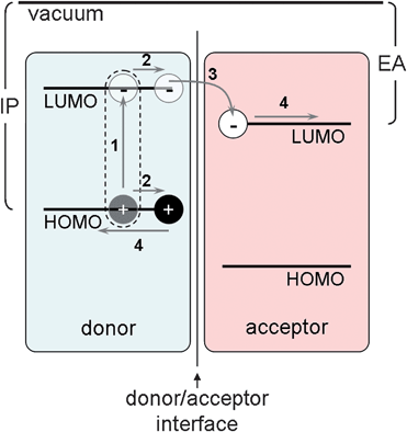 | ||
| Fig. 1 Schematic of frontier molecular orbitals (highest occupied, HOMO, and lowest unoccupied, LUMO) at a donor/acceptor interface showing steps in the photovoltaic process. Ionization potential (IP) and electron affinity (EA) are depicted for the donor and acceptor, respectively. | ||
Excitons in materials such as Si are generally bound weakly enough that ambient thermal energy is sufficient to achieve separation. Photogenerated excitons in organic semiconductors, though, are typically coulombically bound with an energy of hundreds of meV—much greater than kT.11 Moreover, the lifetime of these excitons is only on the order of ps–ns, resulting in maximum diffusion distances around 10 nm.11 Therefore, the point of each exciton generation must be within ∼10 nm of a donor/acceptor interface (Fig. 1). Once separated, the electron and hole require continuous, and preferably straight,12–14 pathways to the cathode and anode, respectively. Combining these requirements, one recognizes the need for a periodic nanostructured morphology.15–20 One could readily achieve precise control over nanoscale structuring in OPV using, for example, electron-beam or nanoimprint lithography, but these techniques have large associated costs defeating the primary purpose of switching to organic materials. One promising approach that is both capable of generating periodic, tunable nanostructures and relies upon low-cost self-assembly is the utilization of block copolymers.21
Basics of block copolymers
Block copolymers (BCPs) are macromolecules comprised of two or more homopolymer chains, or blocks, covalently bound to one another. The most common realization of this class of materials is that containing two polymer blocks—A and B—attached on one end, known as a diblock copolymer (Fig. 2a). If there is sufficient interaction between the blocks, described thermodynamically by the product of the degree of polymerization (N) and the temperature-dependent Flory–Huggins interaction parameter (χ), A–B incompatibility will drive a phase separation. The presence of a covalent bond between A and B prohibits bulk phase separation, so the polymer chains self-assemble into nanoscopic domains with a morphology that depends on the ratio of A and B block lengths, fA (Fig. 2b,2c ). The most frequently observed diblock morphologies are body-centered cubic spheres, hexagonally packed cylinders, and lamellae, though other more complex geometries have also been reported. The phase diagrams for BCPs with more than two blocks include a vastly expanded range of possible morphologies. The BCP self-assembly process can be both rationally designed and, to some degree, directed.22–24 Whereas many BCP applications require precise control over domain ordering over large length scales, such as in BCP lithography for magnetic recording media where the position of each domain must be meticulously strict due to the need for addressability, these constraints are largely relaxed for most PV applications as described in the following sections. Lateral ordering, for example, is often of minor importance compared to the presence of microphase separation and continuity of domains through the film thickness.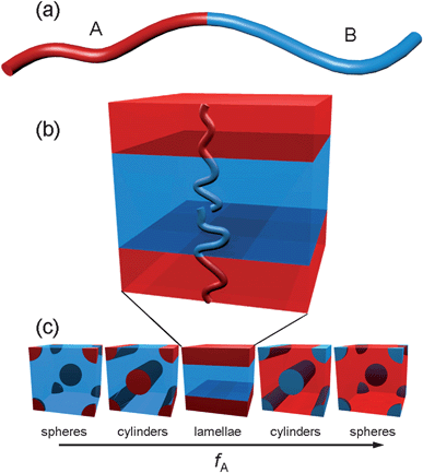 | ||
| Fig. 2 (a) Schematic representation of a diblock copolymer; (b) lamellar phase morphology depicting arrangement of polymer chains; (c) partial list of phases formed by diblock copolymers in the bulk as a function of the volume fraction of block A. Adapted from Ref. 23. | ||
Modern synthetic chemistry provides virtually limitless possibilities for BCP structure and function. The ability to design a polymer molecule with a specific length scale and geometry in mind affords an opportunity to prepare idealized nanostructures to target each of the basic steps of photovoltaic energy conversion outlined above. This review will focus on three methodologies by which BCPs currently, or have the potential to, impact research in photovoltaics: (1) BCPs as active materials, (2) BCPs as structure directors, and (3) a combination of these two approaches. In some cases these studies present the prospect of exploring structure-property relationships with unprecedented control to gain fundamental insight into self-organization and photophysical processes, whereas others may be directly applicable to technological applications. There are surely countless additional ways yet to be considered in which BCPs could impact research in solar energy.
Block copolymers as active materials
The original organic solar cells were fabricated in a bilayer architecture in which the acceptor material was deposited on top of the donor material.25 Excitonic losses severely limit the performance of this design. Typical modern organic solar cells involve a mixed donor–acceptor active layer known as a bulk heterojunction (BHJ). Such blends exhibit significant structural disorder because they rely on random phase separation of the constituents. Many domains are too large (excitonic loss), too small (charge recombination), or meandering/discontinuous (poor carrier mobility). One can imagine a BCP in which block A contains a p-type electron donor and block B contains an n-type electron acceptor. Self-assembly driven by microphase separation of such a material could, in principle, produce a highly regular nanoscale structure of idealized morphology.Theory work from Meyers et al.26 was among the first proposals to use BCPs for optoelectronics, in which they suggested using varying length blocks of conjugated polymers to manipulate the band gap energy. Actual synthesis of this class of materials was then pioneered by Jenekhe et al.27 These early studies presented evidence for efficient energy transfer from donor blocks to acceptors blocks both within a single polymer chain and between neighboring chains. In 2003, Akbayir et al. demonstrated that the self-assembly of donor–acceptor conjugated BCPs could be guided using top-down lithographic techniques.28 Combining top-down and bottom-up methodologies to manipulate self-assembly23 provides new prospects for investigating connections between nanoscale structure and function, but the need for low-cost processing will likely preclude such approaches on a commercial scale. Indeed, pure self-assembly approaches have also been shown to produce phase separated morphologies with improved nanoscale order.29 Syntheses and assembly of these so-called rod–rod BCPs (the name is derived from the rigidity of the polymer backbones) present a number of challenges,30–33 some of which can be eluded by attaching the functional moieties to the side groups rather than using the polymer backbone itself as the active material.
Another approach is to synthesize donor/acceptor rod–coil BCPs.34 Hazdiioannou et al. reported the coupling of a poly(phenylenevinylene) (PPV) block with a flexible coil block comprised of a polystyrene backbone to which C60 molecules were grafted.35–39 The (random) BHJ blend of PPV and C60 had shown promise as a PV material, but with relatively poor performance as a result of structural disorder. This work demonstrated that the rod–coil BCP approach, too, could be used to obtain efficient photoluminescence quenching and even improved photovoltaic performance by preparing self-assembled periodic nanoscale structure. A recent study has strived to enhance the photophysical interaction between the conjugated p-type polymer block and C60 by fusing the buckyballs directly into the polymer backbone.40 Another rod–coil material system recently studied by several groups is the BCP comprised of poly(3-alkylthiophene) and a polyacrylate with perylene bisimide pendant groups.41,42 These materials, which form highly crystalline domains favorable for charge carrier mobility, exhibit near total photoluminescence quenching and PV cells have been fabricated with efficiencies near 0.5%. While still an order of magnitude lower than efficiencies achieved with traditional organic BHJ cells, this result represents the current champion for a BCP PV device. Improving upon this efficiency will require additional research into molecular design and processing.
One can further extend the philosophy that the synthesis and assembly of coil polymers is often more straightforward than that of rod polymers by adopting a coil–coil BCP approach in which each block is functionalized with semiconducting side groups. Thelakkat et al. demonstrated this approach using various triphenylamine43–45 and perylene derivatives as the p- and n-type materials, respectively.46,47 Periodic nanoscale morphology and charge transfer are both successfully accomplished, and solar cells using these materials show efficiencies of about 0.3%.
When chemically bonding electron donors to acceptors as in rod–rod BCPs, one is providing an efficient pathway for excitons to separate into free charge carriers, but a direct connection can also work against PV performance because the separated carriers, whether geminate or non-geminate, can also relatively easily recombine across the same interface. Sun et al. have led the way in the design of conjugated BCPs that incorporate bridge units to investigate this issue.48–52 Specifically, alkyl- and sulfone–alkyl-substituted PPVs were utilized as the donor and acceptor moieties, respectively, while a non-conjugated structure served as a flexible bridge between them. Although the results are not compared to a donor/acceptor BCP without the bridge unit, comparisons are provided to simple blends of the donor and acceptor materials. Photoluminescence quenching and photoconductivity are both considerably increased by using the BCP methodology. Future studies specifically examining the role of the bridge unit will provide even greater insight into the photophysics of this class of materials.
It has not yet been experimentally demonstrated, but with virtually ideal nanoscale morphology, BCP active layers have the potential to readily achieve 100% IQE, that is, where every photon that is absorbed results in collected charge carriers. Overall device efficiency, however, will remain poor unless absorption can be better matched with the solar spectrum and molecular orbital energies are engineered to balance the need to achieve exciton separation while maximizing open circuit voltage. (Open circuit voltage is related to the difference between the HOMO of the donor and the LUMO of the acceptor.) Current OPV materials have band gaps that are too large for optimal sunlight absorption in single junction cells, so extensive effort is being directed at the development of low band gap polymeric materials,53 including work to incorporate such materials into BCPs.54
Recently, Krebs et al. have offered yet another pathway by which BCPs can be employed as active materials in solar cells.55,56 Their approach is highly modular, where each portion of the molecule serves a different function in the multi-step energy conversion process and is covalently linked in logical, sequential order. The core of such an integrated structure is a dyad comprised of a metalloporphyrin and a ruthenium complex, modeled after natural photosynthetic systems. Such dyads are known to exhibit high extinction coefficients and long-lived charge transfer (metal to ligand) excited states. Attached on either side of the dyad are poly(3-alkylthiophene) and PPV chains to serve as light harvesting antennae, donor/acceptor groups, and charge carrier conduits. Efficiencies of devices constructed using this paradigm are extraordinarily low, but better control over the self-assembly of these molecules will likely result in significant improvements.
Block copolymers as structure directors
Rather than using block copolymers as active materials in OPV, one can take advantage of their unusual molecular and assembly characteristics to improve the performance of organic or even hybrid organic–inorganic photovoltaic devices. Performance of polythiophene/C60 blends in PV devices is partially limited by the fact that greater than half the mass of the active layer is comprised of the fullerene, which has poor absorption properties. Replacing C60 with alternative n-type organics that maintain high electron mobility while also improving absorptivity appears to be a promising pathway toward efficiency gains. As described above, perylene diimides are proficient candidates for this role, but blends of polythiophene with perylenes produce inefficient devices due to crystallization of the perylene into domains larger than the exciton diffusion distance. Even with polythiophene/C60 blends, extended thermal annealing often leads to similarly large domain structures. BCPs can help alleviate this issue by serving as a compatibilizer that reduces interfacial tension between the component nanodomains, thereby stabilizing morphologies with domain sizes closer to the exciton diffusion scale.57,58Hybrid solar cells, including dye-sensitized cells, derive their relatively high efficiency from the nanoscale structure of the electron-accepting metal oxide material. High surface area is key, but for hybrid oxide/polymer devices, so is the balance between sufficient space among the oxide nanostructures for the polymer to form π-stacked assemblies and limiting the space to avoid exciton losses. Mesoporous titania films can be fabricated with control over their spacing and order by using BCPs as structure directors.59–61 These films are prepared by selective incorporation of titania sol–gel precursor into one block of a BCP in solution. Similar approaches can be used to obtain ordered nanostructures of a wide variety of oxide semiconductor materials,62 including non-spherical geometries such as nanorods,63 which can exhibit more effective vectorial charge transport. A related fabrication scheme involves using BCPs as structure directors to place seed catalysts into ordered arrays that subsequently provide a platform for highly oriented growth of oxide semiconductor nanorods.64
Cylindrical BCP films, when oriented perpendicular to the substrate, can provide a straightforward nanoporous template when the cylinder domains are removed by either UV or chemical degradation.65 Because the assembly occurs in parallel, this method provides a fast and low-cost route to ultra-high pore densities.66 It has been shown that semiconducting nanocrystals67 or electronically active polymer68 can be grown within these arrays. The latter scheme, achieved with electropolymerization, demonstrates an impressive level of chain alignment, which is critical for high charge carrier mobility.13 Nanoporous BCP films can also provide novel nanoelectrode arrays that may have relevance for PV applications.69
BCP lithography, where the polymer is used as a sacrificial etch mask, provides opportunities to pattern both electrodes and active layers. This technique relies on the differential etch resistance of the constituent polymer blocks to transfer the pattern of the self-assembled domains into an underlying material. The field of BCP lithography is too broad to fully cover in this short review; additional details can be found in the literature.70 Rather, here the focus is specifically on some potential applications of this technique to photovoltaics. Various BCP phases can be employed in lithographic processes, but the cylindrical phase is probably the most functional because (a) it can provide arrays of either 0-D or 1-D structures using the same starting material, assuming the cylinder orientation with respect to the substrate can be easily controlled;71,72 and (b) in the perpendicular orientation, cylinders are superior to spheres for creating high-aspect ratio features (Fig. 373) due to the lack of lower etch resistance material underneath the masking elements.
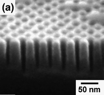 | ||
| Fig. 3 Scanning electron micrograph of high-aspect-ratio silicon structures fabricated using block copolymer lithography. Reproduced with permission from Ref. 73. | ||
If there were a way to efficiently pull charge carriers out from deep within an active layer in a solar cell, many performance problems associated with charge carrier migration and recombination could be addressed. A reasonable geometry to accomplish this task would be to fabricate an electrode (or, better, both electrodes) with nanoscale pillars that would be inserted into the active layer rather than relying on a planar architecture. This approach would drastically reduce the distance a charge carrier would have to travel through the lower mobility semiconducting material and thereby increase the device photocurrent. BCPs are nearly ideal masks for creating interfaces of this nature.
Alternatively, one can use BCP lithography to directly pattern the active layer while using traditional planar electrodes. This methodology can be applied to either organic or inorganic materials. Several groups have shown that electronically active polymers can be patterned using BCP masks without adverse effect on their physical properties.74,75 Such a scheme could be used to create a nanoporous film of, say, p-type polymer that could then be infiltrated with complementary n-type materials such as C60 to create a highly ordered bulk heterojunction in contrast to the random phase separated structure achieved with blends. Inorganic materials can also benefit from such nanostructuring because inexpensive materials typically have low minority carrier diffusion lengths resulting from impurities or defects. A nanorod array comprised of p-type material conformally coated with a layer of n-type material would again take advantage of the concept of separating the dimensions of light absorption and carrier extraction.76 Indeed, materials such as silicon have been successfully patterned into nanorod arrays with aspect ratios as large as 10:1 using BCP lithography.77 A conformal deposition technique such as atomic layer deposition78 could be used to coat an appropriately doped silicon array with a complementary semiconductor material to provide for radial charge collection.
Block copolymers as both active materials and structure directors
In the previous two sections, opportunities for application of BCPs either directly as active materials or indirectly as structure directors of PV device components were discussed. A third potential area, which is to date the least explored, is to merge these notions and utilize BCPs where one or more of the blocks is conjugated to organize additional active material in a PV application. Hybrid solar cells comprised of mixtures of conjugated polymers and semiconductor nanorods are of interest due to the enhanced charge separation and electron mobility imparted by the inorganic components.79,80 Rather than replace the organic acceptor with nanocrystals, there are also advantages to simply adding nanocrystals to traditional organic donor/acceptor blends. EQEs exceeding 100% have been reported with this approach.81 A constant challenge with hybrid mixtures such as these is spontaneous nanoparticle aggregation, particularly upon annealing. Macroscopic assemblies of nanoparticles hinder performance. In fact, most hybrid active layers contain excess quantities of nanoparticles to compensate for the aggregate material wasted within such assemblies. In order to overcome these problems, it is necessary to provide structure direction. BCPs have been shown to excel at selective placement of nanocrystals,82–85 and even continuous inorganic materials,86,87 into periodic morphologies.Because conjugated polymers often have band gaps that are larger than ideal for harvesting sunlight, one pathway to increase device efficiency is to use semiconductor nanocrystals as the chromophores and have the polymer block(s) fill the role of charge carrier transport. Gratt and Cohen designed a triblock copolymer to achieve the three-fold goals of hole transport, nanoparticle binding, and electron transport.88 All three moieties were based on norbornene, with long chain carbazole and dinitrobenzene derivatives as the hole- and electron-transport materials, respectively, whereas the short central block was designed to bind passivated CdSe quantum dots. Interactions between the polymer and nanoparticles effectively inhibit aggregation of the latter. By manipulating the processing conditions to prepare either disordered or cylindrical microphase-separated morphologies in PV devices, they were able to show that BCP ordering improved the charge collection efficiency. A simpler design aimed at merging the chromophore and electron transport responsibilities into one material has been reported by Thelakkat et al.89 In this case, a diblock copolymer is used in which one block contains tetraphenylbenzidine pendant groups with hole-transport capability and the other block, poly(4-vinylpyridine) (P4VP), will selectively take up semiconductor nanoparticles and prevent their agglomeration. The block volume fractions were designed to form lamellar structures, which are not qualitatively affected by the presence of the nanocrystals. In this case, CdSe:Te particles were chosen as the light harvesting and electron transport material, though many other compositions would likely behave similarly. More studies will be required to ascertain, and ultimately optimize, the degree of electronic communication between the particles sequestered in the P4VP domains—as well as the electronic role, if any, of that polymeric matrix, but this methodology appears promising as a facile route to the fabrication of periodic nanostructured hybrid active layers.
Polymer blocks that display selective nanoparticle binding do a good job of preventing unwanted macroscopic particle aggregation, but they may also interfere with optoelectronic processes critical to photovoltaic energy conversion. An alternative strategy to incorporation of nanocrystals, or indeed virtually any nanomaterial, that circumvents this concern is based on ideas related to the BCP nanoporous templates described in the previous section. The difference here is that the block(s) comprising the matrix surrounding the nanoscopic pores is/are an active participant in the light harvesting and/or charge carrier transport. Such an approach offers tremendous flexibility in that the synthetic target would typically be a rod–coil polymer, permitting nearly any polymer to be chosen for the conjugated block because of the solubility and non-crystallizable nature of the coil block. Furthermore, the pores could be infiltrated with any of a wide variety of complementary optoelectronic nanomaterials.
Poly(methylmethacrylate) is a popular block that can be easily degraded using a combination of UV light and an acetic acid rinse, but UV light will often trigger photochemical changes in the conjugated block, which may be detrimental to performance. A less damaging option is to use polylactide (PLA), which can be degraded using a gentler alkaline solution treatment. Hillmyer et al. recently reported the first synthesis of a rod–coil BCP using this concept.90 They prepared a poly(3-alkylthiophene)–PLA BCP and demonstrated that films of this material deposited on conductive substrates would microphase separate into lamellae. Moreover, the rod blocks formed crystalline domains, which are expected to have reasonably high hole mobility. Treatment of the BCP films produced nanoporous layers, as observed with atomic force microscopy.
The application of this BCP has recently been further explored for photovoltaics. Using a similar BCP, spontaneous formation of lamellar domains has been observed, that is, immediately after spin casting without any need for solvent or thermal annealing.91 OPV devices generally require a layer between the active material and the transparent conductive substrate whose purpose is to transmit holes and block electrons; a mixture of ionic polymers (PEDOT:PSS) is a common choice for this layer. It has been shown that microphase separation occurs readily on this surface with similar quality to that achieved by direct deposition on the transparent conductor (Fig. 4). Spectroscopic measurements demonstrate that after complete degradation of the PLA block to form a nanoporous film the thiophene polymer remains chemically intact. Coupling to an electron acceptor is achieved by exposure to an aqueous solution of C60. Photoluminescence data confirm that charge transfer does occur from the p-type polymer to this fullerene species,92 indicating promise for this fabrication method for highly ordered, low-cost organic or hybrid PV active layers. There are, however, continuing challenges associated with realizing this potential. Namely, (a) lateral domain collapse occurs after removal of the PLA domains, which increases the length scale of the structural periodicity beyond the exciton diffusion distance, and (b) traditional hole-transport layer materials are not compatible with the processing described above because they will delaminate upon exposure to an aqueous environment; a suitable material impervious to both organic and aqueous solvents needs to be identified.
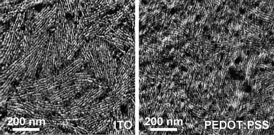 | ||
| Fig. 4 Atomic force micrograph phase images of rod–coil block copolymer films prepared on indium tin oxide (ITO) and poly(3,4-ethylenedioxythiophene):poly(styrenesulfonate) (PEDOT:PSS)/ITO substrates showing lamellar morphology. | ||
Conclusions
In order to achieve the full potential of photovoltaic conversion for supplying energy needs worldwide, lower cost materials and processes are required. Control over nanoscale morphology is critical to obtain acceptable efficiencies using suitable materials, and BCPs provide a versatile platform for realizing this control. This is a nascent research area, and much work remains to be done in topics ranging from synthesis of rationally designed optoelectronic BCPs to investigations of self-organization of BCP and BCP/nanomaterial hybrid films to photophysical characterization of these fascinating systems. Efficiencies of solar cells fabricated using BCPs have yet to exceed—or even match—those obtained from traditional bulk heterojunction systems, but as additional insights are derived from ongoing and future studies into BCP PV, significant advances are expected.This minireview is designed to provide the reader with the motivation driving this field, some of the associated challenges, and a summary of a few recent endeavors. It is anticipated that possibilities not discussed here will occur to readers both for pushing forward those directions outlined above and for new directions in nanostructure engineering for photovoltaics with BCPs.
Acknowledgements
Use of the Center for Nanoscale Materials was supported by the U.S. Department of Energy, Office of Science, Office of Basic Energy Sciences, under Contract No. DE-AC02-06CH11357.References
- N. S. Lewis, Science, 2007, 315, 798–801 CrossRef CAS.
- W. Shockley and H. J. Queisser, J. Appl. Phys., 1961, 32, 510–519 CAS.
- N. S. Lewis and G. Crabtree, Basic Research Needs for Solar Energy Utilization, Department of Energy, 2005 Search PubMed.
- L. L. Kazmerski, J. Electron Spectrosc. Relat. Phenom., 2006, 150, 105–135 CrossRef CAS.
- W. Brutting, ed., Physics of Organic Semiconductors, Wiley-VCH, Weinheim, 2005 Search PubMed.
- C. Brabec, V. Dyakonov, J. Parisi and N. S. Sariciftci, eds., Organic Photovoltaics: Concepts and Realization, Springer-Verlag, New York, 2003 Search PubMed.
- S.-S. Sun and N. S. Sariciftci, eds., Organic Photovoltaics: Mechanisms, Materials, and Devices, Taylor & Francis, New York, 2005 Search PubMed.
- J. Y. Kim, K. Lee, N. E. Coates, D. Moses, T.-Q. Nguyen, M. Dante and A. J. Heeger, Science, 2007, 317, 222–225 CrossRef CAS.
- Plextronics' Organic Solar Cell Technology Breaks World Record:National Renewable Energy Laboratory Certifies Cell Efficiency, http://www.plextronics.com/press_detail.aspx%3FPressReleaseID%3D7.
- There are additional obstacles associated with environmental stability of OPV materials that are outside the scope of this article.
- M. Knupfer, Appl. Phys. A: Mater. Sci. Process., 2003, 77, 623–626 CrossRef CAS.
- V. Coropceanu, J. Cornil, D. A. da Silva Filho, Y. Olivier, R. Silbey and J.-L. Brédas, Chem. Rev., 2007, 107, 926–952 CrossRef CAS.
- S. B. Darling, J. Phys. Chem. B, 2008, 112, 8891–8895 CrossRef CAS.
- S. B. Darling and M. Sternberg, J. Phys. Chem. B, 2009, 113, 6215–6218 CrossRef CAS.
- C. R. McNeill, B. Watts, L. Thomsen, H. Ade, N. C. Greenham and P. C. Dastoor, Macromolecules, 2007, 40, 3263–3270 CrossRef CAS.
- E. H. A. Beckers, Z. Chen, S. C. J. Meskers, P. Jonkheijm, A. P. H. J. Schenning, X.-Q. Li, P. Osswald, F. Wurthner and R. A. J. Janssen, J. Phys. Chem. B, 2006, 110, 16967–16978 CrossRef CAS.
- X. Yang and J. Loos, Macromolecules, 2007, 40, 1353–1362 CrossRef CAS.
- S. Tepavcevic, S. B. Darling, N. M. Dimitrijevic, T. Rajh and S. J. Sibener, Small, 2009, 5, 1776 CrossRef CAS.
- K. M. Coakley and M. D. McGehee, Chem. Mater., 2004, 16, 4533–4542 CrossRef CAS.
- M. Grätzel, Philos. Trans. R. Soc. London, Ser. A, 2007, 365, 993–1005 CrossRef CAS.
- F. S. Bates and G. H. Fredrickson, Phys. Today, 1999, 52, 32–38 CrossRef CAS.
- R. A. Segalman, Mater. Sci. Eng., R, 2005, 48, 191–226.
- S. B. Darling, Prog. Polym. Sci., 2007, 32, 1152–1204 CrossRef CAS.
- J. Y. Cheng, C. A. Ross, H. I. Smith and E. L. Thomas, Adv. Mater., 2006, 18, 2505–2521 CrossRef CAS.
- C. W. Tang, Appl. Phys. Lett., 1986, 48, 183–185 CrossRef CAS.
- F. Meyers, A. J. Heeger and J. L. Brédas, J. Chem. Phys., 1992, 97, 2750–2758 CrossRef CAS.
- X. L. Chen and S. A. Jenekhe, Macromolecules, 1996, 29, 6189–6192 CrossRef CAS.
- C. Akbayir, F. Bulut, T. Farrell, A. Goldschmidt, R. Gunter, A. P. Kam, P. Miclea, U. Scherf, J. Seekamp, V. G. Solovyev and C. M. Sotomayor-Torres, Rev. Adv. Mater. Sci., 2003, 5, 205–210 CAS.
- G. Tu, H. Li, M. Forster, R. Heiderhoff, L. G. Balk and U. Scherf, Macromolecules, 2006, 39, 4327–4331 CrossRef CAS.
- U. Scherf, A. Gutacker and N. Koenen, Acc. Chem. Res., 2008, 41, 1086–1097 CrossRef CAS.
- P.-T. Wu, G. Ren, C. Li, R. Mezzenga and S. A. Jenekhe, Macromolecules, 2009, 42, 2317–2320 CrossRef CAS.
- K. Ohshimizu and M. Ueda, Macromolecules, 2008, 41, 5289–5294 CrossRef CAS.
- Q. Peng, K. Park, T. Lin, M. Durstock and L. Dai, J. Phys. Chem. B, 2008, 112, 2801–2808 CrossRef CAS.
- Y. Liang, H. Wang, S. Yuan, Y. Lee, L. Gan and L. Yu, J. Mater. Chem., 2007, 17, 2183–2194 RSC.
- U. Stalmach, B. de Boer, C. Videlot, P. F. van Hutten and G. Hadziioannou, J. Am. Chem. Soc., 2000, 122, 5464–5472 CrossRef CAS.
- B. de Boer, U. Stalmach, P. F. van Hutten, C. Melzer, V. V. Krasnikov and G. Hadziioannou, Polymer, 2001, 42, 9097–9109 CrossRef CAS.
- M. H. van der Veen, B. de Boer, U. Stalmach, K. I. van de Wetering and G. Hadziioannou, Macromolecules, 2004, 37, 3673–3684 CrossRef CAS.
- S. Barrau, T. Heiser, F. Richard, C. Brochon, C. Ngov, K. van de Wetering, G. Hadziioannou, D. V. Anokhin and D. A. Ivanov, Macromolecules, 2008, 41, 2701–2710 CrossRef CAS.
- C. Brochon, N. Sary, R. Mazzenga, C. Ngov, F. Richard, M. May and G. Hadziioannou, J. Appl. Polym. Sci., 2008, 110, 3664–3670 CrossRef CAS.
- R. C. Hiorns, P. Iratcabal, D. Begue, A. Khoukh, R. de Bettignies, J. Leroy, M. Firon, C. Sentein, H. Martinez, H. Preud'homme and C. Dagron-Lartigau, J. Polym. Sci., Part A: Polym. Chem., 2009, 47, 2304–2317 CrossRef CAS.
- M. Sommer, A. S. Lang and M. Thelakkat, Angew. Chem., Int. Ed., 2008, 47, 7901–7904 CrossRef CAS.
- Q. Zhang, A. Cirpan, T. P. Russell and T. Emrick, Macromolecules, 2009, 42, 1079–1082 CrossRef CAS.
- M. Behl, E. Hattemer, M. Brehmer and R. Zentel, Macromol. Chem. Phys., 2002, 203, 503–510 CrossRef CAS.
- K. Peter and M. Thelakkat, Macromolecules, 2003, 36, 1779–1785 CrossRef CAS.
- G. N. Tew, M. U. Pralle and S. I. Stupp, Angew. Chem., 2000, 112, 527–531 CrossRef.
- M. Sommer, S. M. Lindner and M. Thelakkat, Adv. Funct. Mater., 2007, 17, 1493–1500 CrossRef CAS.
- S. M. Lindner and M. Thelakkat, Macromolecules, 2004, 37, 8832–8835 CrossRef CAS.
- S. Sun, Z. Fan, Y. Wang, J. Haliburton, C. Taft, S. Maaref, K. Seo and C. E. Bonner, Synth. Met., 2003, 137, 883–884 CrossRef CAS.
- S.-S. Sun, Sol. Energy Mater. Sol. Cells, 2003, 79, 257–264 CrossRef CAS.
- S.-S. Sun, C. Zhang, A. Ledbetter, S. Choi, K. Seo, C. E. Bonner, M. Drees and N. S. Sariciftci, Appl. Phys. Lett., 2007, 90, 043117 CrossRef.
- C. Zhang, S. Choi, J. Haliburton, T. Cleveland, R. Li, S.-S. Sun, A. Ledbetter and C. E. Bonner, Macromolecules, 2006, 39, 4317–4326 CrossRef CAS.
- S.-S. Sun, Z. Fan, Y. Wang and J. Haliburton, J. Mater. Sci., 2005, 40, 1429–1443 CrossRef CAS.
- E. Bundgaard and F. C. Krebs, Sol. Energy Mater. Sol. Cells, 2007, 91, 954–985 CrossRef CAS.
- K. Van de Wetering, C. Brochon, C. Ngov and G. Hadziioannou, Macromolecules, 2006, 39, 4289–4297 CrossRef.
- O. Hagemann, M. Jorgensen and F. C. Krebs, J. Org. Chem., 2006, 71, 5546–5559 CrossRef CAS.
- F. C. Krebs, O. Hagemann and M. Jorgensen, Sol. Energy Mater. Sol. Cells, 2004, 83, 211–228 CrossRef CAS.
- K. Sivula, Z. T. Ball, N. Watanabe and J. M. J. Frechet, Adv. Mater., 2006, 18, 206–210 CrossRef CAS.
- S. Rajaram, P. B. Armstrong, B. J. Kim and J. M. J. Frechet, Chem. Mater., 2009, 21, 1775–1777 CrossRef CAS.
- K. M. Coakley and M. D. McGehee, Appl. Phys. Lett., 2003, 83, 3380–3382 CrossRef CAS.
- Z. Sun, Y. Cheng, M. Lechmann, J. Li, J. Li, J. Wu, A. Grimsdale, K. Mullen, H.-J. Butt and J. S. Gutmann, Phys. Chem. Chem. Phys., 2009, 11, 1604–1609 RSC.
- J. Perlich, M. Memesa, A. Diethert, E. Metwalli, W. Wang, S. V. Roth, A. Timmann, J. S. Gutmann and P. Muller-Buschbaum, ChemPhysChem, 2009, 10, 799–805 CrossRef CAS.
- J. P. Spatz, S. Mössmer, C. Hartmann, M. Möller, T. Herzog, M. Krieger, H.-G. Boyen, P. Ziemann and B. Kabius, Langmuir, 2000, 16, 407–415 CrossRef CAS.
- X. Jia, W. He, X. Zhang, H. Zhao, Z. Li and Y. Feng, Nanotechnology, 2007, 18, 075602 CrossRef.
- M. Haupt, A. Ladenburger, R. Sauer, K. Thonke, R. Glass, W. Roos, J. P. Spatz, H. Rauscher, S. Riethmüller and M. Möller, J. Appl. Phys., 2003, 93, 6252–6257 CrossRef CAS.
- D. A. Olson, L. Chen and M. A. Hillmyer, Chem. Mater., 2008, 20, 869–890 CrossRef CAS.
- T. Thurn-Albrecht, R. Steiner, J. DeRouchey, C. M. Stafford, E. Huang, M. Bal, M. Tuominen, C. J. Hawker and T. P. Russell, Adv. Mater., 2000, 12, 787–791 CrossRef CAS.
- K.-H. Lo, W.-H. Tseng and R.-M. Ho, Macromolecules, 2007, 40, 2621–2624 CrossRef CAS.
- J. I. Lee, S. H. Cho, S.-M. Park, J. K. Kim, J. K. Kim, J.-W. Yu, Y. C. Kim and T. P. Russell, Nano Lett., 2008, 8, 2315–2320 CrossRef CAS.
- E. Jeoung, T. H. Galow, J. Schotter, M. Bal, A. Ursache, M. T. Tuominen, C. M. Stafford, T. P. Russell and V. M. Rotello, Langmuir, 2001, 17, 6396–6398 CrossRef CAS.
- C. J. Hawker and T. P. Russell, MRS Bull., 2005, 30, 952–966 CAS.
- D. A. Rider, K. A. Cavicchi, L. Vanderark, T. P. Russell and I. Manners, Macromolecules, 2007, 40, 3790–3796 CrossRef CAS.
- M. Ramanathan, E. Nettleton and S. B. Darling, Thin Solid Films, 2009, 517, 4474–4478 CrossRef CAS.
- C. T. Black, Custom Integrated Circuits Conference, San Jose, CA, 2005 Search PubMed.
- Y. S. Jung, W. Jung, H. L. Tuller and C. A. Ross, Nano Lett., 2008, 8, 3776–3780 CrossRef CAS.
- X. Li, S. Tian, Y. Ping, D. H. Kim and W. Knoll, Langmuir, 2005, 21, 9393–9397 CrossRef CAS.
- B. M. Kayes, C. E. Richardson, N. S. Lewis and H. A. Atwater, Photovoltaic Specialists Conference, 2005 Search PubMed.
- V. Gowrishankar, N. Miller, M. D. McGehee, M. J. Misner, D. Y. Ryu, T. P. Russell, E. Drockenmuller and C. J. Hawker, Thin Solid Films, 2006, 513, 289–294 CrossRef CAS.
- A. B. F. Martinson, J. W. Elam, J. Liu, J. T. Hupp and M. J. Pellin, Nano Lett., 2008, 8, 2862–2866 CrossRef CAS.
- W. U. Huynh, J. J. Dittmer and A. P. Alivisatos, Science, 2002, 295, 2425–2427 CrossRef CAS.
- M. Brinkmann, D. Aldakov and F. Chandezon, Adv. Mater., 2007, 19, 3819 CrossRef CAS.
- H.-Y. Chen, M. K. F. Lo, G. Yang, H. G. Monbouquette and Y. Yang, Nat. Nanotechnol., 2008, 3, 543–547 Search PubMed.
- D. E. Fogg, L. H. Radzilowski, B. O. Dabbousi, R. R. Schrock, E. L. Thomas and M. G. Bawendi, Macromolecules, 1997, 30, 8433–8439 CrossRef CAS.
- M. R. Bockstaller, Y. Lapetnikov, S. Margel and E. L. Thomas, J. Am. Chem. Soc., 2003, 125, 5276–5277 CrossRef CAS.
- S. B. Darling, N. A. Yufa, A. L. Cisse, S. D. Bader and S. J. Sibener, Adv. Mater., 2005, 17, 2446–2450 CrossRef CAS.
- S. B. Darling, Surf. Sci., 2007, 601, 2555–2561 CrossRef CAS.
- W. A. Lopes and H. M. Jaeger, Nature, 2001, 414, 735–738 CrossRef CAS.
- S. B. Darling and A. Hoffmann, J. Vac. Sci. Technol., A, 2007, 25, 1048–1051 CrossRef CAS.
- J. A. Gratt and R. E. Cohen, J. Appl. Polym. Sci., 2004, 91, 3362–3368 CrossRef CAS.
- S. Maria, A. S. Susha, M. Sommer, D. V. Talapin, A. L. Rogach and M. Thelakkat, Macromolecules, 2008, 41, 6081–6088 CrossRef CAS.
- B. W. Boudouris, C. D. Frisbie and M. A. Hillmyer, Macromolecules, 2008, 41, 67–75 CrossRef CAS.
- I. Botiz and S. B. Darling, Rational Design of Nanostructured Hybrid Materials for Photovoltaics, in Active Polymers, ed. A. Lendlein, V. Prasad Shastri and K. Gall, (Mat. Res. Soc. Symp. Proc.), Warrendale, PA, 2009, vol. 1190, Search PubMed1190-NN03-20.
- I. Botiz and S. B. Darling, Macromolecules, 2009 DOI:10.1021/ma901420h.
| This journal is © The Royal Society of Chemistry 2009 |