Organic photovoltaics
Bernard
Kippelen
*a and
Jean-Luc
Brédas
b
aSchool of Electrical and Computer Engineering, Center for Organic Photonics and Electronics, Georgia Institute of Technology, Atlanta, Georgia 30332, USA. E-mail: kippelen@gatech.edu
bSchool of Chemistry and Biochemistry, Center for Organic Photonics and Electronics, Georgia Institute of Technology, Atlanta, Georgia 30332, USA
First published on 7th January 2009
Abstract
Organic photovoltaics, the technology to convert sun light into electricity by employing thin films of organic semiconductors, has been the subject of active research over the past 20 years and has received increased interest in recent years by the industrial sector. This technology has the potential to spawn a new generation of low-cost, solar-powered products with thin and flexible form factors. Here, we introduce the energy and environmental science community to the basic concepts of organic photovoltaics and discuss some recent science and engineering results and future challenges.
 Bernard Kippelen Bernard Kippelen | Bernard Kippelen received his PhD in solid-state physics in 1990 from the University Louis Pasteur, Strasbourg, France. He was Chargé de Recherches at the CNRS. In 1994 he joined the Optical Sciences Center at The University of Arizona where he became an Assistant Professor in 1998 and an Associate Professor in 2001. Since 2003, he has been Professor of Electrical and Computer Engineering at the Georgia Institute of Technology, Atlanta, USA. He is a Fellow of the Optical Society of America, a Fellow of SPIE, and a Senior Member of IEEE. |
 Jean-Luc Brédas Jean-Luc Brédas | Jean-Luc Brédas received his PhD in Chemistry from the University of Namur, Belgium, in 1979. In 1988, he was appointed Professor at the University of Mons-Hainaut, Belgium. He joined the University of Arizona in 1999 before moving in 2003 to the Georgia Institute of Technology where he is a Professor of Chemistry and Biochemistry. He is the recipient of the 1997 Francqui Prize, the 2000 Quinquennial Prize of the Belgian National Science Foundation, the 2001 Italgas Prize (shared with Richard Friend), and a member of the team laureate of the 2003 Descartes Prize of the European Union. |
Broader contextOrganic photovoltaics, the technology to convert sun light into electricity by employing thin films of organic semiconductors, has been the subject of active research over the past 20 years and has received increased interest in recent years by the industrial sector. This technology has the potential to spawn a new generation of low-cost, solar-powered products with thin and flexible form factors. This review introduces the energy and environmental science community to the basic concepts of organic photovoltaics and discusses some recent science and engineering results and future challenges. |
The photovoltaic effect—the conversion of light into electrical power—can be traced back to Becquerel's 1839 pioneering studies in liquid electrolytes1 and has since been studied in a wide range of materials. In the modern era, the tipping point that transformed photovoltaics into a technology to convert sun light into electricity was the 1954 report by Chapin et al.2 of a silicon-based single p–n junction device with a solar power conversion efficiency of 6%. Recognized initially as a sustainable power source for geostationary communications satellites, photovoltaic cells have now gained in efficiency and found many applications in the consumer market.3–5 More importantly, in recent years, they are emerging as a clean and sustainable source of energy and are expected to play a major role in meeting the global energy challenge.6
Solar technologies are currently dominated by wafer-size single-junction solar cells based on crystalline silicon that are assembled into large area modules. However, other semiconductor materials and devices are under active investigation in order to further reduce the cost of produced electricity by: increasing the power conversion efficiency, reducing the amount of absorbing material needed, and lowering the assembly cost of modules. Thin-film photovoltaic technologies,7 referred to as second-generation photovoltaics, are based on inorganic semiconductor materials that are more absorbing than crystalline silicon and can be processed directly onto large area substrates. Such semiconductors include amorphous silicon, II–VI semiconductors such as CdS or CdTe, and chalcogenides such as CuInSe2 (CIS) or CuInGaSe2 (CIGS).8 Despite the laboratory demonstration of cells with high efficiencies (19% for CIGS9 and 16% for CdTe10), the controlled manufacturing of second-generation cells remains a challenge and their commercial use is growing but not as widespread yet.
Simultaneously, over the past two decades, the science and engineering of organic semiconducting materials have advanced very rapidly, leading to the demonstration and optimization of a range of organics-based solid-state devices, including organic light-emitting diodes (OLEDs),11 field-effect transistors,12,13 photodiodes,14 and photovoltaic cells. Seeded in the 1960s by fundamental studies on the optical and electronic properties of model organic molecules such as acenes15—molecules based on up to five fused benzene rings—this area of research gained significant momentum in the late 1970s and in the 1980s when high-purity small organic molecules with tailored structure and properties were synthesized and processed at room temperature into thin films using physical vapor deposition techniques. Building on such advances, Tang16 developed single heterojunction organic photovoltaic cells and reported in 1986 a power conversion efficiency of about 1%. This result represented a major milestone and a significant improvement in efficiency over the first report of a device with similar geometry by Kearns and Calvin17 in 1958. The advent in the 1990's of high-purity conjugated polymers allowed the fabrication of organic photovoltaic cells with materials simply processed from solution.18,19
The low-temperature processing of either organic small molecules from the vapor phase or polymers from solution confers organic semiconductors with a critical advantage over their inorganic counterparts, as the high-temperature processing requirements of the latter limit the range of substrates on which they can be deposited. Particularly attractive for organic semiconductors are flexible plastic substrates that can lead to applications and consumer products with lower cost, highly flexible form factors, and light weight. Furthermore, low-temperature processing cuts on energy use during manufacturing, further reducing the energy payback time which is defined as the operating life of a power-generating device needed to produce the amount of energy invested during manufacturing, installation and maintenance. These attributes, combined with the ability to tune the physical properties of organic (macro)molecules by fine tuning their chemical structure, constitute the main drivers boosting research and industrial interest in organic photovoltaics.
The organics-based approaches and those that do not rely on conventional single p–n junctions are often referred to as third-generation technologies. They include: (i) the dye-sensitized solar cells pioneered by Grätzel,20,21 which are electrochemical cells that require an electrolyte; (ii) multijunction cells fabricated from group IV and III–V semiconductors;22 (iii) hybrid approaches in which inorganic quantum dots23–25 are doped into a semiconducting polymer matrix or by combining nanostructured inorganic semiconductors such as TiO2 with organic materials;26–30 (iv) and all-organic solid-state approaches. In this article we will focus mainly on the latter.
While the physics of conventional p–n junctions is reasonably well understood and solar cell properties can be derived from materials parameters and the nature of the electrical contacts with electrodes, the understanding of the underlying science of organic solar cells is far less advanced and remains an intense subject of research. For instance, a key difference in the physics of organic semiconductors compared to their inorganic counterparts is the nature of the optically excited states. The absorption of a photon in organic materials leads to the formation of an exciton, i.e., a bound electron–hole pair. The exciton binding energy is typically large, on the order of or larger than 500 meV (such binding energies represent twenty times or more the thermal energy at room temperature, kT(300 K) = 26 meV,31,32 to be compared with a few meV in the case of inorganic semiconductors. Consequently, optical absorption in organic materials does not lead directly to free electron and hole carriers that could readily generate an electrical current. Instead, to generate a current, the excitons must first dissociate. The excitonic character of their optical properties is a signature feature of organic semiconductors, which has impacted the design and geometry of organic photovoltaic devices for the past decades.
Our objective in this review is to introduce organic photovoltaics to the general energy and environmental science community. We discuss the science and engineering of solid-state organic photovoltaic materials and devices with an emphasis on the physical processes involved in the operation of these devices and the comparison with traditional inorganic p–n devices. Thus, we do not intend to provide a comprehensive survey of the wide range of materials and device geometries that have been developed; to get more familiar with the latter topics, we refer the reader to excellent recent reviews.14,33–37
Materials and device structures
Organic molecular and polymeric semiconductors can form films with complex morphologies and varying degrees of order and packing modes through the interplay of a variety of non-covalent interactions. Their molecular structure consistently presents a backbone along which the carbon (or nitrogen, oxygen, sulfur) atoms are sp2-hybridized and thus possess a π-atomic orbital. The conjugation (overlap) of these π orbitals along the backbone results in the formation of delocalized π molecular orbitals, which define the frontier (HOMO and LUMO) electronic levels and determine the optical and electrical properties of the (macro)molecules. The overlap of the frontier π molecular orbitals between adjacent molecules or polymer chains characterizes the strength of the intermolecular electronic couplings (also called transfer integrals or tunneling matrix elements), which represent the key parameter governing charge carrier mobilities. In crystalline inorganic semiconductors, the three-dimensional character and rigidity of the lattice ensure wide valence and conduction bands and large charge carrier mobilities (typically on the order of several 102 to 103 cm2V−1 s−1). In contrast, in organic semiconductors, the weakness of the electronic couplings (due to their intermolecular character), the large electron–vibration couplings (leading to pronounced geometry relaxations), and the disorder effects all conspire to produce more modest carrier mobilities due to charge-carrier localization and formation of polarons; transport then relies on polarons hopping from molecule to molecule (here and in the remainder of the text, “molecule” should also be taken as meaning “polymer chain segment” where appropriate).38 As a result, the charge carrier mobilities strongly depend on the morphology and can vary over several orders of magnitude when going from highly disordered amorphous films (typically, 10−6 to 10−3 cm2V−1 s−1) to highly ordered crystalline materials (>1 cm2V−1 s−1).38 To describe the operation of organic solar cells, energy diagrams can be drawn in which the valence and conduction band energies are replaced by the HOMO and LUMO (polaron level) energies, respectively.39The general structure of an organic photovoltaic device similar to that reported by Tang16 in 1986 is shown in Fig. 1. It consists of a transparent electrode, typically a conducting oxide such as indium-tin oxide (ITO), two organic light-absorbing layers, and a second electrode. The two organic layers are made of different organic semiconductors, one with an electron-donor character and the other with an electron-acceptor character. Electron-donor molecules (D) exhibit a low ionization potential (and thus a high-lying HOMO energy), while electron-acceptor molecules (A) possess a high electron affinity (and thus a low-lying LUMO energy) (see Fig. 1). The D and A layers must provide for efficient hole and electron transport, respectively.
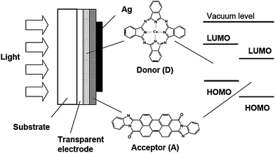 | ||
| Fig. 1 Cross-section of a bilayer organic solar cell. Chemical structure of examples of donor and acceptor molecules used in the seminal work of Tang. Donor: copper-phthalocyanine; acceptor: perylene tetracarboxylic derivative. | ||
To compare the operation of an organic solar cell with conventional cells and to highlight their fundamental differences, it is useful to review the operation of inorganic solar cells based on p–n junctions. When an abrupt p–n junction is formed from doped inorganic semiconductors, the carrier distributions and concentrations in the materials under equilibrium conditions can be modeled and derived from the semiconductors parameters and the properties of their interfaces with the electrodes.40,41 The condition of invariance of the equilibrium Fermi level leads to the conventional band energy diagram used to describe a p–n junction in which the energies of the valence band and conduction band are position dependent near the junction (see Fig. 2a). The charge redistribution that takes place near the junction (in the depletion region) leads to a built-in potential and to an electric field that is confined to the vicinity of the junction. Assuming constant doping on each side of the junction, the electric field outside the depletion region vanishes. Illumination of the materials leads to photogenerated electron/hole pairs, for which excitonic effects can be ignored at room temperature. The excess of photogenerated electrons in the n-doped semiconductor and holes in the p-doped side of the junction are negligible compared to the densities of majority carriers on both sides at thermal equilibrium. In contrast, electron and hole densities created in the p-doped and n-doped semiconductors, respectively, are significant relative to the densities of minority carriers at equilibrium in the dark. Carrier transport generally occurs inside the semiconductors mainly through a combination of drift and diffusion. At the junction, the minority carriers are swept away through a drift process due to the junction potential. Away from the junction, the transport of the minority carriers is mainly governed by diffusion. In such conditions, the photocurrent density of a conventional inorganic solar cell can be derived from the minority carrier diffusion equations obtained by combining the continuity and current equations. Solutions are found by considering the boundary conditions in which the photogenerated minority carriers at the junction are zero and where the interfaces of the semiconductors with the front and back electrodes are characterized by surface recombination velocities.40,41
![Comparison of the energy level diagrams for inorganic and organic solar cells. (a) Energy levels in an inorganic p–n junction under illumination. εFe and εFh denote the quasi-Fermi levels in the n-type and p-type semiconductors. The difference between the quasi-Fermi level energies determines the maximum open-circuit voltage (VOC) under illumination. Absorption of photons with an average photon energy larger than the band gap on either side of the junction in the n-type and p-type semiconductors (step 1) is followed by thermalization of the holes and electrons near the top of the valence and conduction bands, respectively (step 2). Minority carriers (electrons in the p-type semiconductor; holes in the n-type semiconductor) diffuse to the junction where they are swept away and accumulate on the other side of the junction where they become majority carriers (step 3). For the sake of simplicity, these three steps have been drawn for electrons, but the same applies to holes. (b) Energy level diagram of an organic heterojunction under illumination. IP(D) and EA(A) denote the ionization potential (HOMO level energy) of the donor molecular layer and the electron affinity (LUMO level energy) of the acceptor molecular layer, respectively. Absorption of photons with an average photon energy larger than the optical band gap on either side of the heterojunction (step 1) is followed by thermalization and the formation of excitons (step 2). Excitons diffuse to the heterojunction (step 3) where they dissociate and transfer an electron [hole] into the acceptor [donor] layer (step 4). The difference between IP(D) and EA(A) determines the maximum open circuit voltage (VOC) under illumination. The Δ arrows denote the energy offsets between the ionization potential values (HOMO energies) and electron affinities (LUMO energies).](/image/article/2009/EE/b812502n/b812502n-f2.gif) | ||
| Fig. 2 Comparison of the energy level diagrams for inorganic and organic solar cells. (a) Energy levels in an inorganic p–n junction under illumination. εFe and εFh denote the quasi-Fermi levels in the n-type and p-type semiconductors. The difference between the quasi-Fermi level energies determines the maximum open-circuit voltage (VOC) under illumination. Absorption of photons with an average photon energy larger than the band gap on either side of the junction in the n-type and p-type semiconductors (step 1) is followed by thermalization of the holes and electrons near the top of the valence and conduction bands, respectively (step 2). Minority carriers (electrons in the p-type semiconductor; holes in the n-type semiconductor) diffuse to the junction where they are swept away and accumulate on the other side of the junction where they become majority carriers (step 3). For the sake of simplicity, these three steps have been drawn for electrons, but the same applies to holes. (b) Energy level diagram of an organic heterojunction under illumination. IP(D) and EA(A) denote the ionization potential (HOMO level energy) of the donor molecular layer and the electron affinity (LUMO level energy) of the acceptor molecular layer, respectively. Absorption of photons with an average photon energy larger than the optical band gap on either side of the heterojunction (step 1) is followed by thermalization and the formation of excitons (step 2). Excitons diffuse to the heterojunction (step 3) where they dissociate and transfer an electron [hole] into the acceptor [donor] layer (step 4). The difference between IP(D) and EA(A) determines the maximum open circuit voltage (VOC) under illumination. The Δ arrows denote the energy offsets between the ionization potential values (HOMO energies) and electron affinities (LUMO energies). | ||
For the organic solar cell shown in Fig. 1, a parallel can be drawn between the two organic light-absorbing layers and the n- and p-doped semiconductors in an inorganic solar cell. However, unlike their inorganic counterparts, organic semiconductors in the device structure shown in Fig. 1 are in most cases essentially intrinsic (although some amounts of uncontrolled impurities are likely to be present). The interface between the two layers—the D/A heterojunction—is responsible for efficient exciton dissociation. Therefore, it plays a role for excitons similar to that played by the junction for minority carriers in inorganic cells. The electrons and holes created at the interface can be transported through the A and D layers, respectively, and collected at the two electrodes, thereby contributing to an electrical current in the external circuit. Organic semiconductors have large extinction coefficients compared to crystalline Si leading to efficient light harvesting in layers that are relatively thin with thicknesses in the range of 100–200 nm. Since the organic layers are sandwiched between electrodes with different work functions, a built-in potential appears and results in an electric field that assists the transport of charges.42 Thus, the electron and hole currents in the device under illumination after exciton dissociation are governed by an interplay of drift and diffusion.43
While a critical step in inorganic solar cells is to collect minority carriers before they recombine by having them migrate to the opposite side of the junction, the challenge in organic cells is to dissociate the excitons before they decay to the ground state; this requires that they rapidly diffuse to the D/A heterojunctions, which is the only location where dissociation is efficient in pure materials (see Fig. 2b). Hence, the thickness of the organic layers has to be comparable to the exciton diffusion length L (L = (Dτ)1/2 where D is the diffusion coefficient and τ the lifetime of the exciton). An optimal compromise regarding the thickness of the organic layers has to be found between allowing for efficient exciton diffusion to the heterojunction and efficient sun light absorption. The latter requires that the total absorbance of the film be preferably in the range 2–3 (corresponding to 86–95% absorption efficiency). However, if the layers of organic semiconductors have to be too thin as a result of small L values (e.g., d = 10–20 nm), the incident light does not get absorbed efficiently. For an organic semiconductor such as the copper-phthalocyanine compound (see structure in Fig. 1) used by Tang, the peak extinction coefficient at 620 nm is k = 0.74, which leads to an absorption coefficient (α = 4πk/λ where λ is the wavelength) of α = 0.015 nm−1; for a 10 nm-thick film, this translates into an absorbance αd [absorption efficiency] of only 0.15 [14%] for a single pass and 0.3 [26%] for a double pass assuming the transmitted light gets reflected by the back electrode. Although devices based on pentacene have been shown recently to exhibit larger exciton diffusion lengths (70 nm),44 this issue remains a limitation—often referred to as the “exciton bottleneck”—and has triggered the design of devices that are based on bulk heterojunctions in which the A and D components are mixed together and form an interpenetrating, phase-separated network D:A with a nanoscale morphology (see Fig. 3). This layer is then sandwiched between hole and electron transport (undoped or doped) layers. Bulk heterojunction devices can be fabricated by codeposition of two molecular materials45–51 as pioneered by Yokoyama and co-workers52 (see Fig. 3a) or by blending two materials in solution as pioneered by the Heeger18 and Friend groups19 (see Fig. 3b). In such devices, the D/A heterojunction is distributed throughout the bulk of the composite film, enabling efficient exciton dissociation and leaving holes in the D component and electrons in the A component of the phase-separated network; control of the morphology53–57 is critical to extract the carriers efficiently.
![Cross-sectional representations of organic photovoltaic cell geometries. (a) Geometry of a multilayer structure in which a mixed interlayer D:A is sandwiched between D and A layers. (b) Geometry of a bulk heterojunction. The chemical structures are examples of commonly used donor-like polymers (regio-regular poly(3-hexylthiophene): P3HT) and acceptor-like soluble molecules (methano-fullerene [6,6]-phenyl C61-butyric acid methyl ester: PCBM). (c) Energy level diagram of a bulk heterojunction device. The HOMO and LUMO levels of the donor and acceptor materials are shown by solid and dot–dashed lines, respectively.](/image/article/2009/EE/b812502n/b812502n-f3.gif) | ||
| Fig. 3 Cross-sectional representations of organic photovoltaic cell geometries. (a) Geometry of a multilayer structure in which a mixed interlayer D:A is sandwiched between D and A layers. (b) Geometry of a bulk heterojunction. The chemical structures are examples of commonly used donor-like polymers (regio-regular poly(3-hexylthiophene): P3HT) and acceptor-like soluble molecules (methano-fullerene [6,6]-phenyl C61-butyric acid methyl ester: PCBM). (c) Energy level diagram of a bulk heterojunction device. The HOMO and LUMO levels of the donor and acceptor materials are shown by solid and dot–dashed lines, respectively. | ||
Device operation
We now turn to a more specific discussion of each of the processes taking place during device operation and highlight again what is particular to π-conjugated organic materials with respect to conventional inorganic materials.Optical absorption
Conjugated oligomers and polymers display absorption bands that are usually: (i) very intense, as a result of the large wavefunction overlap between the ground state and the lowest excited states; and (ii) broad, due to the significant geometry relaxations that take place in the excited states (the width of the absorption bands can reach over 1 eV). In π-conjugated systems, the bond lengths are primarily modulated by the π-electron densities on the bonds; any change in electronic state, due to excitation or ionization, modifies the π-electron bond densities and thus the bond lengths.58 This strong connection between electronic structure and geometric structure is referred to as strong electron–vibration (phonon) coupling.The widths of the absorption bands allow for good matching with a sizeable portion of the solar spectrum. Once promoted to an excited state, the π-conjugated system relaxes down to the bottom of the potential energy surface of the lowest excited state, the excited state reaches its equilibrium geometry, and an exciton forms (we note that this relaxation/thermalization process constitutes a first source of power loss). We recall that the exciton is a bound electron-hole pair with a typical binding energy on the order of a few tenths of an eV. This high value is a reflection not only of the rather low dielectric constant of π-conjugated organic materials but also of the significant electron correlation and geometry relaxation effects present in these materials (because of the geometry relaxation associated to its formation, the exciton is sometimes referred to as a polaron-exciton). Thus, in contrast to inorganic semiconductors, the absorption of a photon at room temperature in conjugated materials does not lead to free charge carriers but to neutral, bound electron-hole pairs. This is the reason why two components, an electron donor and an electron acceptor, are required to promote the generation of charge carriers.
In general, the ground state of the π-conjugated system is singlet (total spin multiplicity is zero) and is denoted S0; the lowest singlet excited state, S1, is usually one-photon allowed.58 In pure hydrocarbons with a coplanar conformation (such as pentacene), the spin–orbit coupling to triplet states (with total spin multiplicity of one) is vanishingly small and intersystem crossing between the singlet and triplet manifolds can be neglected; in systems with heavy atoms or far from planarity (for instance, metal phthalocyanines or fullerenes), this is no longer true and intersystem crossing to triplet excitons can be efficient. The lowest-energy triplet exciton, T1, often lies a few tenths of an eV below S1.
Since organic solar cells are composed of several thin layers of materials with different optical properties, mismatch of the complex refractive index at multiple interfaces leads to multiple reflections that produce optical interference effects. As a result, the light distribution inside the solar cell is highly inhomogeneous and determined by a complicated interplay of the relative optical constants of the materials and their thickness.59,60 Knowledge of the light distribution in the solar cell is important to model the steady-state exciton distribution and consequently the photocurrent produced in the solar cell.
Exciton diffusion
In order to generate separated negative and positive charges, the excitons need to diffuse to the donor–acceptor interface where they can dissociate. Since excitons are neutral species, their motion is not influenced by any electric field and they diffuse via random hops; importantly, they need to reach the interface prior to their decay back to the ground state.The hopping of singlet excitons is usually described via a generalized Förster mechanism, which involves the long-range electrostatic coupling between the excitation transition dipoles at the initial and final sites (we note that the traditional point-dipole Förster model is totally inappropriate here61 as it is based on resonance energy transfer between distant molecules); in the case of triplet excitons, hops are restricted to adjacent sites, as they depend on a short-range exchange (Dexter-type) mechanism. Thus, singlet excitons can move more quickly than triplets but decay more quickly as well (on a ns scale vs. µs or ms scale—which represents the difference between the fluoresecence and phosphorescence lifetimes). As a result, the efficiency with which singlets and triplets reach the interface is very much system dependent.
Exciton dissociation at the donor–acceptor interface
At the D/A interface, excitons can dissociate provided their energy is higher than that of charge-transfer or charge-separated states; here, we refer to charge-separated (CS) states as states where the electron and the hole have been completely freed from one another, while in charge-transfer (CT) states the electron and hole are still somewhat bound to one another. Interestingly, at the present time, no clear picture has emerged to describe the exciton dissociation process. Some of the most relevant electronic states are depicted in Fig. 4.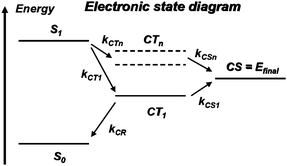 | ||
| Fig. 4 Electronic state diagram. S0 denotes the singlet ground state of the donor or the acceptor and S1, the first singlet excited state reached after optical excitation (exciton state); at the D/A interface, intermolecular charge transfer leads to charge-transfer (CT) states where the hole is on donor molecule(s) and the electron on acceptor molecule(s): CT1 is the lowest energy charge-transfer state; the CTn states represent higher-energy, more diffuse charge-transfer states; the final state relevant for photovoltaics operation is a charge-separated state (CS) where the hole in the donor layer and the electron in the acceptor layer have become free from one another; the ki terms indicate competing transfer rates between various electronic states. | ||
In most instances, the dissociation process is described as involving a transition from the exciton state down to the lowest CT state, which corresponds to the situation where the hole sits on the HOMO level of a D molecule and the electron on the LUMO level of an adjacent A molecule (see Fig. 4). However, in such a case, since they remain in close proximity, the electron and the hole are still rather strongly Coulombically bound, which is precisely the reason why that CT state is lowest in energy. Several scenarios have been proposed to explain the eventual separation of the charges from the lowest CT state, for instance, the presence of disorder or dipoles at the interface or the assistance of phonons,62,63 which would make the kCS1 charge-separation rate larger than the kCR charge-recombination rate.
Another proposition has been recently advanced.64 It involves the efficient coupling of the exciton arriving at the interface to higher-lying CTn states. By definition, such states are more diffuse than the lowest CT state and could be delocalized over a few sites; as a result, the electron and the hole could become more distant and more easily screened from one another, which would lead to easier charge separation. For that process to be relevant, the kCTn and kCSn rates have to be larger than those bringing the system down to CT1.
Note that many factors can complicate the description of the D/A interfacial processes. Suppose that the exciton reaching the interface has formed in the donor. First, instead of direct electron transfer from D to A, there could occur energy transfer leading to the formation of an exciton on A, followed by hole transfer from A to D; this process has been demonstrated in the case of oligophenylene-fullerene dyads.65 The final state is the same as for the direct electron-transfer process; however, the rates involved in the energy-transfer and hole-transfer processes can be markedly different. Secondly, even when singlet excitons are exclusively formed in D, triplet excitons can appear at the interface. For instance in bis-dicyanovinyl-oligothiophenes/fullerene blends, it has been observed66 that, for certain thiophene oligomer lengths, excitons can efficiently transfer to C60 where the large intersystem crossing leads to the formation of triplet excitons, which then hop back to the donor; such processes do not result in charge separation and constitute a loss mechanism.
Thus, the situation is much more complex than what the simple HOMO-LUMO diagrams often found in the literature (and illustrated in Fig. 3c) would lead one to believe. In addition, charge separation can also be influenced by concentration and morphology gradients near the heterojunction that take place during the formation of the organic films, or can be assisted by local electric fields.67 New theoretical methodologies are being developed to provide better descriptions and understanding of all these competing mechanisms.
Charge carrier mobility and collection at electrodes
Once the charges have separated, they can drift and diffuse towards their respective electrodes with efficiency depending on their mobilities. Because of the large electron-vibration coupling in π-conjugated materials and of disorder effects, each charge is associated to a local geometry relaxation and constitutes a polaron (radical-ion in chemical terminology) which hops from molecule to molecule.68 The corresponding polaronic electronic state has an energy defined by the (adiabatic) ionization potential (IP) of the donor or electron affinity (EA) of the acceptor (note that in the simple HOMO–LUMO diagrams, Efinal would be crudely approximated by the difference between the energies of the donor HOMO and acceptor LUMO). The sum of the energies of the polaron states for the donor and acceptor, Efinal = IP(D) + EA(A), represents the energy of the final state of the system, see Fig. 4. To a large extent, Efinal defines the upper limit for the open-circuit voltage of the solar cell, as discussed below.The nature of the electrode/organic layer interfaces is complex. The efficiency of the charge collection process cannot be simply determined from the difference between the workfunction of the isolated electrode and the donor IP or acceptor EA. The deposition of organic layers on electrodes (or vice versa) lead to interfacial charge-density redistributions and/or geometry modifications that strongly affect the alignment of the organic frontier electronic levels vs. the electrode Fermi level.38 Much remains to be done to understand the intricate details of these interfaces. Surface modification of the electrodesvia deposition of self-assembled monolayers69 is an efficient way to enhance the quality of the electrical contact as well as, in particular when dealing with conducting oxide electrodes, to promote compatibilization between the (hydrophilic) oxide surface and (hydrophobic) organic layer.
Device performance and modeling
Here, we discuss the electrical characteristics of organic solar cells and their performance. In the dark the solar cell works as a diode. As for conventional p–n solar cells, an organic photovoltaic device can be approximated by an equivalent circuit, see Fig. 5d, comprised of: (i) a diode with reverse saturation current density J0 (current density in the dark at reverse bias) and ideality factor n; (ii) a current source (Jph), which corresponds to the photocurrent upon illumination; (iii) a series resistance (RS), which has to be minimized and takes account of the finite conductivity of the semiconducting material, the contact resistance between the semiconductors and the adjacent electrodes, and the resistance associated with electrodes and interconnections; and (iv) a shunt (RP) resistance, which needs to be maximized and takes into account the loss of carriers via possible leakage paths; the latter include structural defects such as pinholes in the film, or recombination centers introduced by impurities. Solving for this simple circuit provides the following analytical expression for the current–voltage characteristics, referred to as the Shockley equation:3–5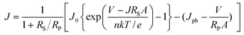 | (1) |
 | (2) |
 | (3) |
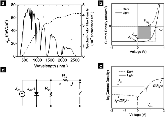 | ||
| Fig. 5 Optical and electrical properties of solar cells. (a) Spectral photon flux density in the standardized AM 1.5 G illumination conditions and corresponding integrated current that would be produced if each photon contributes to current with unity efficiency. (b) Current–density voltage characteristics of a solar cell in the dark and under illumination. (c) Semi-logarithmic plot of the same electrical characteristics, illustrating the effects of the parasitic resistances RS and RP in forward and reverse bias. (d) Equivalent circuit used to model solar cells. The notations are defined in the text. | ||
Eqns (1)–(3) usually need to be solved numerically except for cases where RS is very small and/or RP sufficiently large so that the effect of RS or RP can be ignored; in such instances, the approximate expressions on the right hand side of eqns (2)–(3) apply. When the device is under illumination, two quantities can be easily determined experimentally: the intersects of the electrical characteristics with the vertical and horizontal axes, which correspond to JSC and VOC, respectively (see Fig. 5b). At any point on the electrical characteristic in the fourth quadrant (JSC negative and VOC positive), the solar cell produces an electrical power density given by the product of voltage and current density. This product is maximized at a point that corresponds to voltage Vmax and current density Jmax. The power conversion efficiency η, which represents the most important metric for a photovoltaic cell, is then defined as:
 | (4) |
Fill factor
The maximum value for the fill factor is a function of the open-circuit voltage VOC and the ideality factor of the diode n (optimally equal to 1). As for inorganic solar cells based on p–n junctions, its maximum value can be described by the empirical expression:3 | (5) |
Short-circuit current density
The maximum JSC is given by: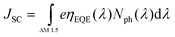 | (6) |
Open-circuit voltage
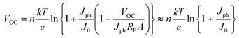
As in the case of conventional solar cells, maximization of the short-circuit current density by using organic semiconductors with decreasing optical absorption gap is not overall an effective strategy since the maximum open-circuit voltage presents an opposite trend with optical absorption gap. It follows that the determination of the optimum light-harvesting conditions to maximize the efficiency of organic solar cells depends largely on the understanding of the origin of VOC and its dependence on materials properties, in particular the relative energies of the relevant energy levels at the organic heterojunction.Neglecting the effects of the parasitic resistances, according to eqn (2), VOC is a logarithmic function of the ratio of the short-circuit current and the reverse saturation current. In the dark, in the absence of carriers, the device is in equilibrium and no photovoltage or VOC is observed since the dark J–V characteristics cross the origin. Upon illumination, absorbed photons generate charge carriers, whose distributions can be described by non-equilibrium quasi-Fermi levels (see Fig. 2a). For illumination levels such that the produced photocurrent is larger than the reverse saturation current (which holds true under average illumination conditions), VOC is observed experimentally to increase logarithmically with intensity. Since the maximum short-circuit current can be estimated using eqn (6), reaching the maximum VOC value requires that the reverse saturation current density J0 be kept at a minimum. Recent studies by Scharber and co-workers78 on bulk heterojunction cells and Rand and co-workers79 on multilayer solar cells, indicate that VOC in organic solar cells depends on the energy difference between the ionization potential of the D component and the electron affinity of the A component forming the heterojunction. Studies of the temperature dependence of the reverse saturation current J0 by Waldauf et al.80 in bulk heterojunctions and Rand79 in multilayer structures of small molecules, show that the reverse saturation current can be approximated by:
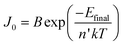 | (7) |
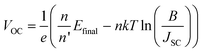 | (8) |
From the energy diagram in Fig. 2b, Efinal = IP(D) + EA(A) is increased as the energy offsets Δ between the D and A molecular states are decreased. However, too strong a reduction in Δ compromises the efficiency of exciton dissociation at the heterojunction and thus decreases the photocurrent; it is generally accepted that Δ has to be on the order of ∼0.3–0.5 eV to overcome the exciton binding energy. In this case, optimized conditions to maximize the power conversion efficiency in an organic single heterojunction cell are obtained for a band gap in the range EG = 1.6–1.9 eV (775–650 nm).
It is worth mentioning that molecules with EA energies larger than 4.2 eV are less sensitive to oxidation in the presence of oxygen and moisture.81 Hence, optimized material combinations should not only satisfy conditions associated with relative state energies but also absolute energies referenced to the vacuum level.
Based on this analysis, a limit of the maximum power efficiency of an idealized single junction organic solar cell can be estimated. With an optimized optical band gap of EG = 1.6 eV (775 nm) and a hypothetical average external quantum efficiency of ηEQE = 0.8, a maximum short-circuit current of JSC,max = 20.2 mA cm−2 is calculated from eqn (6) (see also Fig. 5a). A required energy offset of Δ = 0.5 eV would translate into Efinal = IP(D) + EA(A) = EG − Δ = 1.1 eV. From eqn (8) and assuming that the solar cell has an ideality factor of n = 1.5 and with n′ ≈ n, the maximum open-circuit voltage is estimated to be VOC,max = 0.68 V. Such a VOC,max leads to a normalized voltage VOC = eVOC/nkT= 17.4 V, from which, according to eqn (5), an ideal maximum fill factor FF0 = 0.79 is obtained. Following eqn (4), these values translate into a power conversion efficiency η = 10.8%. Table 1 collects a summary of these estimates and provides examples of parameters measured in solar cells fabricated from different materials.
| Device type | J SC/mA cm−2 | V OC/V | FF | PCEc (%) | Reference |
|---|---|---|---|---|---|
| a PERL: passivated emitter, rear locally diffused; fabricated from high quality fusion zone (FZ) monocrystalline silicon substrates. b Triple junction cell. c PCE: Power conversion efficiency. | |||||
| Monocrystalline Si PERLacell | 42.2 | 0.706 | 0.828 | 24.7 | 82 |
| Multicrystalline Si cell | 35.6 | 0.631 | 0.808 | 18.2 | 83 |
| Monocrystalline Si commercial module | — | — | — | 16.9 | SunPower |
| a-Si cell b | 8.11 | 2.297 | 0.697 | 13.0 | 84 |
| a-Si commercial module | — | — | — | 6.3 | United Solar |
| CdTe cell | 26.08 | 0.840 | 0.731 | 16.0 | 10 |
| CIGS cell | 35.7 | 0.689 | 0.781 | 19.2 | 9 |
| Grätzel cell | 20.53 | 0.721 | 0.704 | 10.4 | 85 |
| Nanocrystal hybrid cell | 13.2 | 0.45 | 0.49 | 2.9 | 24 |
| OPV: 1986 Tang cell | 2.3 | 0.45 | 0.65 | 0.9 | 16 |
| OPV: Small molecule cell | 15.4 | 0.50 | 0.46 | 3.5 | 45 |
| OPV: P3HT:PCBM single cell | 9.5 | 0.63 | 0.68 | 5.1 | 56 |
| OPV tandem cell | 7.8 | 1.24 | 0.67 | 6.5 | 76 |
| Ideal single heterojunction OPV cell | 20.2 | 0.68 | 0.79 | 10.8 | See text |
Future prospects and challenges
The future of organic solar cells as a pervasive technology for portable power will largely rely on their economic potential.86 This depends on a number of intricate factors such as efficiency, manufacturing cost, lifetime, form factor, weight, scalability, and sustainable manufacturing. At this point, two main manufacturing techniques can be foreseen, vacuum processing and wet processing. Vacuum processing presents the advantages of relatively easy fabrication of, on one hand, high-quality thin films from highly purified materials with well-controlled thickness and, on the other hand, devices with complex multilayer architectures. The limiting factors are the deposition rates and the tooling costs associated with vacuum techniques. Wet processing allows for high throughputs using various printing techniques and holds the long-term promise of lowest manufacturing costs. However, printing of organic semiconductors into pinhole-free and 100 nm-thick films over large areas remains a major challenge. Semiconductor inks generally have low viscosity which limits the range of adequate printing techniques. Furthermore, substrates and electrodes have surface energies that are significantly different from those of organic semiconductor inks, which can lead to wetting issues. Vertical segregation87 and other rheological effects also make it difficult to control the nanoscale phase-separated morphology88 necessary for good operation of bulk heterojunctions. Stability of the inks after formulation is another challenge that vacuum processing does not face.A cost factor common to all material platforms is packaging. Coatings with small transmission rates to oxygen and moisture are necessary to protect the organic semiconductors from undergoing photo-oxidative reactions that limits their stability over time. Packaging techniques must be compatible with the substrate and active materials89 and keep the overall manufacturing cost low. Since highly flexible form factors are possible, much work remains to be done to understand how flexing affects the operation of the devices and their packaging. Most laboratory cells with efficiencies in the range of 2–6% have been fabricated over small areas, and area scaling without loss of efficiency is required. A clear advantage of organics over crystalline silicon is the relative ease of monolithic integration,90 which reduces the module assembly cost considerably.
If organic photovoltaic technologies mature beyond niche consumer market applications and become players in power generation, their composition must be based on materials available on large scales at low cost. Also, concerns about the limited supply of indium ($900 per kg) are currently fueling research efforts to replace ITO as the transparent electrode.91–93 Promising results have been demonstrated, for instance, with polymers doped with carbon nanotubes.
Last but not least, organic solar cells must demonstrate lifetimes of several years. While organic cells might not show twenty years of operational lifetime like crystalline silicon cells, the recent demonstration of 100![[thin space (1/6-em)]](https://www.rsc.org/images/entities/char_2009.gif) 000 h operational lifetime in organic light-emitting diodes is indicative that long lifetimes are within reach with organic semiconductors.
000 h operational lifetime in organic light-emitting diodes is indicative that long lifetimes are within reach with organic semiconductors.
To summarize, organic photovoltaics provides an exciting playground at the frontiers of science, engineering, and technology. Advances in the near term are likely to lead to solar cells with efficiencies close to 10% in single heterojunction geometries and efficiencies up to 15% in tandem-cell geometries. If organic photovoltaics holds its promise, it can soon become an ubiquitous, clean and sustainable technology for portable power and potentially provide large-scale energy production for future generations.
Acknowledgements
This material is based upon work supported in part by the STC Program of the National Science Foundation under Agreement Number DMR-0120967, the Office of Naval Research, the Department of Energy, the Georgia Research Alliance, and the AtlanTICC Alliance.References
- E. Becquerel, Mémoire sur les effets électriques produits sous l'influence des rayons solaires, C. R. Acad. Sci., 1839, 9, 561–567 Search PubMed.
- D. M. Chapin, C. S. Fuller and G. L. Pearson, A new silicon p-n junction photocell for converting solar radiation into electrical power, J. Appl. Phys., 1954, 25, 676 CAS.
- M. A. Green, Solar Cells, The University of New South Wales, Kensington, Australia, 1998 Search PubMed.
- P. Wurfel, Physics of Solar Cells, Wiley VCH, Weinheim, Germany, 2005 Search PubMed.
- R. H. Bube, Photovoltaic Materials, Imperial College Press, London, UK, 1998 Search PubMed.
- For general information about solar energy, consult the International Energy Agency Photovoltaic Power Systems Program at http://www.iea-pvps.org.
- S. Hegedus, Thin film solar modules: The low cost, high throughput and versatile alternative to Si wafers, Prog. Photovoltaics, 2006, 14, 393–411 CAS.
- A. Slaoui and R. T. Collins, Advanced inorganic materials for photovoltaics, MRS Bull., 2007, 32, 211.
- K. Ramanathan et al., Properties of 19.2% efficiency ZnO/CdS/CuInGaSe2 thin-film solar cells, Prog. Photovoltaics, 2003, 11, 225.
- T. Aramoto et al., 16.0% efficient thin-film CdS/CdTe solar cells, Jpn. J. Appl. Phys., Part 1, 1997, 36, 6304 CrossRef.
- R. H. Friend et al., Electroluminescence in conjugated polymers, Nature, 1999, 397, 121 CrossRef CAS.
- F. Garnier, R. Hajlaoui, A. Yassar and P. Srivastava, All-polymer field-effect transistor realized by printing techniques, Science, 1994, 265, 1684.
- C. D. Dimitrakopoulos and P. R. L. Malenfant, Organic thin film transistors for large area electronics, Adv. Mater., 2002, 14, 99 CrossRef CAS.
- P. Peumans, A. Yakimov and S. R. Forrest, Small molecular weight organic thin-film photodetectors and solar cells, J. Appl. Phys., 2003, 93, 3693 CrossRef CAS.
- M. Pope and C. E. Swenberg, Electronic Processes in Organic Crystals and Polymers, Oxford University Press, New York, 1999 Search PubMed.
- C. W. Tang, Two-layer organic photovoltaic cell, Appl. Phys. Lett., 1986, 48, 183 CrossRef CAS.
- D. Kearns and M. Calvin, Photovoltaic effect and photoconductivity in organic laminated systems, J. Chem. Phys., 1958, 29, 950–951 CrossRef CAS.
- G. Yu, J. Gao, J. C. Hummelen, F. Wudl and A. J. Heeger, Polymer photovoltaic cells – enhanced efficiencies via a network of internal donor–acceptor heterojunctions, Science, 1995, 270, 1789 CrossRef CAS.
- J. J. M. Halls et al., Efficient photodiodes from interpenetrating polymer networks, Nature, 1995, 376, 498 CrossRef CAS.
- M. Grätzel, Photoelectrochemical cells, Nature, 2001, 414, 338 CrossRef CAS.
- M. K. Nazeeruddin et al., Conversion of light to electricity by cis-x2bis(2,2′-bipyridyl-4,4′-dicarboxylate)ruthenium(II) charge-transfer sensitizers (x = Cl−, Br−, I−, CN−, and SCN−) on nanocrystalline TiO2 electrodes, J. Am. Chem. Soc., 1993, 115, 6382 CrossRef CAS.
- F. Dimroth and S. Kurtz, High-efficiency multijunction solar cells, MRS Bull., 2007, 32, 230 CAS.
- W. U. Huynh, J. J. Dittmer and A. P. Alivisatos, Hybrid nanorod-polymer solar cells, Science, 2002, 295, 2425 CrossRef CAS.
- I. Gur, N. A. Fromer, M. L. Geier and A. P. Alivisatos, Air-stable all-inorganic nanocrystal solar cells processed from solution, Science, 2005, 310, 462 CrossRef CAS.
- D. J. Milliron, I. Gur and A. P. Alivisatos, Hybrid organic–nanocrystal solar cells, MRS Bull., 2005, 30, 41 CAS.
- A. Petrella et al., Colloidal TiO2 nanocrystals/MEH:PPV nanocomposites: Photo(electro)chemical study, J. Phys. Chem. B, 2005, 109, 1554 CrossRef CAS.
- K. Sayama et al., Efficient sensitization of nanocrystalline TiO2 films with cyanine and merocyanine organic dyes, Sol. Energy Mater. Sol. Cells, 2003, 80, 47 CrossRef CAS.
- A. C. Arango et al., Efficient titanium oxide/conjugated polymer photovoltaics for solar energy conversion, Adv. Mater., 2000, 12, 1689 CrossRef CAS.
- K. M. Coakley, Y. X. Liu, C. Goh and M. D. McGehee, Ordered organic-inorganic bulk heterojunction photovoltaic cells, MRS Bull., 2005, 30, 37 CAS.
- K. M. Coakley, Y. X. Liu, M. D. McGehee, K. L. Frindell and G. D. Stucky, Infiltrating semiconducting polymers into self-assembled mesoporous titania films for photovoltaic applications, Adv. Funct. Mater., 2003, 13, 301 CrossRef CAS.
- J. L. Brédas, J. Cornil and A. J. Heeger, The exciton binding energy in luminescent conjugated polymers, Adv. Mater., 1996, 8, 447 CAS.
- S. F. Alvarado, P. F. Seidler, D. G. Lidzey and D. D. C. Bradley, Direct determination of the exciton binding energy of conjugated polymers using a scanning tunneling microscope, Phys. Rev. Lett., 1998, 81, 1082 CrossRef CAS.
- J. Nelson, Organic photovoltaic films, Curr. Opin. Solid State Mater. Sci., 2002, 6, 87 CrossRef CAS.
- Organic Photovoltaics: Mechanisms, Materials and Devices, ed. S. S. Sun and N. S. Sariciftci, Taylor and Francis, Boca Raton, FL, 2005 Search PubMed.
- S. E. Shaheen, D. S. Ginley and G. E. Jabbour, Organic-based photovoltaics. Toward lowm-cost power generation, MRS Bull., 2005, 30, 10 CAS.
- H. Hoppe and N. S. Sariciftci, Organic solar cells: An overview, J. Mater. Res., 2004, 19, 1924 CAS.
- H. Spanggaard and F. C. Krebs, A brief history of the development of organic and polymeric photovoltaics, Sol. Energy Mater. Sol. Cells, 2004, 83, 125 CrossRef CAS.
- V. Coropceanu et al., Charge transport in organic semiconductors, Chem. Rev., 2007, 107, 926 CrossRef CAS.
- Conjugated Polymers and Molecular Interfaces, ed. W. R. Salaneck, K. Seki, A. Kahn and J.-J. Pireaux, Marcel Dekker, New York, 2002 Search PubMed.
- R. F. Pierret Semiconductor Device Fundamentals, Addison Wesley, Reading, Massachusetts, 1996 Search PubMed.
- S. M. Sze and K. K. Ng, Physics of Semiconductor Devices, Wiley Interscience, Hoboken, New Jersey, 2007 Search PubMed.
- I. H. Campbell, T. W. Hagler, D. L. Smith and J. P. Ferraris, Direct measurement of conjugated polymer electronic excitation energies using metal/polymer/metal structures, Phys. Rev. Lett., 1996, 76, 1900 CrossRef CAS.
- P. W. M. Blom, V. D. Mihailetchi, L. J. A. Koster and D. E. Markov, Device physics of polymer: Fullerene bulk heterojunction solar cells, Adv. Mater., 2007, 19, 1551 CrossRef CAS.
- S. Yoo, B. Domercq and B. Kippelen, Efficient thin-film organic solar cells based on pentacene/C60 heterojunctions, Appl. Phys. Lett., 2004, 85, 5427 CrossRef CAS.
- S. Uchida, J. G. Xue, B. P. Rand and S. R. Forrest, Organic small molecule solar cells with a homogeneously mixed copper phthalocyanine:C60 active layer, Appl. Phys. Lett., 2004, 84, 4218 CrossRef CAS.
- P. Peumans, S. Uchida and S. R. Forrest, Efficient bulk heterojunction photovoltaic cells using small-molecular-weight organic thin films, Nature, 2003, 425, 158 CrossRef CAS.
- J. Drechsel et al., Efficient organic solar cells based on a double p-i-n architecture using doped wide-gap transport layers, Appl. Phys. Lett., 2005, 86, 244102 CrossRef.
- F. Yang, M. Shtein and S. R. Forrest, Controlled growth of a molecular bulk heterojunction photovoltaic cell, Nat. Mater., 2005, 4, 37 CrossRef CAS.
- A. K. Pandey, S. Dabos-Seignon and J. M. Nunzi, Pentacene: PTCDI-C13H27 molecular blends efficiently harvest light for solar cell applications, Appl. Phys. Lett., 2006, 89 Search PubMed.
- K. Suemori, T. Miyata, M. Yokoyama and M. Hiramoto, Three-layered organic solar cells incorporating a nanostructure-optimized phthalocyanine:fullerene codeposited interlayer, Appl. Phys. Lett., 2005, 86 Search PubMed.
- B. Maennig et al., Organic p-i-n solar cells, Appl. Phys. A, 2004, 79, 1 CrossRef CAS.
- M. Hiramoto, H. Fujiwara and M. Yokoyama, 3-layered organic solar-cell with a photoactive interlayer of codeposited pigments, Appl. Phys. Lett., 1991, 58, 1062 CrossRef CAS.
- E. Moons, Conjugated polymer blends: Linking film morphology to performance of light emitting diodes and photodiodes, J. Phys.: Condens. Matter, 2002, 14, 12235 CrossRef CAS.
- F. Padinger, R. S. Rittberger and N. S. Sariciftci, Effects of postproduction treatment on plastic solar cells, Adv. Funct. Mater., 2003, 13, 85 CrossRef CAS.
- J. Peet et al., Efficiency enhancement in low-bandgap polymer solar cells by processing with alkane dithiols, Nat. Mater., 2007, 6, 497 CrossRef CAS.
- W. L. Ma, C. Y. Yang, X. Gong, K. Lee and A. J. Heeger, Thermally stable, efficient polymer solar cells with nanoscale control of the interpenetrating network morphology, Adv. Funct. Mater., 2005, 15, 1617 CrossRef CAS.
- G. Li et al., High-efficiency solution processable polymer photovoltaic cells by self-organization of polymer blends, Nat. Mater., 2005, 4, 864 CAS.
- L. Salem, The Molecular Orbital Theory of Conjugated Systems, Benjamin, New York, 1966 Search PubMed.
- L. A. A. Pettersson, L. S. Roman and O. Inganas, Modeling photocurrent action spectra of photovoltaic devices based on organic thin films, J. Appl. Phys., 1999, 86, 487 CrossRef CAS.
- J. Gilot, I. Barbu, M. M. Wienk and R. A. J. Janssen, The use of ZnO as optical spacer in polymer solar cells: Theoretical and experimental study, Appl. Phys. Lett., 2007, 91, 113520 CrossRef.
- H. Wiesenhofer et al., Limitations of the Förster description of singlet exciton migration: The illustrative example of energy transfer to ketonic defects in ladder-type poly(para-phenylenes), Adv. Funct. Mater., 2005, 15, 155 CrossRef.
- V. I. Arkhipov, P. Heremans and H. Bassler, Why is exciton dissociation so efficient at the interface between a conjugated polymer and an electron acceptor?, Appl. Phys. Lett., 2003, 82, 4605 CrossRef CAS.
- T. Offermans, S. C. J. Meskers and R. A. J. Janssen, Charge recombination in a poly(para-phenylene vinylene)-fullerene derivative composite film studied by transient, nonresonant, hole-burning spectroscopy, J. Chem. Phys., 2003, 119, 10924 CrossRef CAS.
- A. C. Morteani, P. Sreearunothai, L. M. Herz, R. H. Friend and C. Silva, Exciton regeneration at polymeric semiconductor heterojunctions, Phys. Rev. Lett., 2004, 92, 247402 CrossRef.
- E. Peeters et al., Synthesis, photophysical properties, and photovoltaic devices of oligo(p-phenylene vinylene)-fullerene dyads, J. Phys. Chem. B, 2000, 104, 10174 CrossRef CAS.
- R. Schueppel et al., Enhanced photogeneration of triplet excitons in an oligothiophene fullerene blend, ChemPhysChem, 2007, 8, 1497 CrossRef.
- M. Koeler, M. C. Santos and M. G. E. da Luz, Positional disorder enhancement of exciton dissociation at donor/acceptor interface, J. Appl. Phys., 2006, 99, 053702 CrossRef.
- G. Heimel et al., Toward control of the metal-organic interfacial electronic structure in molecular electronics: A first-principles study on self-assembled monolayers of pi-conjugated molecules on noble metals, Nano Lett., 2007, 7, 932 CrossRef.
- S. Khodabakhsh, B. M. Sanderson, J. Nelson and T. S. Jones, Using self-assembling dipole molecules to improve charge collection in molecular solar cells, Adv. Funct. Mater., 2006, 16, 95 CrossRef CAS.
- M. Hiramoto, M. Suezaki and M. Yokoyama, Effect of thin gold interstitial-layer on the photovoltaic properties of tandem organic solar-cells, Chem. Lett., 1990, 327 Search PubMed.
- B. P. Rand, P. Peumans and S. R. Forrest, Long-range absorption enhancement in organic tandem thin-film solar cells containing silver nanoclusters, J. Appl. Phys., 2004, 96, 7519 CrossRef CAS.
- J. G. Xue, S. Uchida, B. P. Rand and S. R. Forrest, Asymmetric tandem organic photovoltaic cells with hybrid planar-mixed molecular heterojunctions, Appl. Phys. Lett., 2004, 85, 5757 CrossRef CAS.
- A. Hadipour, B. de Boer and P. W. M. Blom, Solution-processed organic tandem solar cells with embedded optical spacers, J. Appl. Phys., 2007, 102 Search PubMed 074506.
- J. Gilot, M. M. Wienk and R. A. J. Janssen, Double and triple junction polymer solar cells processed from solution, Appl. Phys. Lett., 2007, 90, 143512 CrossRef.
- A. G. F. Janssen, T. Riedl, S. Hamwi, H. H. Johannes and W. Kowalsky, Highly efficient organic tandem solar cells using an improved connecting architecture, Appl. Phys. Lett., 2007, 91 Search PubMed 073519.
- J. Y. Kim et al., Efficient tandem polymer solar cells fabricated by all-solution processing, Science, 2007, 317, 222 CrossRef CAS.
- K. Tvingstedt, V. Andersson, F. Zhang and O. Inganas, Folded reflective tandem polymer solar cell doubles efficiency, Appl. Phys. Lett., 2007, 91, 123514 CrossRef.
- M. C. Scharber et al., Design rules for donors in bulk-heterojunction solar cells - towards 10 % energy-conversion efficiency, Adv. Mater., 2006, 18, 789 CrossRef CAS.
- B. P. Rand, D. P. Burk and S. R. Forrest, Offset energies at organic semiconductor heterojunctions and their influence on the open-circuit voltage of thin-film solar cells, Phys. Rev. B, 2007, 75, 115327 CrossRef.
- C. Waldauf, M. C. Scharber, P. Schilinsky, J. A. Hauch and C. J. Brabec, Physics of organic bulk heterojunction devices for photovoltaic applications, J. Appl. Phys., 2006, 99, 104503 CrossRef.
- D. M. De Leeuw, M. M. J. Simenon, A. R. Brown and R. E. F. Einerhand, Stability of n-type doped conducting polymers and consequences for polymeric microelectronic devices, Synth. Met., 1997, 87, 53 CrossRef.
- J. H. Zhao, A. H. Wang and M. A. Green, 24.5% efficiency silicon PERT cells on MCZ substrates and 24.7% efficiency PERL cells on FZ substrates, Prog. Photovoltaics, 1999, 7, 471 CAS.
- A. Rohatgi, S. Narasimha, S. Kamra and C. P. Khattak, Fabrication and analysis of record high 18.2% efficient solar cells on multicrystalline silicon material, IEEE Electron Device Lett., 1996, 17, 401 CrossRef CAS.
- J. Yang, A. Banerjee and S. Guha, Triple-junction amorphous silicon alloy solar cell with 14.6% initial and 13.0% stable conversion efficiencies, Appl. Phys. Lett., 1997, 70, 2975 CrossRef CAS.
- M. K. Nazeeruddin et al., Engineering of efficient panchromatic sensitizers for nanocrystalline TiO2-based solar cells, J. Am. Chem. Soc., 2001, 123, 1613 CrossRef CAS.
- C. J. Brabec, J. A. Hauch, P. Schilinsky and C. Waldauf, Production aspects of organic photovoltaics and their impact on the commercialization of devices, MRS Bull., 2005, 30, 50.
- A. C. Arias, Vertically segregated polymer blends: Their use in organic electronics, Polym. Rev., 2006, 46, 103 Search PubMed.
- J. S. Huang et al., Investigation of the effects of doping and post-deposition treatments on the conductivity, morphology, and work function of poly (3,4-ethylenedioxythiophene)/poly (styrene sulfonate) films, Adv. Funct. Mater., 2005, 15, 290 CrossRef CAS.
- W. J. Potscavage, S. Yoo, B. Domercq and B. Kippelen, Encapsulation of pentacene/C60 organic solar cells with Al2O3 deposited by atomic layer deposition, Appl. Phys. Lett., 2007, 90, 253511 CrossRef.
- S. Yoo et al., Integrated organic photovoltaic modules with a scalable voltage output, Appl. Phys. Lett., 2006, 89, 233516 CrossRef.
- J. van de Lagemaat et al., Organic solar cells with carbon nanotubes replacing In2O3:Sn as the transparent electrode, Appl. Phys. Lett., 2006, 88, 233503 CrossRef.
- M. W. Rowell et al., Organic solar cells with carbon nanotube network electrodes, Appl. Phys. Lett., 2006, 88, 233506 CrossRef.
- A. D. Pasquier, H. E. Unalan, A. Kanwal, S. Miller and M. Chhowalla, Conducting and transparent single-wall carbon nanotube electrodes for polymer-fullerene solar cells, Appl. Phys. Lett., 2005, 87, 203511 CrossRef.
| This journal is © The Royal Society of Chemistry 2009 |