III–V multijunction solar cells for concentrating photovoltaics
Hector
Cotal
,
Chris
Fetzer
,
Joseph
Boisvert
,
Geoffrey
Kinsey
,
Richard
King
,
Peter
Hebert
,
Hojun
Yoon
and
Nasser
Karam
Spectrolab, Inc, Sylmar, California 91342, USA
First published on 10th December 2008
Abstract
Concerns about the changing environment and fossil fuel depletion have prompted much controversy and scrutiny. One way to address these issues is to use concentrating photovoltaics (CPV) as an alternate source for energy production. Multijunction solar cells built from III–V semiconductors are being evaluated globally in CPV systems designed to supplement electricity generation for utility companies. The high efficiency of III–V multijunction concentrator cells, with demonstrated efficiency over 40% since 2006, strongly reduces the cost of CPV systems, and makes III–V multijunction cells the technology of choice for most concentrator systems today. In designing multijunction cells, consideration must be given to the epitaxial growth of structures so that the lattice parameter between material systems is compatible for enhancing device performance. Low resistance metal contacts are crucial for attaining high performance. Optimization of the front metal grid pattern is required to maximize light absorption and minimize I2R losses in the gridlines and the semiconductor sheet. Understanding how a multijunction device works is important for the design of next-generation high efficiency solar cells, which need to operate in the 45%–50% range for a CPV system to make better economical sense. However, the survivability of solar cells in the field is of chief concern, and accelerated tests must be conducted to assess the reliability of devices during operation in CPV systems. These topics are the focus of this review.
 Hector Cotal Hector Cotal | Dr Cotal received his PhD in Solid State Physics from Oklahoma State University. As a Postdoctoral Fellow he worked on InP-, GaAs- and Si-based solar cells at the Naval Research Laboratory. He leads Spectrolab's terrestrial development programs for the design, fabrication and testing of III–V multijunction solar cells. His interests are in device physics, device and heat transfer modeling, SMT of concentrator cells and terrestrial PV designs for use in specialized applications. He won R&D 100 (2001 & 2007) and Scientific American 50 (2002) recognition for his outstanding work in the development of the Triple Junction Terrestrial Concentrator Solar Cell Technology. |
 Chris Fetzer Chris Fetzer | Dr Fetzer is manager of the MOVPE research and development group responsible for the development of metal–organic vapor phase epitaxial deposition processes for advanced solar cells and photonic devices. He received his BS in Physics and PhD in Materials Science and Engineering from University of Utah. As an Associate Technical Fellow at the Boeing Company he has developed advanced epitaxial layers of III–V compound semiconductors. Before joining Spectrolab in 2001, Dr Fetzer performed research under Dr G. B. Stringfellow at the University of Utah exploring the use of surfactant-mediated epitaxy to control ternary alloy microstructure and the underlying surface physics. |
 Joseph Boisvert Joseph Boisvert | Joseph Boisvert was born in Malden, Massachusetts. He received his BS from the Massachusetts Institute of Technology in 1980 and MS and PhD degrees from the University of Illinois at Urbana-Champaign in 1984. Dr Boisvert is presently a Senior Scientist/Engineer at Spectrolab, Inc., a Boeing Company, where he is responsible for developing III–V photodetectors and solar cells. He has 24 years of experience in the research and development of solid-state photodetectors and solar cells, including device and process design, modeling, test and data analysis. Dr. Boisvert is an Associate Technical Fellow of the Boeing Company. |
 Richard King Richard King | Dr Richard R. King is Boeing Technical Fellow and Principal Scientist responsible for Photovoltaic Cell R&D at Spectrolab. He received his BS, MS and PhD degrees at Stanford University. His photovoltaics research over the last 20 years includes work on III–V metamorphic materials and devices, 4-, 5-, and 6-junction cells, and minority-carrier recombination at heterointerfaces. Dr King led Spectrolab's development of high-efficiency III–V multijunction cells, resulting in the first solar cells of any type to reach over 40% efficiency, and was recognized with R&D 100 awards in 2001 and 2007, and a Scientific American 50 award in 2002. Dr King was inducted into the Space Technology Hall of Fame in 2004, and has 11 patents and over 90 publications on photovoltaics and device physics. |
 Peter Hebert Peter Hebert | Mr Hebert received his BS in Mechanical Engineering and BA in Philosophy from the University of Notre Dame, and his MS in Mechanical Engineering from Colorado State University. Mr Hebert performed manufacturing energy efficiency audits at the Industrial Assessment Center at Colorado State while performing his research on high speed deposition of CdTe solar cells. Mr Hebert is a Senior Staff Engineer at Spectrolab. He has nine years experience of performing characterization and qualification testing on multijunction space cells and has received four Hughes Technical Excellence Awards, a patent and a trade secret. Mr Hebert is currently leading qualification of the first generation multijunction terrestrial cells. |
 Nasser Karam Nasser Karam | Dr N. H. Karam is Vice President of Advanced Technology Products and has the overall responsibility for Boeing - Spectrolab's internally and externally funded R&D projects. He has over 20 years of experience in materials research, photovoltaic and optoelectronic devices, and MOCVD reactor design. He is currently actively involved in the development of advanced space solar cells through Spectrolab's jointly funded Dual Use Science & Technology program with the Air Force Research Laboratory. Dr Karam and his Advanced Technology Products Team recently won the R&D 100 and the Scientific American 50 awards for contributions in the field of energy generation. |
1 Introduction
The rising cost of producing electricity from fossil fuels is favorably shifting energy production to renewable resources such as solar photovoltaics (PV), for example.1 Increasing advances in solar cell efficiency and lowering cost endeavors, along with clean energy initiatives are the primary factors for the impetus in solar energy production to date. In 2007, the world production of solar cells reached 3.8 GW with Japan being the leading producer.2 The rest of the world with rapidly increasing development capabilities to manufacture solar cells in mass quantities contributed to over 70% of the total PV generated in 2007. Market trends indicate that solar cell manufacturing capacities have been climbing annually at an average greater than 40% over last 10 years with a 50% leap in 2007 compared to the previous year. Ostensibly, growth in the PV industry is projected to continue growing through 2010 including PV installations.Components such as modules, inverter, tracker, installation and other balance of systems (BOS) are what typically define an installed PV system. The burgeoning demand of global PV installations is driven by the factors mentioned above; however, not all solar cells produced each year have in the past been converted to installed PV power. The disparities between PV produced and installed are due to the lack of more aggressive solar Renewable Portfolio Standards, the deficiency of more market incentives, the lack of implementing product and building regulations, and issues with the supply chain of optical components.3–7 Despite this, global PV installations are rising. In 2007, they rose by an average of 46% compared to 2006 with a finishing year-end total in the range of 2287–2826 MW according to various reports with one rendition evident in Fig. 1.8–10 Most of the power came from Europe, demonstrating dominance once again in this area. Over 1300 MW of this, however, was installed in Germany which is still holding a large section of the industry's market share for installed PV. The global cumulative installed PV electricity in 2007 was over 9 GW which is still an insignificant amount when comparing to the estimated total power consumption in the world of 18 TW (1.8 × 10¹⁰ kW).11,12 The total cumulative power from installed, grid-tied, concentrating photovoltaics (CPV) in 2007 was over 1.5 MW mostly based on single crystal silicon (Si) solar cells and multijunction cells from III–V semiconductors.13–18
 | ||
| Fig. 1 Data obtained from tabular format of annual global installations (systems only) by country.9 Values for 2007 are forecasts. | ||
Multijunction solar cells were first introduced by the Research Triangle Institute and by Varian Research Center in the late 1970s to mid 1980s when dual-junction (2-junction) devices were formed from an AlGaAs junction stacked or grown on top of a GaAs junction, and interconnected by a semiconductor tunnel junction.19,20 In the same decade, another tandem device was proposed by the Solar Energy Research Institute (now the National Renewable Energy Laboratory; NREL) that consisted of a GaInP junction formed on top of a GaAs junction both grown on an inactive Ge substrate which formed a 2-junction solar cell.21 Later in the 1990s, changes in the top cell thickness led to record efficiencies for 2-junction and triple junction (3-junction) solar cells with GaInP and GaAs both grown on top of an active Ge bottom cell substrate.22–24 It had long been realized that the high-efficiency structure of multijunction solar cells makes them highly attractive for cost-effective terrestrial concentrator systems, if designed for the terrestrial solar spectrum and the high current densities under concentration. This was demonstrated with a record efficiency terrestrial concentrator cell grown at Spectrolab and processed at NREL, with 32.3% efficiency.25 At this point, the development of new device designs implemented in terrestrial concentrator cells at Spectrolab led to a surge in demonstrated efficiencies,26–29 with an increase of 8 percentage points in absolute efficiency in as many years. This unprecedented rise in demonstrated cell efficiency, as solar cell researchers explored the potential of the multijunction cell design under the concentrated terrestrial spectrum, culminated with a record 40.7% efficient upright metamorphic 3-junction GaInP/GaInAs/Ge concentrator cell,30,31 the first solar cell of any type to reach over the 40% efficiency milestone. In addition to being more efficient than any other solar cell technology, III–V multijunction concentrator solar cells are also the technology for which the efficiency is growing most rapidly. Inverted metamorphic 3-junction cells have now achieved 40.8% efficiency under the standard concentrator terrestrial spectrum.32 Lattice-matched, upright metamorphic, and inverted metamorphic multijunction cell architectures will be discussed in greater detail later in the paper.
Multijunction solar cells in CPV systems offer a low-cost, viable technology for electricity generation. Several experimental systems based on both point focus and dense array configurations have been developed for operation in excess of 400 suns across the world,16,18,33 and the drive to deploy more CPV is on the horizon. In the United States, deployment within the next few years is expected due to the advent of federal- and state-funded solar initiative programs that are currently in progress to enhance the development of CPV technologies.34 These programs will allow the cell conversion efficiency and the PV module efficiency to be pushed to new heights, and will promote costs at the meter as low as US 7–8¢/kWh by 2015.
The boom in the solar PV market has opened the door for CPV. Although over 1.5 MW were installed in 2007, both Boeing Spectrolab and Emcore have acquired large backlog orders to deliver CPV product in the years ahead. Spectrolab has secured deals with Solar Systems PTY, Solfocus and Opel to produce a combined 370 MW of high efficiency 3-junction solar cells. According to press releases, Emcore has also secured deals with Green and Gold Energy, and ES Systems that total 175 MW, and it has also signed a memorandum of understanding with SunPeak Solar to supply 200 to 700 MW of CPV for the utility market.
CPV systems using multijunction solar cells exhibit another benefit. Expensive semiconductor material usage is minimized, which puts a constraint on the system cost components preventing them from getting too high, forcing the size of system parts to be reduced and less expensive. Consider the Si module and the small point-focus CPV module shown in Fig. 2. Fig. 2(a) is a commercial flat plate module populated with 13% polycrystalline silicon solar cells with power rating of 110 W, and active semiconductor area of 62 cm × 152 cm. In contrast, one unit in the concentrator module operates at 500 suns using a 0.55 cm × 0.55 cm multijunction cell with efficiency of 37% as shown in Fig. 2(b). Generating an equivalent power of 110 W in the CPV module is achievable from the following simple calculation: 0.37 × (0.55 cm × 0.55 cm) × 0.75 × N × 50 W cm−2 = 110 W where N is the number of multijunction cells and 0.75 is the optical efficiency of the module. Twenty-six cells (or 7.9 cm2 of semiconductor area) would be required for producing the same power which is 0.084% of the total area of the Si cells.
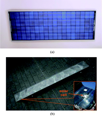 | ||
| Fig. 2 (a) Commercial polycrystalline Si flat plate module. (b) Commercial CPV module using triple junction GaInP/GaInAs/Ge solar cells. The module has 10 individual units each consisting of a solar cell and a secondary optical element as shown in the inset. Printed with permission from SOL3G. | ||
Making CPV systems is attractive for on- and off-grid power generation for the centralized industry, and perhaps distributed applications but the BOS costs; however, add a non-negligible cost element to the overall system. Since raw materials for building the BOS like metals, glasses, and composites have little margin for further cost reduction, other approaches must be contemplated. Increasing cell efficiency and lowering cell costs are great levers in mitigating the system costs as an alternative. Currently, multijunction cells of 37% efficiency cost between $8 and $10/cm2 in large quantities but efforts are underway for further reductions.
More technical advances need to occur for multijunction solar cells to completely overcome cost obstacles and further improve performance in order to trigger the feasibility of low-cost CPV systems. Despite this, significant progress has been made in the development of multijunction solar cells which are now used in their present state in dense array and point focus systems.16,17,35,36 What follows is an account of the latest considerations to make current state-of-the art devices designed to operate at high solar flux. This review begins from the basics of epitaxial device structure followed by a discussion of various device architectures for next-generation high efficiency solar cells. Device physics on ohmic contact formation and device modeling are presented. The principles of solar cell operation under concentrated sunlight are highlighted in some detail with a subsequent discussion of key results. A section that addresses environmental reliability is next, which is a topic that is getting much attention.
2 Device architectures
All the magic of making a modern crystalline III–V multijunction solar cell begins with taking a raw wafer and forming individual layers of crystalline semiconductor on the substrate. This process is known as epitaxy which is a fancy word for crystal growth. There are multiple forms of epitaxial techniques for forming single crystal semiconductor layers. These go by their own acronyms consisting of an alphabet soup of techniques. The oldest is liquid phase epitaxy (LPE) wherein a liquid solution is used for crystallizing layers to a substrate. A good review relating to solar is provided.37 While relatively inexpensive, LPE is limited in producing very sophisticated device structures. The current favored technique is organometallic vapor phase epitaxy (OMVPE) where an organic complex of the semiconductor metals are fed into a reactor vessel containing the wafer. These gasses decompose with the resulting constituent atoms incorporated into crystalline layers upon the substrate atomic template.38,39 There are also a whole host of variants on these techniques, and reviewing each one in depth cannot be easily made in this paper. In general, they are all variants on how delivering atoms to the crystalline substrate take place, and each technique has its individual strengths and weaknesses. A few current techniques are: MBE, MOMBE, ALE, HVPE, etc; all containing an E in the acronym for epitaxy. This is a key feature in that the substrate must be present in forming the crystalline layers. High efficiency multijunction solar cells require true epitaxial growth, not just depositing polycrystalline material as is implied by techniques like chemical vapor-phase deposition (CVD).2.1 Epitaxial device structure
In designing multijunction solar cells, two or more semiconducting layers are stacked as p–n junctions to collect light. In general, they need not be monolithically connected so mechanical stacking of cells is possible. Multijunction solar cells fabricated monolithically, meaning that the semiconductor p–n junctions are epitaxially-grown one upon another, is the topic of this section.A typical 3-junction solar cell structure comprises three n–p junctions made from GaInP, GaInAs and Ge stacked on top of each other—each layer with a band gap energy higher than the layer below it—and assembled with low resistive tunnel junctions. These junctions are formed on a substrate by epitaxial growth techniques to produce a series-connected, monolithically-grown, GaInP/GaInAs/Ge stack. Fig. 3 shows a generalized device structure for a 3-junction solar cell on the left (Fig 3a), and a diagram of the equivalent device electrical circuit on the right (Fig. 3b). The top of the device is the side that points toward the sun. The top p–n junction has the highest band gap energy that collects light from the shortest wavelengths in the solar spectrum. Photons with energy lower than the band gap pass to the lower junction, and photons with energy lower than this threshold traverse to the lowest junction in the stack. The detailed physics of these devices is presented elsewhere.40,41
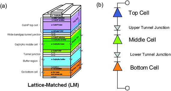 | ||
| Fig. 3 (a) Physical schematic of monolithic triple junction n-on-p solar cell deposited epitaxially upon a substrate. (b) The electrical circuit equivalent diagram showing top, middle and bottom junction diodes and interconnecting upper and lower tunnel junctions. | ||
To fabricate a monolithic device, certain material requirement challenges must be faced. The first of these is that the entire device must be made on the same substrate. In material terminology, the device atomic structures must be similar in atomic spacing and provide the multiple band gaps necessary to produce the junctions. Secondly, high material quality of all layers is necessary for minority carrier electrons and holes to be collected efficiently. The third requirement is that, within the material system, there should be high quality materials that serve as inactive layers to provide the proper dynamics for generated carriers. These layers include front and back surface passivation layers which are typically much higher in band gap than the active layers within the cell. The fourth requirement is that wide ranges in doping levels must be attainable and controllable. This requirement exists since the device is monolithic, and it is necessary to interconnect each sub-junction in the stack which requires a method of reversing the n–p polarity between the subcells. In the case of a single polarity, series-connected solar cell, these layers are tunnel-junctions which act as diodes hooked up in reverse polarity to the original configuration of the stack. They allow tunneling of carriers through the junction so that current is transported vertically through the device.
The first requirement is that multiple band gaps are available with the same or nearly the same lattice constant as that of the substrate for III–V material systems. However, other semiconductor material systems exist such as: II–IV alloys, polycrystalline combinations of group-IV, II–IV, and/or III–V crystalline, microcrystalline, and amorphous semiconductors. Lastly, organic solar cells have also recently begun early development of multijunction cells. The carrier transport mechanism of photogenerated charge carriers is vastly different in organic semiconductors than crystalline p–n junction solar cells, so the set of requirements is different.42,43 The concept employed is the same as that for semiconductors where multiple band gaps are stacked on top of each other in every case.
Fig. 4 shows the available band gap and lattice constant for the III–V elements such as N, P, As, and Sb alloys. Lines that connect the binary alloys represent ternary alloys blended between the binary constituents. Since the substrate forms the lowest junction, all junctions formed on top must have higher band gap. Among the most developed candidates are the AlGaInP/GaInAs/Ge and AlGaAs/GaInAs/Ge material systems,44 but of note are the GaInN/InN, AlGaInAs/GaInAsP/InP and GaPN/Si combinations. The current most preferred III–V alloy configuration is the AlGaInP/GaInAs/Ge system. The reason is that materials and conditions are readily available which satisfy the second, third and fourth requirements delineated above.
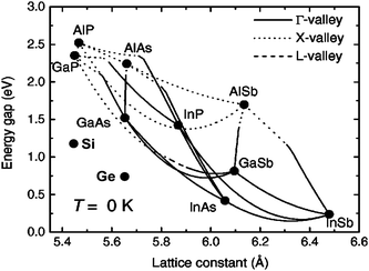 | ||
| Fig. 4 Band gap and lattice constant for various III–V and group-IV material alloys. | ||
For a device that is monolithic and series-connected, it also places some additional electrical requirements on the stack. The foremost is the current balance between subcells. As the device junctions are connected in series, the voltages of the diodes add up and the current is clamped by the subcell that produces the lowest current in the string. Note that since the tunnel junctions are assembled in reverse polarity they subtract whatever amount of voltage drop there is across them from the total device voltage. This can be expressed as VT = Vtc–Vtj1 + Vmc–Vtj2 + Vbc, therefore, it is imperative that tunnel junction voltage drops are minimized. In essence, the advantage for a monolithic multijunction with subcells connected in series is the gain in voltage but the trade off is a cell that produces lower current.
A key question to ask is which combination of band gaps should be chosen, and how much current will be produced in each device? The current density of the subcell scales with the band gap so lower current densities result from wider band gap materials. A hypothetical 3-junction device that uses an AM1.5G or an AM1.5D spectrum may then be used to theoretically calculate the available current and the proper balancing. In the ideal 3-junction device on Ge, this becomes ∼ 1.7 eV, 1.1 eV, 0.67 eV for the top, middle and Ge junctions, respectively. The GaInP/GaAs/Ge system is limited to 1.9 to 1.8 eV/1.4 eV/0.67 eV which are much higher in band gap than the ideal. The net effect is that the current produced within the Ge subcell is typically in excess by a factor of two than the upper junctions. Since it is the lowest band gap in the stack, the power from higher energy light that could be captured by a more optimal middle junction is lost and turned to heat. Many development efforts today are centered on the improvement of this balance to reach a more favorable device.
Current balancing between subcells is also important for multijunction CPV systems in the field. The spectral content of sunlight changes with varying weather and solar conditions as well as system optical design. For example, concentrator systems using lenses or mirrors do not transmit or reflect light perfectly at every wavelength. Therefore, care must be exercised in designing optimum cells and system components for the average system configuration.
Tunnel junctions are an additional consideration in designing a concentrator multijunction solar cell. In some applications the intensity of sunlight can reach as high as 100 W cm−2 which produces a current density of 14 A cm−2 in a modern 3-junction device for impinging rays at normal incidence. This imposes a design criterion on the tunnel junction in that the peak tunneling current must well be in excess of this limit. Additionally, the tunnel junction must have high transparency when light is passing through the device from the upper to lower junction. In the case of the upper tunnel junction shown above, the ideal case would be a tunnel junction formed of materials with a band gap exceeding the upper subcell such that it is completely transparent to light passing through. A caveat is that wider band gap materials can not be doped sufficiently high, so the general rule is that the upper limit of the effective doping drops with increasing band gap. The peak tunneling current is a direct function of the doping.45 There exists a trade space that must be optimized between peak tunneling current, transparency, and other engineering parameters such as cost, reliability, and manufacturability. This problem is one of the most difficult engineering challenges in the epitaxial stack of modern multijunction devices. Attaining efficiencies greater than 40% and large scale manufacturing of concentrator solar cells are a testament to the level of development achieved in present-day devices.
2.2 Next generation PV cell structures
In 3-junction GaInP/GaInAs/Ge metamorphic (MM) solar cells, the GaInP and GaInAs subcells can be grown on a metamorphic buffer such that these two subcells are lattice-matched (LM) to each other, but are both lattice-mismatched to the Ge growth substrate and subcell.30,46,47 Schematic diagrams of this upright, MM, 3-junction cell configuration, as well as the more standard LM 3-junction cell, are shown in Fig. 5. The mismatched design of the MM cell allows the upper two junctions to be grown with lower band gaps than in the LM case, which results in a more advantageous band gap combination for converting the solar spectrum.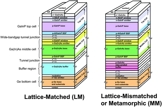 | ||
| Fig. 5 Cross-sections of lattice-matched (LM) and metamorphic (MM) GaInP/GaInAs/Ge 3-junction cell structures.27 | ||
The MM cell design uses a step-graded metamorphic buffer to transition from the lattice constant of the substrate to that of the upper subcells, as shown in Fig. 5. This buffer can be engineered to be nearly 100% relaxed, with very little residual strain to drive the formation of dislocations in the active upper subcells. The lattice mismatch in MM cells produces dislocations in the crystal structure, which lower minority-carrier lifetime and cell efficiency, but with suitable buffer design the density of these dislocations in the active regions of the subcells can be minimized. The shift in the quantum efficiency of the upper two subcells in GaInP/GaInAs/Ge 3-junction cells, as a result of the higher indium composition and lower band gap of the metamorphic GaInP and GaInAs subcells, enables these MM subcells to capture some of the current density that would otherwise be wasted in the Ge subcell.
In another type of metamorphic 3-junction cell design, the bottom subcell is replaced with a metamorphic ∼1 eV GaInAs subcell, grown in an inverted configuration.28,48–50 In this type of inverted metamorphic (IMM) cell, shown in Fig. 6, it is easier to grow the upper ∼1.9 eV GaInP and ∼1.4 eV Ga(In)As subcells with the desired band gaps at the smaller lattice constant of the substrate. So these subcells are grown lattice-matched to the substrate, either upright as in Fig. 6(a), or inverted as in Fig. 6(b). In both cases, the metamorphic ∼1 eV GaInAs subcell 3 is grown inverted on a transparent metamorphic graded buffer region that transmits light used by the ∼1 eV cell. For the configuration in Fig. 6(b) in which all 3 subcells are grown inverted, the original growth substrate is removed during cell processing to let light into the front surface of the inverted cells. The higher band gap of the bottom subcell in these IMM designs results in a higher voltage compared to LM 3-junction cells.
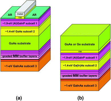 | ||
| Fig. 6 Two configurations of 3-junction solar cells with a highly-lattice-mismatched, inverted ∼1 eV GaInAs bottom subcell: (a) growth on two sides of a transparent GaAs substrate; (b) growth on the back of a GaAs or Ge substrate that is removed during cell fabrication.28 | ||
A 4-junction (Al)GaInP/AlGa(In)As/Ga(In)As/Ge terrestrial concentrator solar cell is shown in Fig. 7,29,51–53 indicating optional elements in the subcell composition in the parentheses. This type of cell permits dividing the photon flux available in the terrestrial solar spectrum above the band gap of the GaInAs subcell 3 into 3 pieces, rather than 2 pieces in the case of a 3-junction cell. As a result, the current density of a 4-junction cell is roughly 2/3 that of a corresponding 3-junction cell, and the I2R resistive power loss is approximately (2/3)2 = 4/9, or less than half that of a 3-junction cell. Fig. 7 shows a LM 4-junction cell, with all the subcells at the lattice constant of the Ge substrate, but MM versions of the 4-junction cell are also possible, giving greater flexibility in band gap selection. For example, the maximum theoretical limit on the efficiency for a 4-junction terrestrial concentrator device is just over 58%, with possibly realistic cell efficiencies of 47% for a material combination consisting of GaInP/AlGaInAs/GaInAs/Ge and associated band gap energies of 1.90/1.43/1.04/0.67 eV.53 This configuration also uses optically transparent metamorphic graded buffers which are key for joining layers in the MM approach. A design that incorporates a 4-junction IMM configuration comprising GaInP/GaAs/GaInAs(1 eV)/GaInAs(0.75 eV) has been proposed.54
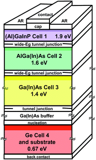 | ||
| Fig. 7 4-junction AlGaInP/AlGaInAs/GaInAs/Ge terrestrial concentrator solar cell cross section.29 | ||
Designs that push the concept of a multijunction solar cell bring new meaning to this technology when making the 5-junction and 6-junction devices proposed for space and terrestrial applications.51–53 A 5-junction configuration based on AlGaInP/GaInP/AlGaInAs/GaInAs/Ge has been studied before with projected efficiency of 42% and experimental 1 sun efficiency measuring 24.1%.55 An advanced 5-junction configuration consisting of AlGaInP/AlGaInAs/GaInAs/GaInNAs/Ge has been predicted to be capable of 55%.55 Historically, good quality GaInNAs is challenging to make and suffers from low minority carrier diffusion lengths which therefore hampers the carrier collection necessary for generating meaningfully high currents when GaInNAs is incorporated in a 4-junction stack.56 Six-junction cells were first grown and tested in 2004 with the following material structure: GaInP/GaInP/AlGaInAs/GaInAs/GaInNAs/Ge.27 Experimental 6-junction cells with this structure, incorporating a ∼1 eV dilute nitride GaInNAs subcell 5, were measured with an active-area efficiency of 23.6% under the AM0 spectrum.28 The potential efficiency of this structure has been calculated to be 58%.55 Using Eg/q - (kT/q)ln[AkTNCNVµn/(NALnIL)] as a close approximation to the open circuit voltage where Eg/q is the band gap voltage, A is the cell area, and referencing Fig. 4, this structure is capable of producing 5.25 V at 1 sun and perhaps well over 6 V at 500 suns. High voltage devices are advantageous in some CPV systems depending on the design requirements, but allow for stringing fewer solar cells in a series circuit.
A description of 3-, 4-, 5- and 6-junction solar cells to achieve higher efficiency has been carried out using techniques that consist of growing multijunction structures in an upright or inverted fashion. However, mechanically stacking specific cell structures is another way to merge junctions to form a multijunction device. Improvements in wafer bonding techniques have moved this technology to a point where joining semiconductor structures are performed with better quality and consistency, compared to the original methods that were pioneered in the past for bonding III–V PV cells such as GaAs/GaSb and GaInP on GaAs/GaSb.57–60 Although molecular bonding techniques and semiconductor wafer adhesive bonding using thermosetting and thermoplastic polymers have become more advanced, costs and lengthy processing is still an issue. Removal of the “sacrificial” substrate and achieving a uniform bond throughout a large epitaxial surface is time-consuming and challenging. Bonding 2-junction GaInP/GaAs/Ge to 2-junction GaInAsP/GaInAs/InP has been suggested before.61,62
Another approach consists of integrated optical systems in a PV design based on lenses, dichroic prisms, and/or multijunction component cells where the solar spectrum is split into multiple bands with each corresponding to the spectral response of each component cell.63,64 For example, the solar spectrum can be divided three ways, to illuminate GaInP/GaAs, GaInAsP/GaInAs and Si solar cells.65 These component cells were built, and each was measured separately by NREL, using the spectrum predicted to be incident on the cells in a spectral splitting system, assuming 100% optical efficiency. If the electrical power outputs from each of the cells at their various currents and voltages could be combined with 0% electrical losses to form a single power output, these efficiencies would sum to 42.8% efficiency. This is an important demonstration of the concept and use of spectral splitting PV configurations. Future investigations will include work on these system integration issues, to achieve an optical and electrical efficiency associated with combining the cells approaching 100%, and to address the device mounting costs for multiple discrete solar cell components.
Multijunction solar cells using the MM structure like the one shown in Fig. 5 are the first photovoltaic cells of any kind to cross over the 40% efficiency barrier. Such high efficiency cells come at the expense of establishing low resistive metal contacts. Proper metal contacting schemes are important in achieving low contact resistance at high solar flux to help in maximizing cell performance. This is discussed in the next section.
3 Metal semiconductor contacts
In the previous section, important material properties were discussed to design the structure of multijunction solar cells for optimum operation under a terrestrial spectrum. Different device architectures with the potential to maximize usage of the solar spectrum were shown. To effectively draw the current from the device, the formation of a low resistive interface at the metal–semiconductor junction is necessary. In this section, the principles behind the operation of metal–semiconductor contacts will be briefly examined along with techniques to minimize the resistance at the interface, or contact resistivity. A detailed description of the physics of metal–semiconductor junctions can be found elsewhere.66Depicted in Table 1 are the work functions, qϕm, of common metal contacts and their measured Schottky barrier heights for some technologically important semiconductors. It is important to note that for high current devices as in the case of concentrator cells, quasi-ohmic contacts are imperative for high performance device operation. This means that for a highly doped semiconductor, the Schottky depletion region becomes quite narrow and therefore, the width of the barrier becomes thin enough to allow electrons to be injected in the metal through thermionic-field emission. This process takes place by quantum mechanical tunneling as shown in Fig. 8.
| Metal contact | Work function (qϕm; eV) | n-Type semiconductor | p-Type semiconductor | ||||
|---|---|---|---|---|---|---|---|
| Barrier height (qφBn; eV) | Barrier height (qφBp; eV) | ||||||
| GaAs | Ge | Si | GaAs | Ge | Si | ||
| a Ref. 67. b Ref. 68. c Ref. 69. d Ref. 70. e Ref. 71. f Ref. 72. | |||||||
| Ag | 4.26 | 0.88 | 0.54 | 0.78 | 0.63 | 0.50 | 0.54 |
| Au | 4.80 | 0.90 | 0.59 | 0.80 | 0.43 | 0.30 | 0.34 |
| Al | 4.25 | 0.80 | 0.48 | 0.72 | 0.61f | 0.58 | |
| Pt | 5.30 | 0.98a | 0.90 | 0.22 | |||
| Cr | 4.50 | 0.80b | 0.61 | 0.50 | |||
| Ni | 4.50 | 0.83c | 0.61 | 0.51 | |||
| Pd | 5.12 | 0.78 | 0.81 | 0.42 | |||
| Ti | 4.33 | 0.75d | |||||
| W | 4.60 | 0.90e | 0.48 | 0.67 | 0.45 | ||
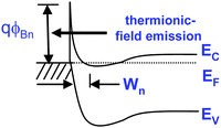 | ||
| Fig. 8 Energy band diagram of a narrow Schottky barrier formed with highly-doped n-type semiconductor. | ||
Since thermionic-field emission occurs below the top of the Schottky barrier and not over the barrier height, this implies that carrier injection is somewhat independent of the barrier height. Therefore, the higher the doping concentration in the semiconductor, the narrower the barrier width and higher the probability of the electron tunneling through the barrier regardless of the barrier height. Fig. 8 suggests that a low resistive contact can be obtained from the Schottky interface with semiconductor heavily-doped because of the low junction resistance that is encountered by the electrons. It takes less energy to tunnel through the junction than to surmount the junction barrier. Such a contact is defined as an ohmic contact, and is required for multijunction concentrator solar cells. Current flows through the device with little parasitic voltage losses and obeys Ohm's law where these losses scale with the amount of current flow; that is, the current–voltage characteristic is linear. Ideally, low work function and high dopant concentrations in a n-type semiconductor are desired for low resistance ohmic contacts. Preferably, the metal work function should be less than or equal to the work function of the semiconductor, however, such a contact is practically nonexistent. For p-type material, the metal work function should be equal to or greater than that of the semiconductor to form a good ohmic contact. High doping in the semiconductor is also favorable to obtain good ohmic behavior. The issue is that there are not high enough work function metals that are suitable for making good contacts to a p-type semiconductor.
So far, metal–semiconductor interfaces have been discussed without including surface states. In reality, surface states are predominant in all semiconductors due to the periodicity of the crystal lattice terminating at the surface with dangling bonds. To illustrate their magnitude, consider the following simple calculation for GaAs with lattice constant of 5.65 Å. The unit cell surface area is 5.65 Å × 5.65 Å yielding 3.1 × 10¹⁴ unit cells cm−2. Since there are 4 dangling bonds in each unit cell, the total number of surface states is 1.2 × 10¹⁵ unit cells cm−2. This amount is significantly high, and their effects on the barrier height can not simply be ignored but discussing this in detail is outside the scope of the review. Worth mentioning, however, is that typically dangling bonds deplete the surface charge of the semiconductor causing band bending even in the absence of a metal contact, which makes it cumbersome to form extremely low resistive ohmic contacts. Here Fermi level pinning occurs at these surface states within a narrow energy distribution in the band gap. In GaAs, for example, Fermi level pinning to surface states fixes the barrier height between 0.7 to 0.9 eV below the conduction band at the interface regardless of the value of the metal work function. There are methods to lessen pinning at the surface but typically these entail elaborate cleaning recipes with in situ cleaning in vacuum followed by metal deposition, requiring costly specialized equipment.
Many metal stack schemes exist today for forming low resistance contacts. Some have practical applications for manufacturing commercial devices, and others are more suited to the research laboratory. Frequently, stacks consisting of multilayer metals are used but a stack with a single metal is seldom employed. Most multijunction solar cells use GaAs as a capping layer since this material is lattice matched to many of the technologically important III–V binary and ternary compounds. The key to achieving good quasi-ohmic behavior is to dope the semiconductor substantially high. Contacts containing Ti on n+–GaAs have important benefits. Titanium is highly reactive with oxygen, and depositing it in a high vacuum evaporator chamber is always required. An initial flash of Ti on GaAs is necessary in promoting the adhesion for the subsequent base metal layers that constitute the bulk of the contact to conduct current, or can be used to join non-alloying metals as in the case of PtTiGePd/n+–GaAs73 and AuPtTiGePd/n+–GaAs.74 Contacts using the latter metallization stack were employed in AlGaAs/GaAs multijunction solar cells. The solid state reaction between Pd and GaAs creates As vacancies that Ge atoms occupy giving rise to a low resistive alloyed contact. Titanium also plays a role as a diffusion barrier to prevent Pt from reacting with GaAs since PtAs2 forms a stable intermetallic compound which is known to introduce reliability issues when annealed above 400 °C.
Other methods for making low resistive ohmic contacts involve using heterojunction techniques. One method includes depositing thin epitaxial n+–Ge on n+–GaAs since the lattice constant of Ge and GaAs are closely matched to within 0.5%.75 Another method employs forming a low band gap material such as InAs on a graded GaInAs buffer layer which in turn is deposited on GaAs. Since InAs directly in contact with GaAs forms an abrupt junction at the interface due to the conduction band discontinuities between the two materials, a graded GaInAs layer is necessary to “smooth” their band offset.75
Gold–germanium front contacts and Ti/Ni/Au back contacts have been used on multijunction GaInP/GaAs concentrator solar cells grown on GaAs substrates for operation at 1000 suns.76 A metallization that consists of Au/BeAu/Cr/p+–GaAs for the front contact, and AuNiAuGe/n+–GaAs on the back have been used on GaAs concentrator solar cells with low specific contact resistivies.77
As mentioned above, the specific contact resistivity, ρc (in Ω cm2) is an important parameter that is given considerable attention during multijunction device fabrication. For example, a 1 × 1 cm2 concentrator solar cell with ρc = 10−3 Ω cm2 operating at 50 W cm−2 of incident sunlight that is 35% efficient can boost the efficiency to 37% for ρc of 10−5 Ω cm2. Contact design depends on many factors such as contact metal, semiconductor material, dopant concentration, deposition technology, contact fabrication process; all of which influence ρc with values ranging from 10−3 to 10−7 Ω cm2.
For example, a study of ρc as a function of heat-treating four front metal contact schemes was carried out, namely: Pd/Ge/Ti/Pt/Ti/Ag/Au, Ti/Pd/Ag/Au, Ti/Pt/Ag/Au, and Ti/Ag/Au; all of which were deposited on heavily-doped n+-type GaAs. Also, a comparison of ρc between rapid thermal processing (RTP) and sintering in a furnace tube was performed. In RTP, heat-treating specific regions of a semiconductor device can take place in a fast and controlled environment but lack the capability of annealing a large number of wafers or devices. Furnace sintering is ideal for heat-treating wafers with large throughput but is time-consuming and can degrade the device structure as result of its inherently long thermal budget to process the device contact. Both techniques were used to examine contacts formed on etched GaAs mesa structures necessary to eliminate spurious current paths and to maintain unidirectional current flow. Only the Pd/Ge/Ti/Pt/Ti/Ag/Au and the Ti/Au/Ag contacts both received RTP and furnace sintering. The contact resistance (in Ω) was measured with the four-point probe technique, and ρc was then calculated from the size of the metal pads. The results from the study are depicted in Fig. 9.
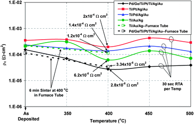 | ||
| Fig. 9 Specific contact resistivity evaluation from different contact schemes for the top metal grid structure subject to RTP and sinter. The solid lines represent samples that were annealed in RTP. The dashed lines are for those that were sintered in a furnace tube. The accuracy of the data is ±5 × 10⁻⁵ Ω cm2. | ||
Since the n-type GaAs cap is heavily-doped (>1018 cm−3), ρc is relatively low for the as-deposited metal contacts producing a moderately good non-alloyed ohmic contact as evaluated from dark current–voltage measurements. Typically, however, metal adhesion is poor for non-alloyed contacts and annealing is required. After the first heat treatment at 350 °C, insufficient heat is available to form a solid state reaction between the metal and the semiconductor as a result of not breaking Pt–Pt bonds and the Au–Au bonds (about 2/3 of the Pt–Pt bond energy) which are relatively high in the Ti/Pt- and the Ti/Au-based contacts. For the Pd-based contacts, alloying is beginning to occur due to the lower Pd–Pd bond strength (about 1/4 of the Pt–Pt bond energy) which is also evident from the decrease in ρc. Specific contact resistivity reaches a minimum at 400 °C for both RTP and sintering but RTP produces the lowest values. Note that Ti/Au/Ag reaches a lower ρc than Ti/Pt/Ag/Au since the former is more reactive at 400 °C than the latter because of the lower reactivity (higher energy needed to break Pt–Pt bonds) of Pt than Au. Many applications have used contacts containing Pt serving as a diffusion barrier to prevent the base metal from diffusing in the semiconductor at elevated temperatures. Higher temperature anneal (450 and 500 °C) produces an oscillating effect in ρc possibly due to the increased outdiffusion of Ga and As, and formation of electrically inactive phase domains and significant interdiffusion between Ti and Pt, Ti and Au and Ti and Pd which degrade their intended function and therefore, deteriorating ohmic behavior. Among the input parameters for modeling the front grid metallization spacing of multijunction solar cells is ρc which is discussed in the next section.
4 Device modeling
In the CPV industry, a 1 × 1 cm2 triple-junction solar cell is an appropriate size to illuminate with an optical concentration of 500 suns although smaller cell sizes are also being considered for the same concentration and higher concentration applications. At 500 suns, the short-circuit current is 7 A. Such high current densities create challenges in terms of ohmic power losses and heat dissipation. In order to maintain high cell efficiency, power loss mechanisms must be minimized. Device modeling is used to identify the limiting loss mechanisms and drive changes in the cell design to boost efficiency.Finite element analysis may be used in determining tie-detailed electric field profiles and current flow within the many layers of a multijunction cell. However, first-order insight into multijunction performance can be gained by considering the current flow shown in Fig. 10. Power loss due to series resistance occurs in three segments: (1) Resistance in the semiconductor layers, (2) contact resistance at the semiconductor–metal interface, and (3) resistance in the metal gridlines. In some cases, tunnel junction resistance may be included in the modeling for cells operating at higher concentration as this can impact the device performance above 1000 suns, specifically, for wider band gap tunnel junctions.
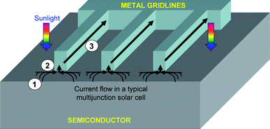 | ||
| Fig. 10 Current flow in a multijunction cell. Current is collected by the gridlines and then it flows to the busbar. | ||
Each of the three resistive loss mechanisms may be reduced by appropriate changes in the cell architecture. To reduce resistance in the semiconductor, for example, the emitter and window layer thicknesses (refer to Fig. 3 in section 2.1 above for a description) as well as doping may be increased. Such increases will eventually begin to degrade the performance of the p–n junctions, at which point an optimum thickness should be sought. Similarly, to reduce contact resistance and series resistance the metal gridline width can be increased up to an optimum point, before obscuration by the gridlines begins to limit cell performance. To reduce the obscuration, metallizations providing low contact resistance (as discussed in section 3) and high aspect ratio are employed, to the extent allowed by cost considerations. At the high current densities obtained in high CPV, the area covered by metal gridlines is still almost 10% of the semiconductor surface. In order to obtain the optimum gridline pitch the three resistive loss components may be combined with obscuration and modeled as a function of gridline spacing.
As shown in Fig. 11, the minimum power loss determines the correct gridline spacing as shown by the red line plot for a GaInP/GaInAs/Ge solar cell that operates at 500 suns. Certain loss mechanisms have greater influence on the lowest fractional power loss than others as shown in the figure for ρc and ρs. For example, two orders of magnitude change in ρc gives a change in minimum power loss from 28 to 21.7% while only a factor of 5 drop in ρs represents a change in minimum power loss from 23.7 to 21.7%. Clearly, at 500 suns small changes in ρs produce the largest changes in the fractional power loss.
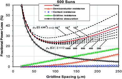 | ||
Fig. 11 Modeled combined loss mechanisms for a CPV multijunction cell with aperture area of 2.25 cm2, and a single busbar. The input parameters for the solid line are: ρc = 10−5 Ω cm2 and ρs = 1000 Ω/![[rectangle open, vertical]](https://www.rsc.org/images/entities/char_25af.gif) . The dependence of ρc (shown above the solid red line) at 1000 Ω/ and ρs (shown below the solid red line) at 10−5 Ω cm2 on the fractional power loss curve are shown. The solid lines with open symbols are the losses considered in the model. . The dependence of ρc (shown above the solid red line) at 1000 Ω/ and ρs (shown below the solid red line) at 10−5 Ω cm2 on the fractional power loss curve are shown. The solid lines with open symbols are the losses considered in the model. | ||
It should be noted that the model shown in Fig. 11 is only specific to the conditions dictated by the design boundary conditions such as multijunction material composition and properties, ρc, ρs, solar flux, flux uniformity, grid configuration, gridline width and height. Each solar cell will require a specific set of conditions to design a device that is optimized to operate at the intended solar flux.
5 Principle of operation under concentrated sunlight
So far the discussion has been devoted to designing high efficiency multijunction solar cells for use at high solar flux. Understanding how these cells function under a given spectrum is crucial in tailoring the device structure for operation in different environments, whether the device is freely collecting sunlight or is absorbing filtered light in the presence of a lens; or even if the device is operating near dawn or dusk. In any case, using the proper spectrum is helpful for device design. One of the standard reference spectra for this purpose is the ASTM G173-03 spectrum as illustrated in Fig. 12. This spectrum is similar to the low aerosol optical depth (AOD = 0.085) AM1.5D spectrum which has been used as the standard reporting spectrum by NREL for multijunction CPV.29 One key difference for this spectrum is the reduction in the off-axis blue component compared to the global spectrum; the latter boasting all wavelengths advantageous to the flat plate industry.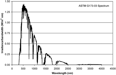 | ||
| Fig. 12 The ASTM G173-03 terrestrial solar spectrum relevant for multijunction CPV. | ||
5.1 Sensitivity to specific spectral bands
With reference to Fig.12, each subcell in the GaInP/GaInAs/Ge multijunction stack responds to a specific spectral band with the combined subcells making more use of the sun's spectrum than single-band absorption from conventional cells. Considering the ASTM G173-03 standard spectrum with intensity of 0.0901 W cm−2, the multijunction device with band gaps of 1.84 eV/1.42 eV/0.67 eV captures 0.0862 W cm−2 of sunlight, discarding only 4% of unusable light. Variations in intensity of the spectrum, whether due to atmospheric conditions, use of absorptive or reflective optics in a CPV system or some shadowing effect will affect the current output from each subcell.The ability of a solar cell to absorb light at each wavelength within a specific spectral band and therefore, generating electric current is termed spectral response (in units of A/W). The quantum efficiency (QE) is a measure of how many photons in the spectral band are absorbed by the minority charged carriers and subsequently collected by the device to form useful current. Measuring the QE from each subcell in the multijunction device provides invaluable information about epitaxial layer characteristics, and can give details about the total current in each subcell along with their individual current components; all retrievable from modeling. Describing the current transport equations for this modeling is outside the scope of the present discussion but their derivation and use can be found in the literature.78 To gain some understanding on what semiconductor layer parameters affect the spectral response, consider the QE plots shown in Fig. 13.
Typically, the blue response of the solar cell is sensitive to certain emitter layer characteristics as shown in Fig. 13 for a modeled external QE curve of GaInP used in the top cell of multijunction devices. Four QE components contribute to the overall QE for this subcell; the base layer, the emitter layer, the depletion layer and the window layer. (Refer to Fig. 3 for the location of these layers.) Note that the emitter QE has a peak at the point where maximum blue absorption has occurred in the top subcell, which is nearly at 380 nm. This is due to the high absorption coefficient of GaInP which is in the high 105 cm−1 range near this wavelength. Two points worthy of note are that (1) thicker emitter layers give rise to poor blue response as shown in the figure for plots (b) to (d), usually as a consequence of the formation of a “dead layer;” (2) and a low dopant concentration will also contribute to degradation of blue light absorption as well. If these points are present simultaneously, then they will have detrimental effects on the subcell QE. The same can be inferred for the window layer although the effect is moderate. However, for the model used in Fig. 13, the window layer thickness was held constant. For the peak QE in the base, however, after light passes through the window, emitter and depletion layers; the available lower energy photons become absorbed and contribute to the QE in this region. In summary, changes in the emitter thickness, emitter dopant concentration, depletion width, hole minority carrier diffusion length in the emitter and window, and the window thickness influence the QE curve between 350 and 550 nm. While changes in the base thickness, dopant concentration, electron minority carrier diffusion length; and to a lesser extent, the depletion width and emitter layer thickness affect the QE curve between 500 and 675 nm.
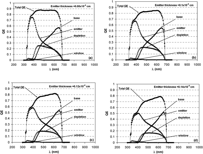 | ||
| Fig. 13 Modeled external quantum efficiency of a GaInP top cell showing the contributions from each semiconductor layer. For the emitter; Sp = 5 × 103 cm s−1, tE = variable as illustrated in plots (a) to (d), and Dp = 10 cm2 s−1. For the base; Sn = 1 × 105 cm s−1, tB = 10−4 cm, Dn = 150 cm2 s−1, and the depletion layer width, W, is 0.08 µm. | ||
5.2 Voltage increase with concentration
Fig. 14 displays a typical current-bias characteristic for a solar cell under illumination. There are two current mechanisms that flow in opposite direction for a solar cell in this condition: the photogenerated current that can produce power, and internally generated dark current that can be thought of as a dissipative current that degrades efficiency. The open circuit voltage, Voc, in Fig. 14 denotes the point in the illuminated current–voltage characteristic where the internally generated dark current equals the illumination current. At biases below Voc, the solar cell produces power that can be transferred to a resistive load and utilized. At biases above Voc, the dark current exceeds the illumination current and no useful power can be extracted from the cell. The maximum power point, Pmax, is defined as that point where the I–V product is maximized and many power-supplied systems are designed to operate at or very close to this point. In typical high quality solar cells the maximum power point is engineered to be very close to Voc. Thus high Voc is desirable and several approaches are available to accomplish this.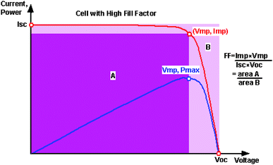 | ||
| Fig. 14 The forward bias current versus bias characteristic for a solar cell. The short circuit current (Isc) and open circuit voltage (Voc) both increase with illumination concentration. | ||
Reducing the operating temperature of the solar cell will increase Voc because at lower temperatures the internally generated dark current is reduced; typically the dark current scales exponentially with temperature. In many instances, however, this approach proves to be impractical as solar cell power-generating systems are designed simply for minimizing the temperature rise of the cells in operation so not to significantly degrade Voc.
Increasing the photon flux density through concentration techniques using refractive or reflective optics is another approach to increasing Voc, and it is this approach that finds widespread application in CPV systems. The mathematical explanation for this phenomenon is detailed in eqn (1) on the basis of a lumped equivalent circuit model, and application of Kirchoff's rules;
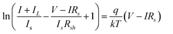 | (1) |
A key benefit of multijunction solar cells is the subcell voltages are additive according to Kirkoff's voltage law as illustrated in Fig. 15. For 1 sun and 10 suns, each voltage from the GaInP, GaInAs and Ge junctions add giving the overall voltage of the 3-junction cell. In essence, 1.22 V + 1.04 V + 0.25 V = 2.51 V for the 1 sun case, and 2.72 V for 10 suns. As mentioned above, Voc increases with increasing concentration for each subcell as is evident from 1 to 10 suns in the figure, corresponding to a total voltage increase of 0.22 V for the 3-junction device. This can be understood as follows. Photons hit the cell creating electron–hole pairs; electrons from the p side flow across the junction to the n side becoming majority carriers and holes from the n side flow to the p side becoming majority carriers as well due to the built-in electrical field at the junction. This redistribution of carriers sets up a potential difference, or Voc which results from the splitting of the thermal equilibrium Fermi level (EF) into the minority carrier electron quasi-Fermi level, EFn, and the minority carrier hole quasi-Fermi level, EFp. Their difference gives Voc ≈ (EFn - EFp)/q When more photons are impinging on the cell, the separation of the quasi-Fermi levels increases further and Voc increases. This will be the case for the Voc in each subcell junction with their combined increase augmenting the Voc of the multijunction device with higher photon flux. Another mechanism of why concentration improves Voc, and consequently cell efficiency, could be interpreted by a simple area argument. Internal dark current scales with solar cell area. A factor of say 10x reduction in solar cell area can be used when concentrating the solar illumination ten times without any loss in the total number of photons absorbed and converted to useful power. The same output power is realized but the efficiency-robbing dark current has been reduced by a factor of 10. Note that this argument cannot be carried to the limit of infinite concentration or zero solar cell area. The 2nd law of thermodynamics limits Voc and the conversion efficiency through terms in the dark current that are not negligible as concentration increases or the cell area goes to zero.79 In addition, practical solar cells do not have perfect series and shunt resistance characteristics and these also limit the voltage at maximum power and fill factor.
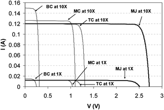 | ||
| Fig. 15 The modeled IV characteristics of a typical triple junction GaInP/GaInAs/Ge solar cell under 1x and 10x concentrations. Voc increases are observed for the top (TC), middle (MC) and bottom (BC) subcells, as well as the multijunction cell. Each subcell Voc was increased as follows: TC; 1.22 to 1.31 V, MC; 1.04 to 1.10 V, BC; 0.25 to 0.31 V, MJ; 2.51 to 2.72. All IV curves have Rs = 0. | ||
5.3 Fill factor increase with concentration
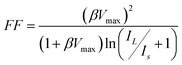
Fig. 14 above illustrates the concept of fill factor, FF. For any given level of concentrated sunlight, the real current-bias characteristic will never be a rectangle, with the maximum power equal to Imp × Vmp, due to an assortment of loss mechanisms in the device such as (1) resistance through the gridlines, (2) semiconductor resistance in the top cell, (3) tunnel junction resistance, (4) shunt resistance, (5) contact resistance, and (6) resistance due to externally making electrical contact to the solar cell. As the concentration increases, the maximum power point moves slowly toward Voc and FF gradually approaches unity. The mathematics behind this can be understood through manipulation of eqn (1). Assuming a lossless cell with Rs = 0 and Rsh = ∞, an expression in terms of the maximum voltage, Vmax, for which power can be drawn from the device is given by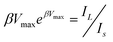 | (2) |
 | (3) |
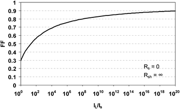 | ||
| Fig. 16 The fill factor versus current scaling factor to 20 orders of magnitude for an ideal solar cell. | ||
In all PV cells, the FF is an important parameter that gives information about the quality of the solar cell, and often serves as a tool to diagnose whether a multijunction solar cell is operating in a current matched or mismatched mode. For example, depicted in Fig. 17 is a case when the subcell currents are mismatched (a) and (b), and when their currents are matched (c) in a 3-junction cell. For the instance where the subcell current configuration in Fig. 17(a) transitions to Fig. 17(b) is when highly absorptive optics attenuates a substantial portion of the infrared component of the solar spectrum under concentrating sunlight, or when the solar cell is purposely designed to operate in this way. Another case can develop as shown in Fig. 17(c). Such a situation can happen when using a poly(methyl methacrylate) (PMMA) lens or window with strong absorption bands near 1300 and 1600 nm.80 These absorption bands can starve the Ge bottom cell from the light it needs to generate excess current. Here the FF of the 3-junction cell is a combination of the fill factors from each subcell, thus providing sort of an average integration of the “knee” from the subcell IV curves. Table 2 shows the values for all three cases. When designing a solar cell, consideration must be given to the amount of current that should be available in the Ge subcell so that it does not limit the overall current in the multijunction cell when in the presence of high absorbing optics. Another example that reveals the usefulness of the FF as a diagnostic, deals with monitoring the current mismatch between the top and bottom cells in a 2-junction tandem solar cell as a result of spectral variations from the optics in a CPV module.81 Putting optical effects aside, series resistance always has a dominant effect on the FF.
| All Isc's mismatched | MC & BCIsc's matched | All Isc's matched |
|---|---|---|
| 87.9 | 87.9 | 87.9 |
| 86.1 | 86.1 | 86.3 |
| 70 | 71 | 71 |
| 88.6 | 86 | 84.8 |
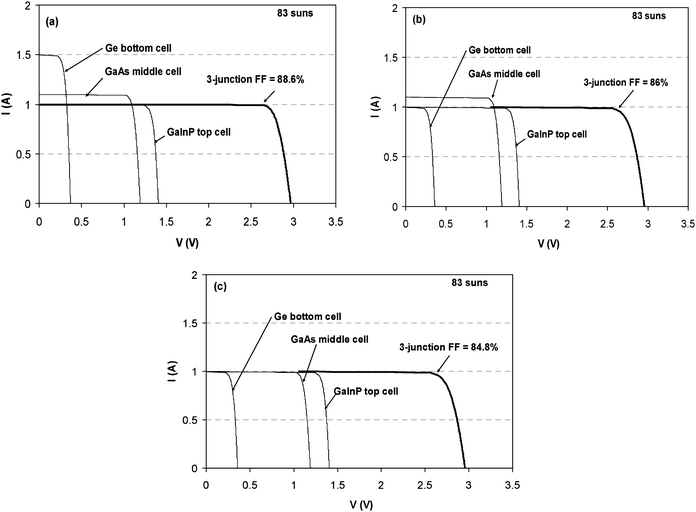 | ||
| Fig. 17 The effects of current mismatching and balancing the top, middle and bottom subcells on the 3-junction cell fill factor. (a) A situation when the fill factor is 88.6% for mismatched subcell currents. (b) When the middle and bottom subcells currents are matched the fill factor is 86%, and (c) when all subcell currents are matched the fill factor is 84.4%. | ||
5.4 Series resistance
Imperfections in multijunction solar cells due to non-zero series resistance as well as shunt resistance less than normal will degrade the current bias characteristic and introduce a shape that deviates from a perfect rectangle at all light concentration levels. In particular, a finite series resistance will eventually limit the increase in FF with concentration, and a maximum point will be reached for any practical solar cell. As illustrated in Fig. 18, an increase in series resistance clearly degrades FF at both 83 suns and 500 suns concentration factors. Upon introduction of 0.1 Ω of series resistance, the FF is reduced from the ideal case of 90% to 87% at 83 suns, and from 90% to 71% at 500 suns. High quality solar cells have series resistance less than 0.1 Ω so that operation at 500 suns or higher can take place with negligible losses. However, higher than this concentration can lead to voltage drops due to parasitic losses which will limit conversion efficiency. In section 6, Fig. 20 shows the FF for several types of high quality 3-junction solar cells with maxima between 100–500 suns.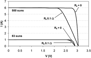 | ||
| Fig. 18 The introduction of series resistance at 83x and 500x concentration for a 3-junction GaInP/GaInAs/Ge solar cell significantly reduces the quality of the solar cell current-bias characteristic and hence FF. The IV curves were modeled using the ASTM G173-03 spectrum. | ||
Series resistance occurs in all solar cells from the simplest device architecture to the most complex 4-, 5- and 6-junction solar cells. The predicted gain in power from the boost in voltage, however, is encouraging enough to study these devices of higher number junctions which should offset the losses encountered from series resistance.
All semiconductor solar cell p–n junctions obey eqn (1) where Voc has a linear logarithmically dependent behavior on the concentration level while Vmax is nonlinear, as shown in Fig. 19. It is important to note that for a high quality cell, series and shunt resistance (if this term is not too low) have no effect on the Voc since the current flow through the device is zero. In contrast, the Vmax is dependent on both the series and shunt resistance terms as is evident in Fig. 19 for two values of the lumped series resistance. In this case, current flows through all the resistive loss mechanisms in the device as mentioned in Fig. 11, which give rise to voltage drops that subtract from Vmax. Temperature also affects Voc and Vmax, and is mentioned next.
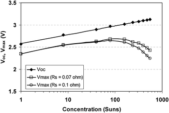 | ||
| Fig. 19 Calculated Voc and Vmax for a GaInP/GaInAs/Ge 3-junction solar cell. The Rsh = 1.5 × 10⁴ Ω. | ||
Under concentrated sunlight, about 37% of the energy absorbed in a GaInP/GaAs/Ge solar cell is used for generating electrical power whereas the other 63% is dissipated in heat. This means that for a cell with emissivity, ε = 0.85, the temperature at the surface of the solar cell with incident solar intensity of 50 W cm−2 could reach an equivalent blackbody temperature of 1300 °C in the absence of cooling; high enough to melt some metals. Heat dissipation is important because the Voc is a decreasing function of temperature, which is represented by temperature coefficient in terms of mV/°C. For example, the Voc temperature coefficient at 50 W cm−2 (555 suns based on the ASTM G173-03 spectrum) for multijunction GaInP/GaInAs/Ge is −4.3 mV/°C; as recently reported in a study examining the effects of temperature on solar cell performance.82 Any temperature changes in Voc are due to corresponding temperature changes in the band gap. Despite the negative effects of temperature on the Voc, the net voltage increase is typically between 450 and 550 mV at 50 W cm−2 compared to the 1 sun Voc during outdoor tests for a cell temperature of 25 °C. Next, efforts focusing on meeting manufacturing goals of increasing the cell efficiency in volume production deserve special note and are covered in the following section.
6 Key results
As already discussed, III–V multijunction cells have reached an important milestone for photovoltaics: a metamorphic GaInP/GaInAs/Ge 3-junction cell was the first to jump over the 40% milestone with 40.7% efficiency at 240 suns measured in 2006 (24.0 W cm−2, AM1.5D, low-AOD, 25 °C).30,31,53 A LM 3-junction cell has also achieved over 40% efficiency, with 40.1% (13.5 W cm−2, AM1.5D, low-AOD, 25 °C) measured at 135 suns.30,31,53Fig. 20 depicts the measured light IV curve for the 40.7% efficient cell. Recently, an inverted metamorphic structure has reached a new record efficiency of 40.8% under the standard concentrated terrestrial spectrum at 326 suns.32 The record efficiencies listed above have all been independently certified by NREL. Additionally, these record efficiency cells are monolithic, two-terminal cells, facilitating their implementation in production and in cost-effective concentrator systems.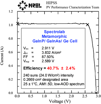 | ||
| Fig. 20 Illuminated I-V curve for the 40.7% metamorphic 3-junction cell designed and built at Spectrolab.30,31,53 | ||
In Fig. 21 are shown the best cell efficiencies from current multijunction technology developed at Spectrolab plotted as a function of concentration.30,31,53 Champion cell efficiencies of 40.1% and 40.7% have been obtained from the LM and MM structures, respectively. Roll-off in the FF between 100 and 1000 suns is due to the series resistance terms like those in Fig. 11 above. As described in ref. 30, the high efficiency of this MM cell approach comes about because the spectral distribution of photon energies from the sun favors the lower band gaps for the upper two subcells in the MM case, compared to the somewhat higher band gaps from the GaInP and GaAs system grown lattice-matched to a Ge substrate. Solar cells built from the MM approach are expected to provide the highest efficiency devices that could reach 45%, and potentially 50% efficiency in the next few years.30
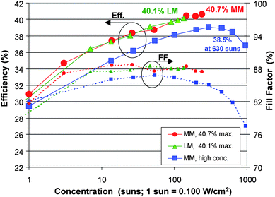 | ||
| Fig. 21 Plot of efficiency vs. concentration from ref. 31 and ref. 53 for various device architectures including the 40.7% efficient metamorphic cell, the first solar cell to reach over 40% efficiency.30 The performance from each cell has been certified at NREL. At higher concentrations, the efficiency begins to drop due in part to the roll off in the FF. | ||
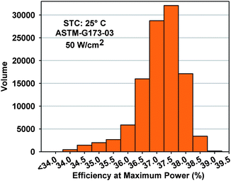
Transfer of some of these high performance cell technologies into production has been on-going, and has been successfully demonstrated by the efficiency distribution of 110![[thin space (1/6-em)]](https://www.rsc.org/images/entities/char_2009.gif) 000 C1MJ (Concentrator, 1st Generation Multi-junction) solar cells, as shown in Fig. 22. The C1MJ cells were introduced in 2007 as the first volume production phase of terrestrial, multijunction concentrator solar cells at Spectrolab. Under standard test conditions (25 °C, ASTM–G173-03 spectrum) and 50 W cm−2 of incident solar radiation, these cells show an average (mode) efficiency of 37.5%. These data were produced from 1 × 1 cm2cells with their structure designed from the 3-junction, lattice-matched, GaInP/GaInAs/Ge baseline. Despite the fact that this population does not represent the total throughput, 110000 solar cells represent a capacity of more than 2 MW of CPV at peak power. The 2nd generation product, C2MJ, is projected to have a mode efficiency of 38.5%, and is expected to be qualified in the third quarter of 2008.
000 C1MJ (Concentrator, 1st Generation Multi-junction) solar cells, as shown in Fig. 22. The C1MJ cells were introduced in 2007 as the first volume production phase of terrestrial, multijunction concentrator solar cells at Spectrolab. Under standard test conditions (25 °C, ASTM–G173-03 spectrum) and 50 W cm−2 of incident solar radiation, these cells show an average (mode) efficiency of 37.5%. These data were produced from 1 × 1 cm2cells with their structure designed from the 3-junction, lattice-matched, GaInP/GaInAs/Ge baseline. Despite the fact that this population does not represent the total throughput, 110000 solar cells represent a capacity of more than 2 MW of CPV at peak power. The 2nd generation product, C2MJ, is projected to have a mode efficiency of 38.5%, and is expected to be qualified in the third quarter of 2008.
 | ||
| Fig. 22 Efficiency distribution of 110000 C1MJ solar cells. | ||
An important aspect of making high efficiency concentrator solar cells is to ensure that they operate continuously in the field without any reliability issues. At first, it may be tempting to just adopt the protocol used for qualifying Si cells in the flat-plate industry, or even for Si concentrators but for multijunction devices, a whole set of different parameters that are inherent to this technology would preclude this from taking place. Qualifying multijunction cells must first look at correcting the short-term realibility problems from screening and environmental tests under operation in concentrated light, and then followed by the more ambitious goal of simulating long-term field operation to obtain sound reliability data.
7 Environmental testing and reliability
The long-term reliability field data of III–V multijunction cells in terrestrial concentrator systems is unknown, but there is good reason to believe they will perform well. This is because their device relatives have performed superbly in space for over a decade. Only short-term field data is available for installed systems by Solar System PTY which uses triple junction solar cells with the wider band gap GaInP top cell in their CS500 dish, Concentrix which employs the CX series FLATCON modules and Arizona Public Service (APS) with the Ctek point focus design.16–18,36 These companies have reported installed system field data as early as 2004 for APS, as an example. As a result of this background, much of the environmental, qualification and reliability tests can be focused on differences in the environmental conditions and packaging.Packaging and system design has significant impacts on cell reliability. Many reliability issues can be avoided by designing a good system. Some design considerations to improve reliability are listed below:
• Substrate assembly coefficient of thermal expansion matched to Ge
• Stress relief at interfaces
• Uniform and low thermal resistance to heat sink
• Isolation of mechanical stresses (interconnection, secondary optics, etc)
• Moisture protection for cell and connections
• Reduction of polymers in optical path
The best test, and the longest, is exposure to real operating conditions. It is recommended to put actual solar cells into the field, preferably in different environments (e.g. Phoenix and Florida), as soon as representative operating samples can be built. Table 3 shows some requirements and their measured (or expected) impact of severity on the device under study. Field trials should include adequate monitoring equipment to track cell performance with ambient conditions from year to year.
| Condition | Relative severity |
|---|---|
| Spectrum | Different & variable |
| Temperature | Different |
| Moisture | Higher |
| Thermal cycle | Lower |
| Vibration | Lower |
| Current density | Higher |
| Reverse bias | Different |
| UV | Different |
| Contamination | Different |
| Lifetime | Higher |
| Operating Lifetime | Lower |
The IEC (International Electrotechnical Commission) 62108 serves as a good start for indoor reliability testing of concentrator cells. However, the test requirements are intended for providing a minimum entry level, and are not sufficient to guarantee 25 year lifetime. When performing these tests, the cells should be packaged in a manner representative of the operating environment. Additional testing beyond IEC 62108 would depend upon knowledge of the specific cell, packaging and intended use. Recommended additional evaluation would be for testing devices to failure at multiple stress levels for each stress condition. For example, good parameters for testing cells to failure are: 85 °C, 85% RH; 95 °C, 85% RH; and 85 °C, 65% RH; with and without forward biasing where RH is relative humidity. Fitting appropriate functions to these data will allow extrapolation of test conditions to operating conditions. As the specimens in the field age, correlation between laboratory data and actual field data will provide the basis for establishing a better way to conduct accelerated tests to predict future performance of devices in present time.
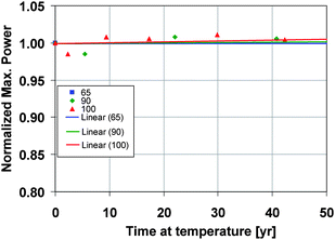
Since concentrator solar cells lack predictability of long-term field operation, a calculation from accelerated test data was made in an attempt to establish a correlation between cell performance and time of operation. Fig. 23 shows a prediction of the behavior of the normalized power for a C1MJ 3-junction concentrator solar cell as a function of time (in years) for operation at the 3 temperatures. These temperatures are indicative of CPV that would work with a passively-cooled system configuration. A low amplitude cyclical pattern in the data is observed and therefore the simplest way to predict their behavior is to use a straight line fit. Within the framework of the conditions used to generate these data, long term operation of this device structure should occur without any serious impediments as long as the solar cell is not physically damage from contact with an object. More data like this is imperative to build additional knowledge of CPV system predictability in the field under different environmental conditions.
 | ||
| Fig. 23 Power performance prediction from a 3-junction concentrator solar cell at 3 temperatures that are likely to occur in a CPV system during operation in the field. | ||
8 Conclusions and future outlook for CPV
Comparing to the existing level of maturity of Si technology in the PV industry, it could be said that multijunction CPV from III–V semiconductors could be in its early stages of development. In contrast, multijunction CPV has gone through extensive device performance improvements and gruelling qualifications tests which have catapulted prototype designs out from the laboratory into the field in just a few years. From these, there are several material systems that have been candidates for producing next-generation high efficiency solar cells. Metamorphic structures, for example, have been receiving considerable attention since the solar cell that set the new efficiency record of 40.8% was based on this material system but of equal importance is the lattice-matched system. In the last 8 years, solar cells built from these material systems have shared and enjoyed record-breaking efficiencies, and it is likely that this pace will continue in the coming years since there is, however, still more room for further refinements in the device structure, and their manufacturing methods.A parameter that influences multijunction cell production, and therefore impacting the overall CPV system feasibility is cost. Throughout this review, some points were touched upon regarding costs. For the end-user to take advantage of CPV-generated electricity, the overall installed systems costs must be minimized so that delivering power to the meter is affordable. In terms of cost breakdown, this means that the cell, module assembly, inverter and installations must all be reduced, each presently corresponding to about US $3/W, $2/W, $1/W and $3/W, respectively. The CPV roadmap rolled out by the solar initiative programs, which are federally-funded solar energy technologies program, is targeting installed systems to be $3–5/W by 2015, equating to localized cost of electricity (LCOE) of 7–8 ¢/kWh. Then, a likely scenario for the above cost breakdown (in the same order presented above) based on this LCOE using multijunction CPV would be 50¢/W, $1/W, $1/W and $1.5/W; with the last term selected quite aggressively. This is assuming that cell cost per area of wafer processed is $3–5/cm2, and commercial device efficiencies are 36%–40%. There is a good chance these cost objectives can be achieved ahead of time considering the present rate of success from some system component manufacturers. As a matter of fact, volume production of multijunction solar cells at Spectrolab is now costing slightly less than $1/W.
Companies abroad are working toward this goal. As an example, a few companies are currently targeting CPV for commercial introduction in the utilities market and remote areas for off-grid power generation. Triple junction solar cells made from GaInP/GaInAs/Ge are being used in dense array systems in Australia by Solar Systems PTY which is developing 33 kW CPV systems using these cells which will possibly enhance or displace their Si technology. When operating under concentrated sunlight, a multijunction CPV system with much less solar cell area than cells in a Si or in a thin film panel generates almost twice as much power.83 Just like in the dense array business, there is a market for point-focus systems which is also honing in on installations at the utility scale. Amonix, another manufacturer of CPV in the US is currently evaluating 3-junction solar cells for possible use in their Si-based, 25 kW, point-focus system for deployment to take place in the near future. Companies in other countries, primarily in Europe, such as Germany and Spain, are also making strides toward developing and expanding CPV.17,18,84 Concentrix Solar, for example, has recently deployed its CX5000 system using 3-junction cells capable of generating 5.75 kW.85 As of this writing, Concentrix has installed 300 kW of CPV. Further, demonstration projects are now underway at the Castilla La Mancha test site in Spain where a group of CPV companies have gathered to install their systems; an effort sponsored by ISFOC (Instituto de Sistemas Fotovoltaicos de Concentración or Institute of Photovoltaic Systems under Concentration) to install up to 3 MW of CPV for pilot power plant programs.86
There is much momentum in the solar PV field, and it is moving in a positive direction. Right now there is an upsurge in the amount of PV produced in the world due to many incentive programs, capital investment and cost reduction. Cell volume production has increased as a result of this growth, and more companies have entered this market to reap the benefits that others are currently gathering. It is expected that the annual electricity delivered to the consumer in the globe will reach tens of GW (109 Watts), with a substantial portion produced from perhaps 45% to even 50% high-efficiency multijunction CPV, in the years ahead. Hopefully, this will be the beginning to topple fossil fuel-burning which is responsible for climate change.
References
- C. Nedler, Market Outlook Part 2: Energy. Skyrocketing Fossil Fuel Prices Favor Renewables, Energy Capital Newsl., 2008, Energy and Capital, http://www.energyandcapital.com/articles/market-outlook-energy/655, (April, 2008) Search PubMed.
- J. L. Swain, Another Sunny Year for Solar Power, Vital Signs Online 2008, Worldwatch Institute, http://www.worldwatch.org/node/5449, September, 2008; J. G. Dorn, Solar Cell Production Jumps 50 Percent in 2007, Eco-Economy Indicators, 2007, Earth Policy Institute, http://www.earth-policy.org/Indicators/Solar/2007.htm (April, 2008) Search PubMed.
- Y. Zhao, Renewable Energy: China, Special Unit for South-South Cooperation V8, 2002, ch. 3, pp. 28–34, United Nations Development Programme,http://tcdc.undp.org/sie/experiences/vol8/China.pdf (August, 2008) Search PubMed.
- R. Wiser and G. Barbose, Renewables Portfolio Standards in the United States, 2008, pp. 12–20, Lawrence Berkeley National Laboratory,http://eetd.lbl.gov/ea/ems/reports/lbnl-154e.pdf (August, 2008) Search PubMed.
- C. Hammerle, 21st European Photovoltaic Solar Energy Conference, 2006, pp. 2631–2633 Search PubMed.
- Trends in Photovoltaic Power Systems, IEA–PVPS T1–16, 2007, pp. 28–32, Photovotaic Power Systems Programme, International Energy Agency, http://www.iea-pvps.org/products/download/rep1_16.pdf (August, 2008) Search PubMed.
- R. Leutz, Management of growth: Concentrating Photovoltaics, February, 2008, Renewable Energy World, http://www.renewableenergyworld.com/rea/news/reworld/story?id = 51589 (August, 2008) Search PubMed.
- Solar Indicator Data, 2007, Earth Policy Institute, http://www.earthpolicy.org/Indicators/Solar/2007_data.htm#fig3 (August, 2008) Search PubMed.
- P. Maycock and T. Bradford, PV market update: Demand grows quickly and supply races to catch up, July, 2007, Renewable Energy World, http://www.renewableenergyworld.com/rea/news/story?id=51484 (August, 2008) Search PubMed.
- 2007 World PV Industry Report Highlights, Marketbuzz, Solarbuzz, http://www.solarbuzz.com/Marketbuzz2008-intro.htm ( March, 2008) Search PubMed.
- Global Market Outlook for Photovoltaics until 2012: Facing a Sunny Future, European Photovoltaic Industry Association, 2007, http://www.epia.org/fileadmin/EPIA_docs/publications/epia/EPIA__MarketPublication_18feb.pdf Search PubMed.
- International Energy Outlook 2008: Highlights, Energy Information Administration, http://www.eia.doe.gov/oiaf/ieo/highlights.html ( April, 2008) Search PubMed.
- Projects, http://www.eia.doe.gov/oiaf/ieo/highlights.html ( August, 2008) Search PubMed.
- Installation Examples, http://www.amonix.com/Amonix_Installation_Examples.html ( August, 2008) Search PubMed.
- Phase One of Planned 3-MW SolFocus CPV Plant Ready To Go Online, July 2008, Renewable Energy World, http://www.amonix.com/Amonix_Installation_Examples.html (August, 2008) Search PubMed.
- P. J. Verlinden, A. Lewandowski, C. Bingham, G. S. Kinsey, R. A. Sherif and J. B. Lasich, 4th IEEE World Conference on Photovoltaic Energy Conversion, 2006, pp. 592–597 Search PubMed.
- A. Hakenjos, J. Wüllner and H. Lerchenmüller, 22nd European Photovoltaic Solar Energy Conference, 2007, p. 156 Search PubMed.
- A. W. Bett, B. Burger, F. Dimroth, G. Siefer and H. Lerchenmüller, IEEE 4th World Conference on Photovoltaic Energy Conversion, 2006, pp. 615 – 620 Search PubMed.
- S. M. Bedair, M. F. Lamorte and J. R. Hauser, Appl. Phys. Lett., 1979, 34, 38–40 CrossRef CAS; J. A. Hutchby, R. J. Markunas, and S. M. Bedair, 14th Critical Reviews of Technology Conference, Society of Photo-Optical Instrumentation Engineers, 1985, pp. 40–61 Search PubMed.
- G. F. Virshup, B.-C. Chung and J. G. Werthen, 20th IEEE Photovoltaic Specialists Conference, 1988, pp. 441–445 Search PubMed.
- J. M. Olson, T. Gessert and M. Al-Jassim, 18th IEEE Photovoltaic Specialists Conference, 1985, pp. 552–555 Search PubMed.
- J. Olson, S. Kurtz, A. Kibbler and P. Faine, Appl. Phys. Lett., 1990, 56, 623–625 CrossRef CAS.
- K. A. Bertness, S. R. Kurtz, D. J. Friedman, A. E. Kibbler, C. Kramer and J. M. Olson, Appl. Phys. Lett., 1994, 65, 989–991 CrossRef CAS.
- M. Yamaguchi and S. Wakamatsu, 25th IEEE Photovoltaic Specialists Conference, 1996, p. 167 Search PubMed.
- H. L. Cotal, D. R. Lillington, J. H. Ermer, R. R. King, N. H. Karam, S. R. Kurtz, D. J. Friedman, J. M. Olson, J. S. Ward, A. Duda, K. A. Emery and T. Moriarty, 28th IEEE Photovoltaic Specialists Conference, 2000, pp. 955–960 Search PubMed.
- R. R. King, C. M. Fetzer, P. C. Colter, K. M. Edmondson, D. C. Law, A. P. Stavrides, H. Yoon, G. S. Kinsey, H. L. Cotal, J. H. Ermer, R. A. Sherif, K. Emery, W. Metzger, R. K. Ahrenkiel and N. H. Karam, 3rd World Conference on Photovoltaic Energy Conversion, Osaka, Japan, 2003, pp. 622–625 Search PubMed.
- R. R. King, C. M. Fetzer, K. M. Edmondson, D. C. Law, P. C. Colter, H. L. Cotal, R. A. Sherif, H. Yoon, T. Isshiki, D. D. Krut, G. S. Kinsey, J. H. Ermer, Sarah Kurtz, T. Moriarty, J. Kiehl, K. Emery, W. K. Metzger, R. K. Ahrenkiel and N. H. Karam, 19th European Photovoltaic Solar Energy Conference, Paris, France, 2004, pp. 3587–3593 Search PubMed.
- R. R. King, D. C. Law, C. M. Fetzer, R. A. Sherif, K. M. Edmondson, S. Kurtz, G. S. Kinsey, H. L. Cotal, D. D. Krut, J. H. Ermer and N. H. Karam, 20th European Photovoltaic Solar Energy Conference, Barcelona, Spain, 2005, pp. 118–123 Search PubMed.
- R. R. King, R. A. Sherif, D. C. Law, J. T. Yen, M. Haddad, C. M. Fetzer, K. M. Edmondson, G. S. Kinsey, H. Yoon, M. Joshi, S. Mesropian, H. L. Cotal, D. D. Krut, J. H. Ermer and N. H. Karam, 21st European Photovoltaic Solar Energy Conference and Exhibition, Dresden, Germany, 2006, pp. 124–128 Search PubMed.
- R. R. King, D. C. Law, K. M. Edmondson, C. M. Fetzer, G. S. Kinsey, H. Yoon, R. A. Sherif and N. H. Karam, Appl. Phys. Lett., 2007, 90, 183516 CrossRef.
- R. R. King, D. C. Law, K. M. Edmondson, C. M. Fetzer, G. S. Kinsey, D. D. Krut, J. H. Ermer, R. A. Sherif and N. H. Karam, 4th International Conference on Solar Concentrators, 2007.
- J. F. Geisz, D. J. Friedman, J. S. Ward, A. Duda, W. J. Olavarria, T. E. Moriarty, J. T. Kiehl, M. J. Romero, A. G. Norman and K. M. Jones, Appl. Phys. Lett., 2008, 93, 123505 CrossRef.
- K. Araki, M. Kondo, H. Uozumi, Y. Kemmoku, T. Egami, M. Hiramatsu, Y. Miyazaki, N. J. Ekins-Daukes, M. Yamaguchi, G. Seifer and A. B. Bett, 19th European Photovoltaic Solar Energy Conference, 2004.
- Solar America Initiative Photovoltaic Incubator, 2007, pp. 68–96, DOE Solar Energy Technologies Program Annual Report, http://www1.eere.energy.gov/solar/pdfs/fy07_annual_report.pdf (August, 2008) Search PubMed.
- G. S. Kinsey, R. A. Sherif, H. L. Cotal, P. Pien,. R. R. King, R. J. Brandt, W. G. Wise, E. L. LabiosK. F. Wan, M. Haddad, J. M. Lacey, C. M. Fetzer, P. Verlinden, J. Lasich and N. H. Karam, Proc. 4th World Conference on Photovoltaic Energy Conversion, 2006, pp. 625–627 Search PubMed.
- R. A. Sherif, S. Kusek, H. Hayden, R. King, H. L. Cotal, J. Peacock, M. Caraway and N. H. Karam, 31st IEEE Photovoltaic Specialists Conference, 2005, pp. 635–638 Search PubMed.
- A. L. Fahrenbruch and R. H. Bube, Fundamentals of Solar Cells, Photovoltaic Solar Energy Conversion, Academic Press, San Diego, 1983, pp. 308–311 Search PubMed.
- G. B. Stringfellow in Organometallic Vapor-Phase Epitaxy, Academic Press, San Diego, 2nd edn, 1999, ch. 1 Search PubMed.
- R. D. Dupius, IEEE J. Select Topic Quant. Electr. 2000, 6, pp. 1040–1050 Search PubMed.
- J. Nelson in Physics of Solar Cells, Imperial College Press, London, 2003, ch. 10.5, pp. 298–301 Search PubMed.
- S. M. Sze and K. K. Ng inPhysics of Semiconductor Devices, Wiley, Boston, 3rd edn, 2007, pp. 719–742 Search PubMed.
- A. Hadipour, B. D. Boer and P. W. M. Blom, Adv. Funct. Mater., 2008, 18, 169–181 CrossRef CAS.
- A. Yakimov and S. R. Forrest, Appl. Phys. Lett., 2002, 80, 1667 CrossRef CAS.
- J. M. Olson, S. R. Kurtz, A. E. Kibbler and P. Faine, Appl. Phys. Lett., 1990, 56, 623 CrossRef CAS.
- K. Seeger, Semiconductor Physics, An Introduction, Springer-Verlag, Berlin, 4th edn, 1988, pp. 270–276 Search PubMed.
- R. R. King, M. Haddad, T. Isshiki, P. Colter, J. Ermer, H. Yoon, D. E. Joslin and N. H. Karam, Proc. 28th IEEE Photovoltaic Specialists Conference, Anchorage, Alaska, 2000, pp. 982–985 Search PubMed.
- F. Dimroth, U. Schubert and A. W. Bett, IEEE Electron Dev. Lett., 2000, 21(5), 209 CrossRef CAS.
- J. C. Schultz, M. E. Klausmeier-Brown, M. Ladle Ristow and M. M. Al-Jassim, 21st IEEE Photovoltaic Specialists Conference, 1990, pp. 148 Search PubMed.
- M. W. Wanlass, S. P. Ahrenkiel, R. K. Ahrenkiel, D. S. Albin, J. J. Carapella, A. Duda, J. F. Geisz, S. Kurtz, T. Moriarty, R. J. Wehrer and B. Wernsman, 31st IEEE Photovoltaic Specialists Conference, 2005, pp. 530–535 Search PubMed.
- J. F. Geisz, Sarah Kurtz, M. W. Wanlass, J. S. Ward, A. Duda, D. J. Friedman, J. M. Olson, W. E. McMahon, T. E. Moriarty and J. T. Kiehl, Appl. Phys. Lett., 2007, 91, 023502 CrossRef.
- R. R. King, D. E. Joslin and N. H. Karam, Multijunction Photovoltaic Cell with Thin 1st (Top) Subcell and Thick 2nd Subcell of Same or Similar Semiconductor, US Pat. 6 316 715, 2001 Search PubMed.
- R. R. King, P. C. Colter, D. E. Joslin, K. M. Edmondson, D. D. Krut, N. H. Karam and Sarah Kurtz, High-Voltage, Low-Current GaInP/GaInP/GaAs/GaInNAs/Ge Solar Cells, 29th IEEE Photovoltaic Specialists Conference, New Orleans, Louisiana, 2002, pp. 852–855 Search PubMed.
- R. R. King, D. C. Law, K. M. Edmondson, C. M. Fetzer, G. S. Kinsey, H. Yoon, D. D. Krut, J. H. Ermer, R. A. Sherif and N. H. Karam, Adv. Optoelectr., 2007 DOI:10.1155/2007/29523.
- D. J. Friedman, J. F. Geisz, A. G. Norman, M. W. Wanlass and S. R. Kurtz, 4th IEEE World Conference on Photovoltaic Energy Conversion, 2006, vol. 1, pp. 598–602 Search PubMed.
- F. Dimroth, C. Baur, A. W. Bett, M. Meusel and G. Strobl, 31st IEEE Photovoltaic Specialists Conference, 2005, p. 525; A. Bett, Multijunction Solar Cells in Europe, 2007, http://re.jrc.ec.europa.eu/solarec/events/0511fullspectrum/2_2_Bett.pdf (August, 2008) Search PubMed.
- A. J. Ptak, D. J. Friedman, S. Kurtz and J. Kiehl, 31st IEEE Photovoltaic Specialists Conference, 2005, pp. 603–606 Search PubMed.
- J. E. Avery, L. M. Fraas, V. S. Sundaram and N. Manssori, 21st IEEE Photovoltaic Specialists Conference, 1990, p. 1277 Search PubMed.
- L. M. Fraas, W. E. Daniels, H. X. Huang, L. E. Minkin, J. E. Avery, C. Chu, P. Lies, M. J. O'Neill,A. J. McDanal and M Piszczorike, NASA Report, 2002, pp. 24–31 Search PubMed.
- J. C. C. Fan, B.-Y. Tsaur and B. J. Palm, 16th IEEE Photovoltaic Specialists Conference, 1982 Search PubMed.
- V. M. Andreev, V. M. Lantratov, V. R. Larionov, V. D. Rumyantsev and M. Z. Shvarts, 25th IEEE Photovoltaic Specialists Conference, 1996, pp. 341–344 Search PubMed.
- M. W. Wanlass, J. S. Ward, T. A. Gessert, K. A. Emery, G. S. Horner, T. J. Coutts, G. F. Virshup and M. L. Ristow, 21st IEEE Photovoltaic Specialists Conference, 1990, pp. 172–178 Search PubMed.
- D. R. Lillington and D. E. Joslin, High Efficiency Multijunction Solar Cells, US Pat. 5 853 497, 1998 Search PubMed.
- W. Blocker, Proc. IEEE, 1978, 66, 104 CrossRef.
- R. L. Moon, L. W. James, H. A. Vander Plas, T. O. Yep, A. Antypas and Y. Chai, 13th IEEE Photovoltaic Specialist Conference, 1978, p. 859 Search PubMed.
- A. Barnett, D. Kirkpatrick, C. Honsberg, et al., 22nd European Photovoltaic Solar Energy Conference, 2007 Search PubMed.
- S. M. Sze in Physics of Semiconductor Devices, Wiley, New York, 2nd edn, 1981, pp. 245–311 Search PubMed.
- F. Ren, A. B. Emerson, S. J. Pearton, W. S. Hobson, T. R. Fullowan and J. Lothian, J. Electr. Mater., 1991, 20, 595 Search PubMed.
- O. Wada, S. Yanagisawa and H. Takanashi, Appl. Phys. Lett., 1976, 29, 263–265 CrossRef CAS.
- A. Lahav, M. Eizenberg and Y. Komem, J. Appl. Phys., 1986, 60, 99 CrossRef.
- C. Nuhoglu, M. Saglam and A. Türüt, Semicond. Sci. Technol., 1999, 14, 114–117 CrossRef CAS.
- J. R. Waldrop, Appl. Phys. Lett., 1982, 42, 350 CrossRef.
- J. R. Waldrop, Appl. Phys. Lett., 1984, 44, 1002 CrossRef CAS.
- K. A. Jones, M. W. Cole, W. Y. Han, D. W. Eckart, K. P. Hilton, M. A. Crouch and B. H. Hughes, J. Appl. Phys., 1997, 82, 1723 CrossRef CAS.
- J. M. O. Zide, A. Kleiman-Schwarsctein, N. C. Strandwitz, J. D. Zimmerman, T. Steenblock-Smith, A. C. Gossard, A. Forman, A. Ivanovskaya and G. D. Stucky, Appl. Phys. Lett, 2006, 88, 162103 CrossRef.
- S. J. Pearton in Wide Band Gap Semiconductors, William Andrew, Salem, 1999, pp. 98–150 Search PubMed.
- A. W. Bett, F. Dimroth, G. Lange, M. Meusel, R. Beckert, M. Hein, S. V. Riesen and U. Schubert, 28th IEEE Photovoltaic Specialists Conference, 2000, pp. 961–964 Search PubMed.
- C. Algora, E. Ortiz, I. Rey-Stolle, V. Díaz, R. Peña, V. M. Andreev, V. P. Khvostikov and V. D. Rumyantsev, IEEE Trans. Electr. Dev., 2001, 48, 840 Search PubMed.
- H. J. Hovel, Semiconductor and Semimetals, Academic Press, New York, 1975, ch. 2, pp. 8–46 Search PubMed.
- C. H. Henry, J. Appl. Phys., 1980, 51, 4494–4500 CrossRef CAS.
- C. Algora, Very High Concentration Challenges of III–V Multijunction Solar Cells, Springer-Verlag, Berlin, ed. Luque and Andreev, 2007, ch. 5, pp. 89–111 Search PubMed.
- W. E. McMahon, K. E. Emery, D. J. Friedman, L. Ottoson, M. S. Young, J. S. Ward, C. M. Kramer, A. Duda and Sarah Kurtz, Prog. Photovoltaics: Res. Appl., 2007, 16, 213–214 Search PubMed.
- G. S. Kinsey, P. Hebert, K. E. Barbour, D. D. Krut, H. L. Cotal and R. A. Sherif, Prog. Photovoltaics: Res. Appl., 2008, 16, 1–6 Search PubMed.
- M. Yamaguchi, T. Takamoto and K. Araki, Sol. Energy Mater. Sol. Cells, 2006, 90, 3068–3077 CrossRef CAS.
- S. R. Kurtz, Opportunities and Challenges for Development of a Mature Concentrating Photovoltaic Power Industry, Technical Report NREL/TP-520–43208, National Renewable Energy Laboratory, 2007, pp. 1–16, http://www.nrel.gov/pv/pdfs/43208.pdf ( August, 2008) Search PubMed.
- H. Lerchenmüller, A. Hakenjos, I. Heile, B. Burger and O. Stalter, International Conference on Solar Concentrators for the Generation of Electricity or Hydrogen, 2007 Search PubMed.
- About ISFOC, ISFOC, http://www.isfoc.es/ ( August, 2008) Search PubMed.
| This journal is © The Royal Society of Chemistry 2009 |