Multifunctional 3D nanoarchitectures for energy storage and conversion†
Debra R.
Rolison
*a,
Jeffrey W.
Long
*a,
Justin C.
Lytle
a,
Anne E.
Fischer
b,
Christopher P.
Rhodes
c,
Todd M.
McEvoy
d,
Megan E.
Bourg
a and
Alia M.
Lubers
a
aSurface Chemistry Branch, Code 6170, US Naval Research Laboratory, Washington, DC 20375, USA
bNova Research, Inc., 1900 Elkin Street, Suite 230, Alexandria, VA 22308, USA
cLynntech, Inc., College Station, TX 77840, USA
dAir Products and Chemicals, Inc., 7201 Hamilton Boulevard, Allentown, PA 18195, USA
First published on 17th November 2008
Abstract
The design and fabrication of three-dimensional multifunctional architectures from the appropriate nanoscale building blocks, including the strategic use of void space and deliberate disorder as design components, permits a re-examination of devices that produce or store energy as discussed in this critical review. The appropriate electronic, ionic, and electrochemical requirements for such devices may now be assembled into nanoarchitectures on the bench-top through the synthesis of low density, ultraporous nanoarchitectures that meld high surface area for heterogeneous reactions with a continuous, porous network for rapid molecular flux. Such nanoarchitectures amplify the nature of electrified interfaces and challenge the standard ways in which electrochemically active materials are both understood and used for energy storage. An architectural viewpoint provides a powerful metaphor to guide chemists and materials scientists in the design of energy-storing nanoarchitectures that depart from the hegemony of periodicity and order with the promise—and demonstration—of even higher performance (265 references).
 Debra Rolison | Debra Rolison heads the Advanced Electrochemical Materials section at the US Naval Research Laboratory (NRL) where she and her team specialize in designing and creating multifunctional nanoarchitectures for rate-critical applications, including energy storage and conversion. She is a Fellow of the AAAS, MRS, and AWIS, and a noted activist on issues affecting women in science. |
 Alia Lubers, Jeffrey Long, and Megan Bourg | Jeffrey Long is a staff scientist in the Surface Chemistry Branch at the NRL where his research centers on the development of nanostructured materials for electrochemical power sources and separation/filtration. He received a PhD in Chemistry from the University of North Carolina in 1997 and a BS from Wake Forest University in 1992. |
 Justin Lytle | Justin Lytle was a research fellow at the NRL from 2005–2008, where he developed electrode nanoarchitectures as 3D scaffolds for catalytic nanoparticles and conformal, ultrathin electrodes and solid-state electrolytes. He received his PhD in Chemistry at the University of Minnesota (2005) working with Andreas Stein. He is presently an assistant professor of chemistry at Pacific Lutheran University. |
 Anne Fischer, Christopher Rhodes, and Todd McEvoy | Anne Fischer (PhD in Chemistry, Michigan State University, 2005) is currently an AAAS Science & Technology Policy Fellow at the National Science Foundation and senior scientist with Nova Research, Inc. Her research interests include materials development for energy storage devices. |
Christopher Rhodes (PhD in chemistry from University of Oklahoma, 2001) did a joint postdoctoral at UCLA and the NRL from 2002–2005. He is now a Research Scientist at Lynntech, Inc., where he develops advanced nanostructured electrodes and solid-state electrolytes. |
Todd McEvoy received his PhD in Chemistry from the University of Texas at Austin in 2003. After a postdoctoral at the NRL, he joined Air Products and Chemicals where he develops materials for use in lithium-ion batteries, organic light-emitting diodes and photovoltaics. |
Megan Bourg received a BS in Chemistry from Southwestern University (2001) and a PhD in Chemistry from the University of California, Irvine (2007). Now a National Research Council postdoctoral fellow at the NRL, she is using her electrochemical skills to design and characterize 3D hybrid nanostructures for applications in electrical energy storage under the direction of Dr. Jeffrey Long. |
Alia Lubers is a senior undergraduate in chemical engineering at Carnegie Mellon University. She spent 2008 interning at the NRL where she fabricated and electrochemically investigated catalytic nanomaterials for energy-conversion applications. |
1. Introduction
Electrochemistry—the word and the science—embodies the interplay of two inseparable physicochemical driving forces: chemical potential (μc) and the work associated with moving a charged particle, as evidenced by the key governing equation for electrochemical potential (μec):| μec = zFϕ + μc |
At the heart of all electrochemical phenomena lies matter undergoing charge-transfer reactions. Electrochemistry successfully achieves the synthesis or analysis or decomposition of matter, but when the electrochemical goal is to make electronic or ionic charge do the work of batteries, electrochemical capacitors, fuel cells, and photovoltaics, the necessary interaction of the physical with the chemical is rarely achieved such that all reactants express optimal mobility and reactivity. All four of these electrochemical power sources share a common set of components: opposing electrodes—one with a surface excess of electrons (cathode), the other with a deficit (anode). Yet this apparent simplicity masks a complex physicochemical reaction environment.
The electrochemistry that yields the electrons per second that power our electronic devices or distributed sensors originates in a nanoscopic zone where reaction kinetics and the movement of matter, electronic charge, and ionic charge must cooperate simultaneously. The multifunction required for storage or generation of electrochemical energy is also an indissoluble blend of physics and chemistry and can be likened to the three-phase boundary that governs reactivity in heterogeneous catalysis, including the electrocatalysis that drives fuel cells. As seen in Fig. 1 for carbon-supported nanoparticulate Pt electrocatalysts,2,3 the carbon black serves as an ad-hoc agglomerated wire that moves the electrons generated by oxidation of the hydrogen fuel out of the cell to power the device (the “load”). But for the electrons to do work (i.e., power the device), concomitant physical, chemical, and electrochemical processes must occur: transport of molecular hydrogen to the carbon-supported Pt nanocatalyst; adsorption of hydrogen at the Pt surface; electro-oxidation of fuel to protons, governed by the reaction kinetics inherent to nanoscopic Pt; and movement of protons out of the nanophasic volume via a proton-conducting medium (which is not Pt or carbon, but a liquid electrolyte or ionomeric strong-acid polymer). For the fuel cell to function, all of these elementary processes must be mirrored at the cathode for reduction of the oxidant.
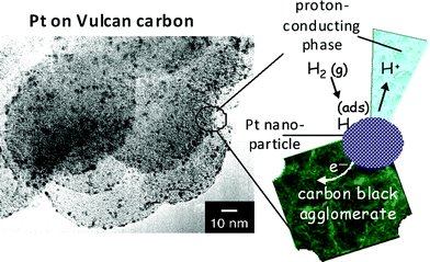 | ||
| Fig. 1 The active intersection of functionality at the three-phase boundary of a carbon-supported Pt electrocatalyst. To electrogenerate power (electrons per second at a specific potential), the reactive interphase requires transport of a gas-phase reactant (H2 in this example) to and adsorption at a Pt nanoparticle while maintaining intimate contact to a proton-conducting phase (such as an acid electrolyte or a proton-exchange polymer). (Micrograph is reproduced from ref. 3; reprinted with permission. Copyright 2002, American Chemical Society.) | ||
The three-phase boundary where all the necessary reactants—molecules, electrons, ions, and reactive surfaces—jam together to perform the multifunctional electrochemistry that yields energy, represents a fractional component, often a minor fractional component, of the total volume of the electrode structure. Even in the phase conversion inherent to energy storage in batteries, one must coordinate mass transport, charge transport (i.e., electronic and ionic mobility), and electron-transfer kinetics in order to store or release energy. And independent optimization of the elementary processes that give rise to the various forms of energy-relevant functionality is difficult with bulk materials.
Designing an optimal physical space for this vital energy intersection is nontrivial with so much countervailing multifunctionality at work: electrons prefer order for high mobility; ions need space, i.e., atomic-level vacancies and some measure of disorder are necessary for transport over any distance at reasonable rates; molecules need either room to move at length scales on the order of tens of nanometers or high solubility in a condensed phase. Little wonder that a Moore’s Law, with a doubling of performance at half the cost every two years, does not govern energy storage or conversion. In the critical market of Li-ion batteries—the portable power keeping laptops and numerous other consumer electronics humming—performance improves at a rate of ∼10% per year.4,5
1.1 Controlling functionality on the nanoscale in three dimensions
Electrochemical energy technologies underpin any future success in the global effort to divert energy usage away from carbon-laden fuels, whether one considers storage in batteries and electrochemical capacitors (ECs) or alternative production, such as with photovoltaics or fuel cells run with sustainably derived hydrogen.As seen in Fig. 2,6 the often orthogonal demands of energy vs. power density are satisfied by selecting particular technologies to meet energy density (at the expense of power density) and vice versa. Devices with high power needs turn to interfacial storage of charge such as in dielectric capacitors and the double-layer equivalent characteristic of electrochemical capacitors. As energy density becomes the key operational requirement, the electrochemical power source choices are batteries, and with the ability to refuel the power source, fuel cells. Marked improvement in the performance of electrochemical power sources is critical, especially as focused on simultaneously improving energy and power density.
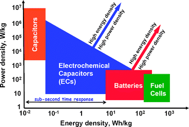 | ||
| Fig. 2 Comparison of the operational characteristics of energy storage and conversion devices indicating the desire to improve both energy density and power density for batteries and electrochemical capacitors. (Adapted from ref. 5.) | ||
But with technologies as mature as batteries and fuel cells, a shift in focus—in our view, a shift in dimensionality—is required to move to a new performance growth curve.7,8 We and other groups around the world are rethinking the requisite multifunction—mass transport, electronic and ionic conductivity, electron-transfer kinetics—in light of architectural design in three dimensions,9 including the design and fabrication of three-dimensional multifunctional architectures from the appropriate nanoscale building blocks, with the use of “nothing” (void space) and deliberate disorder as design components.10,11
1.2 Skyscraper vs. ranch house
Surveying electrochemical power from an architectural viewpoint offers a powerful metaphor to guide the (electro)chemist and materials scientist in the design of nanoarchitectures and in their physical and chemical transformation into multifunctional objects that yield high performance for energy storage and conversion.11 While the simplicity of 2D designs is desirable for cost-effective mass production in which layers of functionality are built up, 2D electrochemical cells are fundamentally limited in the amount of energy that they can store and the amount of power that they can deliver per unit area, mass, and volume.In contrast, electrochemical interfaces that are interpenetrated in 3D offer major gains in energy and power density, especially with respect to the geometric footprint of the device. In particular, small devices cannot spare the square footage necessary for a thin-film 2D battery or electrochemical capacitor to provide the energy sufficient for the anticipated demands on the device.8,9 The ability to minimize the geometric footprint while retaining internal square footage of usable function is shown analogously in Fig. 3, contrasting the Burj Dubai skyscraper with 28% of the areal footprint but more than three times the square footage of Hershey’s Eastern Distribution plant. Transitioning these architectural lessons to energy storage devices affords significant and simultaneous gains in energy and power density.
 | ||
| Fig. 3 Contrasting the footprint of 2D (the Hershey Eastern Distribution Center, Hershey, PA) with the increase in square footage by designing in 3D (the Burj Dubai under construction). | ||
1.3 3D designs—advantages and disadvantages
The recent advances in creating mesoscopic structures and devices, including microelectromechanical systems (MEMS) and distributed sensors such as smart dust,12–14 have not been accompanied by comparable advances in down-sizing their on-board source of power. Because such devices do not impose a high load on the power source, microbatteries can be devised that are not the ultimate in capacity or power density, which also permits more freedom in design. A redesign from 2D to 3D yields a solid-state battery in which all active components—anode, cathode, and physical separator/ionically conductive phase—are potentially within nanometers of one another (Fig. 4), yet can be scaled up (literally up) to meet the desired energy density. A qualitative comparison between 2D and 3D microbatteries can be found in Table 1.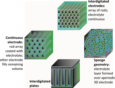 | ||
| Fig. 4 Three-dimensional designs for batteries. (Adapted from ref. 8; reprinted with permission. Copyright 2004, American Chemical Society.) | ||
| Solid-state ion diffusion pathlength | Effective active mass utilization | Energy density | Power density | Areal footprint | |
|---|---|---|---|---|---|
| 2D thin film | >1 μm | Low | High | Moderate | Large |
| 3D nanoarchitectures | <100 nm | High | Moderate | High | Small |
The prime advantages one expects with the proposed 3D architectures for energy storage in batteries, in addition to the small areal footprint, are the short transport lengths for ions in the solid-state electrode as well as between the anode and cathode. That the 3D design minimizes both distances yields concomitant improvements in power density. If the nanoarchitectured electrodes are highly conductive, extension of the length (scaling in the z direction) also improves the energy density; but as most insertion oxides are not highly conductive, the ohmic drops that occur at the segments of the electrode far from the current collector must be factored into any 3D design.7–9
Aerogels and ambigels comprise one class of porous, aperiodic sponge geometry (Fig. 4) that innately builds in solid wires for charge transport and 3D plumbing for molecular transport.15 These nanoarchitectures are sol–gel-derived ultraporous materials processed from the wet gels such that the pore network stays through-connected and constitutes a synthesis-controlled volume fraction of 75–99.9%.16 Ambigels result when wet gels are dried under conditions where the capillary forces are minimized (e.g., from nonpolar liquids with low surface tension)15 and aerogels result when wet gels are dried such that no capillary forces are established (e.g., by supercritical fluid extraction).16
These ultraporous solids unite high surface area for heterogeneous reactions with a continuous, porous network for rapid diffusional flux of reactants/analytes/substrates to internal surfaces, and do so over length scales from tens of nanometers to meters.10,11,15,16 Response times to gas-phase analytes are >10 times faster than those of the same chemistry expressed in a standard sol–gel-derived material such as a xerogel.17,18
Because the name-of-the-game in batteries is capacity at high cell voltage, aerogels (which are mostly nothing) would not seem to be the first choice of matter with which to construct a new battery. An architectural perspective, however, yields a different assessment. Aerogel-like objects are scaffolds that provide self-wired ∼10-nm thick electrodes (the solid network) co-continuous with the 3D-interconnected pore network (i.e., high-quality plumbing) necessary to introduce the molecular or particulate reagents that impart the additional functionality required to create a battery or electrochemical capacitor or fuel cell or solar cell.
One way to construct a 3D battery is to synthesize the intercalating cathode as a metal oxide nanoarchitecture. The operative reactions by which energy is stored in a key battery-relevant insertion oxide, manganese dioxide of alkaline batteries (H+ insertion) and Li-ion batteries, relies on a dual insertion reaction of cation and electron:
| MnIVO2 + x e− + x H+→ HxMnIIIxMnIV1−xO2 |
| MnIVO2 + x e− + x Li+→ LixMnIIIxMnIV1−xO2. |
The expected 3D advantages accompany the architectural layout of a sponge/aerogel-like energy reactor, but so do fabrication challenges. Pinhole-free coating of the surface of the networked, nanoscale electrode will be required to provide separator functionality. Interesting questions then arise: if the coating is less than perfect, will short circuits result? If so, will short circuits be localized? (because of the nanoscopic nature of the components) or all-consuming? (because of the continuous nature of the networked oxide domains and the through-connected mesoporous volume). Our instinct currently suggests that the shorts will self-limit. We expect the mechanical properties of the polymer to confer a more elastic Young’s modulus to the interphase between the oxide cathode and the infiltrated anode, thereby helping to minimize mechanical stresses that arise with cycling. In addition, the nanoscopic nature of the insertion materials should also lessen the detrimental physical stresses that arise during charge–discharge cycling of the oxide.
We now turn to the specifics of designing, creating, characterizing, and integrating the multifunctional components necessary to construct electrochemical capacitors, 3D microbatteries, fuels cells, and even photovoltaics.
2. Importance of self-limiting processes in 3D architectures
The chemical or physical methods used to modify the interior and exterior of an electrode architecture to introduce desired functionality, reactivity, and stability are reactions that occur in a confined volume, not an open, line-of-sight, high flux, reactant-flooded environment. A high-quality void volume, most particularly a fully interconnected 3D pore structure facilitates solvent infiltration, ion transport, and reactant/byproduct mass transport. The nature of the “nothing”—the void volume of the structure—is the key design component in achieving high-quality modification of the interior of 3D architectures, especially as pore size drops below 100 nm.The critical step when using deposition to generate ultrathin (<100 nm), conformal films or coatings within 3D electrically conductive nanoarchitectures is to rely on self-limiting reactions, as shown in Fig. 5. Upon initiating deposition, the precursor initially reacts at the boundary of the porous electrode structure. A concentration gradient immediately arises that initiates diffusion of precursor from the bulk medium to the boundary and the internal volume of the electrode. As illustrated in Fig. 5(a), under conventional deposition conditions, the gradient results in preferential reaction of precursor at the outer boundary of the 3D electrode. Such localized deposition essentially paves over the boundary envelope of the porous electrode, thereby entombing the internal pore volume and internal electrode interfaces with detrimental consequences for electrochemical applications. In contrast, under self-limiting deposition conditions, the thickness of the film is constrained (Fig. 5(b)). The result is deposition of a conformal, uniform coating at all reactive interfaces throughout the continuous pore network of the ultraporous, 3D structure.
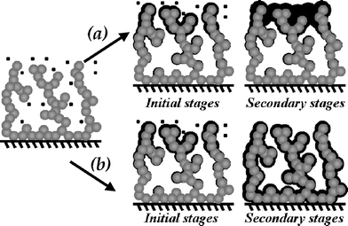 | ||
| Fig. 5 Schematic representation of film deposition within an ultraporous 3D structure that illustrates (a) the loss of accessible pore volume that occurs using conventional techniques and (b) the conformal, ultrathin coating on external and internal interfaces under conditions that are self-limiting. | ||
Several methodologies exist for the deposition of thin films in 3D structures and effectively overcome some of the limitations associated with conventional, planar, 2D approaches, but none are without design challenges. Some techniques (e.g., vapor deposition routes, including atomic-layer deposition (ALD),19 vapor-deposition polymerization (VDP),20,21 and molecular-layer deposition (MLD),22 can be limited by the need to maintain and operate elaborate deposition equipment. Photopolymerization approaches have shown merit for creating 3D objects,23,24 but the technique is impractical to conformally coat 3D nanoarchitectures in a controlled, ultrathin manner. In the following sections we describe modification protocols that have shown or may show promise for modifying the internal surfaces of 3D nanoarchitectures.
2.1 Layer-by-layer deposition
An expanding array of nanotechnological applications in catalysis, drug delivery, sensing, biomaterials, and separations is being driven by layer-by-layer (LbL) deposition.25,26,27 This process first introduced in 199128 offers one potential approach to conformally coat in 3D and within nanoarchitectures. Briefly, LbL deposition is initiated by electrostatically binding a charged polymer with an oppositely charged surface.29 Multiple polymer layers are subsequently assembled by alternately immersing the substrate in positively and negatively charged polymeric solutions, where charge neutrality within a layer is maintained by a nonpolymeric univalent counterion.30 What results on planar substrates is a stacked structure of well-controlled thickness,29 albeit with a less than sharply defined molecular interface between the polyelectrolyte anionic and polyelectrolyte cationic layers. Other forces such as hydrogen bonding, hydrophobic interactions, and covalent bonding have also been exploited to achieve LbL control.29Control of the surface energetics of deposited polyelectrolyte films is critical in order to tune the transport of molecular and ionic species in battery and fuel cell devices. Poly(diallyl dimethyl ammonium chloride)/sulfonated poly(2,6-dimethyl-1,4-phenylene oxide) (PDAC/sPPO) diminishes methanol permeation through Nafion membranes by two orders of magnitude, improving the faradaic efficiency of oxygen reduction at DMFC cathodes.31Polyelectrolyte films can also be deposited as Li-ion permeable membranes that conform to electrode arrays32,33 including viral particle templates.34
Ultrathin films of electroactive polymers deposited viaLbL deposition onto planar substrates have been demonstrated recently. Ge et al. reported the deposition of electroactive polyaniline films, with approximate monolayer-level control of electrode thickness, as well as ultrathin (<5-nm thick) bilayer films of polyaniline and poly(acrylic acid) on planar indium–tin oxide substrates.35
Deposition within ultraporous 3D architectures with LbL is more difficult, and consequently, far less well established. Uniform 3D coatings from colloidal dispersions can be achieved with carefully controlled LbL methods,28,36 although the permeability of the resulting colloidal assemblies is not always known. Polymer microtubules,37,38nanotubes,39–41 nanofibers,41 and other 3D structures have been created viaLbL templating methods.25–28 Many of these approaches involve uniform porous templates such as membranes with cylindrical pores, and relatively few examples exist for LbL deposition in heterogeneous, porous structures with tortuous interior pathways and pores on the order of 50–300 nm.27
2.2 Self-assembly
Colloidal particles can modify electrochemical interfaces in a self-limiting fashion under tightly controlled conditions that balance the repulsive and attractive forces between particles, electrode surfaces, and solvents.42 Under finely tuned dielectric conditions that enhance interparticle Lifshitz–van der Waals43 and acid–base44 interactions between solids and solvents, colloids will self-assemble into continuous aperiodic networks. In the primary example of this technique, Chiang and co-workers developed a working catalog of dielectric materials that maximizes interparticle repulsions by measuring the forces across Li-ion electrode materials viaatomic force microscopy (AFM) in various polar nonaqueous solvents. The authors demonstrate that in suspensions of mesoporous carbon microbead (MCMB) colloids in an electrolyte of 0.1 M LiClO4 in 2-butanone containing poly(ethyleneglycol), the carbon colloids are strongly attracted to one another, yet repelled from the surface of LiCoO2 in the absence of an applied voltage. The heterogeneous carbon colloid network self-limits prior to short-circuiting with the LiCoO2 as driven by dispersion forces that overwhelm the interparticle electrostatic interactions. The relative intensity of the repulsive forces between MCMB and LiCoO2 in 2-butanone mutes the coulombic attraction between anode and cathode even during electrochemical cycling to potentials as positive as 4.3 V (vs.Li+/Li), thus preventing disintegration of the self-assembled colloidal network.Amatucci and co-workers recently self-assembled solid-state rechargeable batteries via electrolysis of an alkali halide composite to produce alkali metal–halogen cells.45 Oxidizing a LiI–poly(vinvylpyrrolidone) composite in the solid state between two electrodes electrochemically dissociates the metal halide into a polyiodide cathode (to serve as the positive electrode of the battery) while lithium metal plates out at the counter electrode (to serve as the negative electrode or anode). The self-assembled Li0|LiI|polyiodide battery resists shorting (if Li metal contacts polyiodide, LiI forms, which already serves as the electrolyte).
2.3 Atomic layer deposition
Patented by Suntola and Antson in 1977 and originally known as atomic layer epitaxy,46atomic layer deposition (ALD) is a technique used to coat 2D or 3D objects layer-by-layer with atomic precision. The self-limiting nature of this technique arises because the reactions are surface confined and quenched once the active chemical moiety on the surface reacts with the adsorbed gas-phase precursor.47 This terminating chemistry restricts growth to one monolayer (Fig. 6), a process analogous to painting all surfaces exposed to the gas. Characteristic ALD reactions are designed to leave a reactive terminus prepped for reaction with a complementary gas-phase reactant. The metering of reactants allows control of the layering, which is necessary as many cycles of at least two gas-phase precursors, alternating with purge gas cycles, are required to develop coatings of the desired thickness.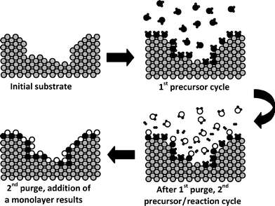 | ||
| Fig. 6 Schematic representation of a simplified model for the atomic layer deposition of a metal oxide using organometallic (●) and water (○) precursors. | ||
Atomic layer deposition has been used to modify a number of 3D surfaces including: aerogels of carbon,48–50silica,48,51,52alumina and germania;53polymer templates;54,55 anodic aluminum oxide membranes with high (>103) aspect ratios;56–58 200–400 nm diameter silica colloidal crystals;59,60 and mesoporous silica membranes.46,61 A wide range of ALD-derived films exist, including: (i) metals such as ruthenium,48tungsten,49,53copper,51 and palladium;57 (ii) oxides of tungsten, molybdenum,46titanium,46,54,55,59vanadium,46,62zirconium,52,56,58aluminum,58,63 and silicon;61 and (iii) nitrides of copper,51tungsten,64 and molybdenum.65 The application dictates the choice of substrate, composition of the coating, and the number of layers deposited; a range of morphologies can result.66 In addition to energy storage,53ALD has been used to fabricate materials for such other applications as single52,58,62 or multistep catalysis,49 photonics,54,55,59,60metallization of mesoporous solids,49 manufacturing electronic devices,67 sensing,54,57 accurate control of pore size for separations,61DNA translocation,63 creating templates and molds,54,64,65 and increased structural stability.68
The apparent simplicity of ALD masks underlying mechanistic complexity. The interaction between the precursor and the surface dictates the growth process and morphology of the film.46,48,51,56 Regardless of the ultimate composition that is desired, deposition of a “primer” layer of alumina49,52 or titania46 is often a prerequisite. Likewise, nucleation may require a few cycles to become steady state,49,53,57 and the nucleates may express in varied morphologies such as islands that coalesce,57 isolated crystallites53 or nanoparticles.48,50,53
Considering the underlying complexity of ALD, controlled deposition within 3D structures can only be accomplished if precursor–surface interactions are well-understood.67 Because the precursors are gas phase and the substrates have small openings and spaces, the path of the precursors can be modeled as Knudsen diffusion,51,61,62 which governs molecular paths limited by the size of container and not the surrounding medium. The interplay between Knudsen diffusion and cycle periodicity can also control where precursors land.56 Other factors that can limit the quality of internal coatings in 3D viaALD include the size and volatility of the precursors, especially when substrate voids become very small,48,51,56 and the thickness and composition of the substrate.48,51,63,64 While it is desirable to minimize cycle time in order to efficiently use often expensive precursors, an unoptimized duty cycle can lead to nonuniform films.48,51,64
2.4 Electrodeposition of polymers
Few techniques offer the flexibility inherent to electropolymerization when one wants to design electrically conductive 3D nanoarchitectures painted inside and out with ultrathin (10–100 nm thick) conformal polymer films.69 Potential- and current-controlled techniques are often used to fabricate polymer films on planar surfaces, particularly when electroactive films, such as polyaniline70 and polythiophene, are desired.71 Numerous examples focused on energy-storage applications exist in which an electroactive polymer is deposited on a planar electrode by electro-oxidizing the monomeric precursor in acidic aqueous solution.71–78 The thickness of such electroactive polymeric films is typically manipulated by monitoring electrochemical variables such as the coulombic charge that accrues during deposition.Molecular-level control remains challenging considering the chemical and physical heterogeneity of electrode surfaces, even those in 2D. Related work in the area of amperometric biosensor technology demonstrates that control of film thickness for ultrathin polymer coatings is gained by selecting deposition conditions in which the growing film is not electroactive.79–82 Such self-limiting methods deposit materials on the molecular length scale and result in a uniformly thick coating on all electrifiable interfaces until a critical thickness and electrical resistance is reached.
For arylamine monomers of interest in electrochemical capacitor systems, for example:
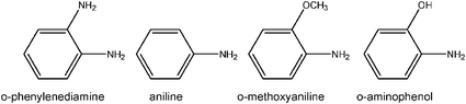
The first demonstration of self-limiting electropolymerization in a nanoscopic 3D electrode architecture established that aperiodic, mesoporous manganese dioxide (MnO2) ambigels are passivated by electro-oxidizing o-phenylenediamine at the oxide walls to form conformal, ultrathin (7–9 nm) coatings.69 Despite their nanoscopic dimensions, poly(o-phenylenediamine) (POPD) films are pinhole-free and prevent the electrochemical dissolution of MnO2 in aqueous acid, while also permitting ion-gated proton insertion into the underlying porous MnO2electrode nanoarchitecture.69 In a dry, as-deposited state, the ultrathin POPD serves as an electronically insulating coating on the nanostructured oxide, as determined by conductive probe AFM.91
Likewise, ultrathin arylamine polymers can be conformally deposited onto the walls of aperiodic mesoporous/macroporous carbon aerogel and nanofoam electrodes (see Fig. 7(a)), while preserving the through-connected pore structure of the carbon nanoarchitecture (Fig. 7(b)). For EC applications, the redox reactions of the polymer in acidic electrolytes increase the charge-storage capacity of the resulting hybrid polymer–carbon nanoarchitecture by factors of two or greater, as shown in Fig. 7(c).92,93
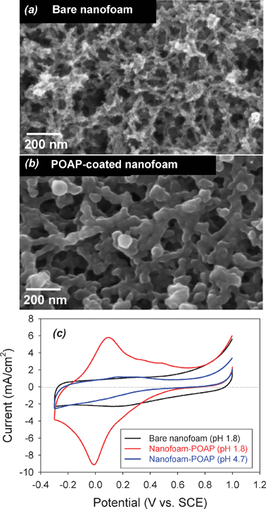 | ||
| Fig. 7 Scanning electron micrographs for (a) bare and (b) carbon nanofoam paper coated with poly(o-aminophenol), POAP; and (c) cyclic voltammetry at 2 mV s−1 for the bare and POAP-coated carbon nanofoams in aqueous electrolytes of different pH. | ||
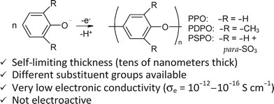 | ||
| Fig. 8 The electroreaction whereby ultrathin conformal polymer films are synthesized viaoxidation of phenolate monomers onto ultraporous electrically conductive nanoarchitectures and some of the attributes of the resulting polymer. | ||
For PPO-coated MnO2 ambigel electrodes, the polymer does not impede Li-ion insertion into the underlying MnO2 cathode100—a critical factor for the subsequent assembly of energy-storage devices comprising 3D-interpenetrated electrode nanoarchitectures.7 As-deposited PPO films are permeable to bis(2,2′,2″-terpyridine)cobalt(II) molecular redox probes, but shut off molecular transport (as well as direct electron transport at the polymer–electrolyte boundary) after the oligomeric coating is thermally annealed under vacuum at 150 °C. This ability to permeate molecules and ions into as-deposited films is an important feature that allows one to modify the film or underlying electrode before using thermal annealing to seal in desired molecular or ionic reactants, as we discuss below.
The dielectric strength of ultrathin, electropolymerized PPO (1.7 × 10⁶ V cm−1) matches that of PPO films 102–103× thicker, indicating that the electrodeposited PPO films are high-quality dielectrics as well as promising ultrathin electrolyte/separators for solid-state ionic devices. This dielectric strength is sufficiently high to withstand those that would develop in a nanoscopic 3D battery, even one with Li chemistry where >3 V can be dropped across 10 nm.
The ultrathin PPO coating can be transformed into an ionically conducting separator (with 7 × 10⁻¹⁰ S cm−1 at room temperature) simply by soaking in nonaqueous lithium electrolytes prior to thermally annealing the polymer.99 Such ionic conductivities are low relative to conventional polymer electrolytes,101,102 however at tens of nanometers separation between anode and cathode in the 3D battery design, the effective Li-ion transport rates will be sufficient for operation at high charge–discharge rates. For example, with a 10-nm separation and 10−9 S cm−1, the equivalent resistance between the electrodes would be 10 Ω.
The ionic conductivity of PPO is significantly enhanced by incorporating ionic or ionizable functionalities into the polymer structure. A 3:1 co-polymer of 2,6-dimethylphenol (DMP) and 4-hydroxybenzene sulfonic acid (sodium salt, HBS) achieves 102 higher Li-ion conductivity (4 × 10⁻⁸ S cm−1) without compromising the conformal nature of the nanoscopic coating (compare Fig. 9(c) for the co-polymer to Fig. 9(b) showing the pure dielectric response and conformal coating characteristic of poly(2,6-dimethyl-1,4-phenylene oxide), PDPO).103 In contrast, nonuniform polymer coatings are produced by electropolymerizing HBS on ITO to form poly(4-sulfonic acid-1,2-phenylene oxide), PSPO (Fig. 9(a)). These results demonstrate that the homogeneity of ultrathin polymer films varies as a function of multiple parameters, such as polymer solubility in the reaction solvent and the electron-transfer kinetics specific to each monomer molecule at a particular electrode material.
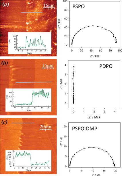 | ||
| Fig. 9 (Left) AFM images and line-trace profiles (inset), and (right) solid-state impedance of electrodeposited (a) PSPO, (b) PDPO and (c) PSPO:DMP. The horizontal lines in the AFM images indicate the position of the line trace. Two-point probe impedance was obtained at ITO||polymer||Ga–In with a 50 mVac voltage and 0 Vdc bias from 1 MHz to 100 Hz. (Adapted from ref. 103 and reproduced with permission; copyright 2005, Electrochemical Society.) | ||
Poly(phenylene oxide) has been functionalized with boronic acid under self-limiting conditions on a planar Au electrode in order to detect simple sugars as a biosensor,104 but the ionic conductivity of this co-polymer has not been reported. Ionic function can also be introduced into pre-formed films by chemical grafting, but the modification conditions must be sufficiently mild not to damage such ultrathin films.
Secondly, many electro-oxidizable monomers, including the ever-important phenol series, are unstable in the presence of oxygen, and should be stored and reacted under inert atmospheres. It is common to observe color changes in the monomer solution as oligomers with conjugated unsaturated bonds form,98 although best practices dictate that colloids should be absent in the reaction mixture prior to use. Furthermore, electroactive monomer solutions are potentially sensitive to photoinitiation, and should be prepared in dark bottles in order to avoid forming colloids that would hinder the uniform coating of heterogeneous pore structures. Finally, electro-oxidative reaction schemes are largely incompatible with all but the most noble metals, making conductive glasses, oxides and carbons preferred as current-collecting substrates under oxidizing conditions.
Thirdly, the >100-fold surface area difference between planar electrodes used in typical electrochemical measurements and the high surface areas customary for nanoarchitectures requires an awareness of monomer concentration and cycle number in order to achieve comparable levels of passivation. Even a 1.5-μm thick MnO2 nanoarchitecture synthesized on an ITO current collector requires more cycles at slower sweep rates to achieve passivation (Fig. 10) and yet when passivated retains a capacitive current–voltage response indicative of the dielectric being electrogenerated, but expressed as a high-surface-area dielectric.99,100
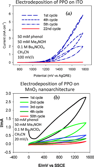 | ||
| Fig. 10 Potential sweep deposition of poly(phenylene oxide), PPO, films on (a) ITO and (b) ITO-supported MnO2 ambigel electrodes. (Reproduced with permission: (a) ref. 99; copyright 2004, American Chemical Society.) | ||
2.5 Electrodeposition of metals and compounds
A strategy that reshaped the nature of on-chip metallization in the microelectronics industry might be adaptable to the controlled deposition of conformal films within 3D structures. In IBM’s award-winning Damascene process, metallic Cu preferentially electrodeposits into trenches and other subsurface features on microelectronic wafers, filling them without overcoating the upper surface of the wafer.108 Shifting the primary site of Cu electrodeposition from the open, flooded surface to the interior features etched into the wafer is achieved by adding to the plating bath reagents that suppress the kinetics of Cu deposition. These additives initially contact the upper surface of the wafer, lowering deposition there, while the subsurface features being less accessible to the kinetics-suppressing additives (because of hindered diffusive mass transport) experience higher rates of Cu deposition and fill with the electrogenerated metal.108,109 As tailored to modification of 3D electrode structures, the goal would be to electrodeposit conformal films to a desired thickness at the internal surfaces without filling the void volume.An electrochemically controlled variant on atomic layer deposition (formerly known as EC-ALE) couples the monolayer finesse of ALD, but by using cycles of precursors in liquid electrolytes, while introducing the discrimination of potential control in order to create ultrathin layers of metals and semiconductor compounds at electrode surfaces.110 The react/purge/react cycles characteristic of gas-phase ALD can be adapted for the liquid electrolytes necessary for the electrochemical analog by the use of automated flow cells, including microfluidic control. Although most of the reports in this area focus on the II–VI and III–V chalcogenide-based semiconductors, these materials are of energy relevance for photovoltaics and thermoelectric materials. Ultrathin metal films have also been prepared by ALD electrodeposition (EC-ALD),110,111 including Ru.112
2.6 Electroless deposition of mixed-conducting metal oxides
Transition metal oxides dominate the landscape of materials for electrical energy storage in secondary (i.e., rechargeable) batteries. More recently, the use of mixed-conducting metal oxides has been extended to electrochemical capacitors (ECs), where the redox reactions of the metal oxide (i.e., pseudocapacitance) can increase the energy density of ECs relative to high-surface-area carbons, which store charge primarily as double-layer capacitance. One of the most extensively studied metal oxides for use in electrochemical capacitors is hydrous ruthenium oxide (RuOxHy or RuO2·xH2O) with a pseudocapacitance of 720 F g−1,113,114 a mass-normalized value all the more impressive because the capacitive storage of ionic charge at even high-surface-area carbons is typically on the order of 100–200 F g−1.Hydrous ruthenium oxide offers several attractive properties for use as an electrode material in energy-storage applications, including reasonable electronic conductivity (1 S cm−1),115proton conductivity comparable to Nafion™ (at 1 mS cm−1),116 high pseudocapacitance,113,117 and chemical stability,118 but its prohibitive cost ($280 USD/troy ounce ($9.00 USD/g), June 2008119) has motivated the search for alternative materials. Under study for use in electrochemical capacitors are other transition metal oxides that exhibit pseudocapacitance, such as various phases and polymorphs of manganese dioxide,120–128iron oxide,129–132nickel oxide,133–136cobalt oxide,137–141 and tin oxide.142–147 Of this series, manganese and iron oxides are both environmentally benign and inexpensive. However, none of the reported capacitance values for these materials yet approach the values of RuO2 pseudocapacitance as seen in Fig. 11.148 It should also be noted that polymer-based ECs cannot meet the performance of oxides.
![Comparison of the pseudocapacitance values reported in the literature for various materials under study as electrochemical capacitor electrodes. PFDT: poly[3-(4-difluorophenylthiophene)]; MPFPT: poly[3-(3,4-difluorophenylthiophene)]; DAAQ: diaminoanthraquinone; PEDT: 3,4-poly(ethylenedioxythiophene); PPy: polypyrrole; AC: activated carbon; PAPPA: poly[3-(4-aminophenyl)propionic acid]; CB: carbon black; CNT: carbon nanotube. (Ref. 148; copyright 2008, Electrochemical Society.)](/image/article/2009/CS/b801151f/b801151f-f11.gif) | ||
| Fig. 11 Comparison of the pseudocapacitance values reported in the literature for various materials under study as electrochemical capacitor electrodes. PFDT: poly[3-(4-difluorophenylthiophene)]; MPFPT: poly[3-(3,4-difluorophenylthiophene)]; DAAQ: diaminoanthraquinone; PEDT: 3,4-poly(ethylenedioxythiophene); PPy: polypyrrole; AC: activated carbon; PAPPA: poly[3-(4-aminophenyl)propionic acid]; CB: carbon black; CNT: carbon nanotube. (Ref. 148; copyright 2008, Electrochemical Society.) | ||
One major challenge for both sol–gel and hydrothermal methods is that the resulting metal oxides are not highly conductive and must be mixed with a more electronically conductive component (e.g., carbon powder) as well as a binder (e.g., poly(tetrafluoroethylene), PTFE) in order to be formulated into an electrode structure. Powder composite fabrication is typically a multistep, time-intensive process that not only adds additional, electro-inactive mass, but also may result in agglomeration of the metal oxide particles, surface passivation of the metal oxide by the additives, and thick metal oxide deposits, all of which reduce effective utilization of the electrode structure.121,129,137,147
Depositing the metal oxide directly onto a substrate of high electronic conductivity eliminates the need for conductive additives with concomitant binders. Electrodeposition of oxides is widely used to modify both planar and non-planar substrates, and offers some control over deposition rate, film thickness, composition, microstructure, and morphology.117,118 Electroless deposition is a relatively inexpensive and simple method for producing conformal metal oxide films on a variety of complex substrates (e.g., spherical particles, planar surfaces, porous carbon nanofoams, and nanotubes). The thickness of electrolessly deposited films depends on several experimental factors including reaction time, temperature, and pH.120,124,125 For example, Wang et al. reported the electroless deposition of Fe3O4 crystallites of unspecified size onto the surfaces of a carbon black powder (with a surface area of 220 m2 g−1). The oxide–carbon hybrid yielded a specific capacitance of 510 F g−1 (normalized to the mass of oxide) as compared to a specific capacitance of 30 F g−1 for 34 m2 g−1 Fe3O4 particles (14–29 nm) that were physically mixed with carbon black powder.129
Although simply soaking an oxidizable 3D structure in aqueous permanganate solutions is an attractive and straightforward approach, careful control of the permanganate reduction reaction is required to achieve nanoscale MnO2 deposits throughout an electrode nanoarchitecture, as well as to inhibit the formation of thick MnO2 coatings on the boundary of the porous electrode. Thus, in analogy to the polymeric systems, the key to this approach is to exploit conditions that promote self-limiting deposition as depicted in Fig. 5.
The use of electroless techniques to produce nanoscopic and conformal metal oxide coatings or deposits within ultraporous 3D architectures provides several advantages over conventional synthetic techniques, including retaining the high specific surface area of the 3D porous substrate, maintaining electrolyte access to the interior bulk of the electrode through the interconnected pore network, and achieving higher mass loadings in a given volume.120,125,126 In addition, the conformal nature of the ultrathin deposits reduces the limitations introduced from the electrical resistivity of the metal oxide,120,123,125 with the underlying electrode nanoarchitecture acting as a massively parallel 3D current collector. Maintaining the nanoscopic nature of the oxide coating should optimize the pseudocapacitance of the resulting hybrid electrode. For example, manganese oxide has been deposited on monolithic carbon nanofoam electrodes to produce nanoscopic MnO2 deposits within the tortuous interior of macroscopically thick porous carbon nanofoam substrates.120,152
Self-limiting deposition is favored at neutral pH and produces conformal, nanoscopic MnO2 deposits throughout the macroscopic thickness (100–200 μm) of the carbon nanofoam electrodes, while maintaining the through-connected pore network of the native carbon nanofoam.120 In contrast, a macroscopically thick MnO2 crust is produced on the exterior boundaries of carbon nanofoam under acidic conditions,120 due to the autocatalytic deposition of MnO2 at low pH.153,154
As shown in the transmission electron micrographs (TEM) in Fig. 12, the nanoscale oxide electrolessly deposits as the lamellar MnO2 polymorph, birnessite, but the morphologies vary as a function of deposition pH. Ribbons and rods permeate the carbon nanofoam under neutral deposition conditions (Fig. 12(a)), whereas agglomerated nanoparticles of birnessite-type MnO2 are produced under acidic conditions (Fig. 12(b)). The elemental scanning TEM maps for neutral-deposited MnO2 in Fig. 12(c) provide evidence for additional homogeneously distributed MnO2 within the carbon nanofoam. Such conformal deposition throughout the interior of the carbon nanofoam under neutral conditions in this study produced an area-normalized capacitance of 1.5 F cm−2, which is orders of magnitude higher than the areal capacitance typically reported for other C–MnO2 composites at 10–50 mF cm−2.120 This level of footprint-normalized energy storage should satisfy the power requirements of smart dust and related microdevices with per day requirements of 1 J mm−2.12,13
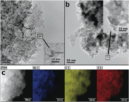 | ||
| Fig. 12 Transmission electron micrographs of (a) neutral-deposited and (b) acid-deposited MnO2 on carbon nanofoam with (c) scanning TEM elemental map of the neutral-deposited sample. | ||
We have investigated the subambient thermal deposition of RuO2 directly nucleated at electropolymerized nanoscale (21 ± 2 nm) PPO films deposited on planar ITO and polymer-coated mesoporous MnO2 substrates. Transmission electron microscopy demonstrates that this protocol generates ∼2-nm RuO2 particles that adhere to the polymer and deposit as a self-wired path of conductive RuO2. Solid-state electrical measurements of RuO2 deposited on PPO-coated ITO in a planar configuration demonstrate that nanoscopic RuO2 can be deposited by this protocol without electrically shorting through the ultrathin polymer film to the ITO substrate.156,157
2.7 Specific adsorption of metal nanoparticles
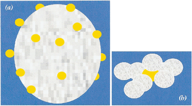
Multifunctional nanoarchitectures may be created in some cases by incorporating colloidal metal nanoparticles onto the 3D interfaces of porous scaffolds. Host surfaces can be modified with chemical and biological158 moieties that specifically bind preformed nanoparticles uniformly distributed throughout a supporting material. Gold nanoparticles can be tethered to carbon nanotubes at acidic surface sites,159thiol linkages,160 and via attractive electrostatic interactions with adsorbed polyelectrolyte layers.161 Commercially available Vulcan carbons are high-surface-area supports that covalently anchor metal nanoparticles, including the Pt and PtRu electrocatalysts used in fuel cells,162,163 to adventitious thiophenyl functionalities at the carbon interface.164Vulcan carbon powders are usually engineered into monolithic electrode structures by homogeneously incorporating ionomeric additives (for proton conduction throughout the electrode structure) and polymer binders, but these components may decrease overall accessibility to the internal carbon surface area. Vulcan carbon premodified with 2-nm Pt colloids can instead be ‘nanoglued’ into an electrode structure by infiltrating the intergranular voids with silica sol that subsequently gels around the carbon agglomerates, creating monolithic solids that are electronically conductive. The resulting Pt/C-silica architecture, weight saturated at ∼10 wt% Pt, increases the activity of methanol oxidation per gram of Pt by factors of at least 10 relative to conventional electrocatalysts.3 The silica network maintains facile fluid transport of methanol molecules throughout the 3D nanocomposite. Because the Pt nanoparticles are sited on the carbon walls and not in the carbon micropores (pores sized <2 nm), fuel readily finds catalyst surface for reaction.
Sulfur-based receptor sites readily bind precious metals, and our group has developed a strategy that incorporates thiophenyl moieties at the walls of carbon aerogels.165Thiophene-based species are covalently grafted to the surface of phenolic polymer gels via an acid-catalyzed addition reaction, and survive pyrolysis such that they mimic the thiophenyl functionality of Vulcan carbon and readily bind preformed metal nanoparticles from aqueous sols. As seen in Fig. 13, 2-nm Pt colloids are not adsorbed by standard carbon aerogel, while the 0.5 wt% thiophenylated carbon aerogel exhaustively depletes the Pt colloidal sol.
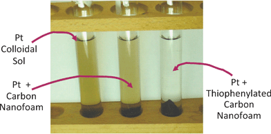 | ||
| Fig. 13 Photograph illustrating that decoloration of Pt sol arising from adsorption of Pt nanoparticles occurs only at C∼S (thiophenylated carbon) nanofoam. (Left) Pt sol; (center) Pt sol and ground carbon nanofoam (right) Pt sol and ground C∼S nanofoam. (Adapted from ref. 165; copyright 2004, Elsevier B.V.) | ||
Designing the anchor site at the walls of the carbon nanoarchitecture allows nearly all of the surface atoms of the S-sited Pt nanoparticles to bind a small molecular probe (CO)—86% of the Pt surface atoms adsorb the probe molecule.165 This enhanced surface expression of Pt is critical for lowering the amount of Pt in a fuel-cell electrode while retaining the molecular turnover rates necessary for high performance. Carbon interfaces do not necessarily require sulfur modification to adhere metallic nanoparticles; nitrogen heteroatoms appear to serve as electron-rich sites for nucleation and growth of catalyst nanoparticles.166,167 Direct methanol fuel cell (DMFC) PtRu catalysts have been deposited onto carbon cryogels by chemically reducing Pt and Ru salts in excess borohydride solution and by electrochemically reducing the same precursor salts onto carbon–Nafion™ composites.168 Supercritical fluid impregnation of carbon aerogels with thermally labile platinum complexes followed by decomposing the Pt-precursor in N2 (g) at 300–1000 °C led to ≤40 wt% of <10-nm Pt nanoparticles supported on the carbon nanoarchitecture.169
3. Challenges for characterization of multifunctional 3D nanoarchitectures
In order to develop clear correlations between the structure of an architecture and its properties, it is critical to determine the nature of the solid and pore networks and then establish the nature of the multifunctionality of the edifice, specifically its physical, electrical, electrochemical, mechanical, thermal, magnetic, and optical properties. It should then be no surprise that wide-ranging physicochemical characterization is essential to understand aperiodic materials and optimize the properties and performance of these systems for various applications (i.e., catalysis, energy storage, photovoltaics).The characterization of 3D architectures presents particular challenges beyond those present for planar systems with similar components. Many of these challenges arise from overlap with issues affecting characterization of nanoscale particles170–173 and porous materials.174,175 Some of the specific challenges encountered for the characterization of 3D nanoarchitectures are: (i) the dominant contribution of the surface driven by surface-to-volume ratios that approach 1 × 106 cm−1; (ii) the related fact that the bulk of the architecture is sub-surface, with buried interfaces; (iii) the often disordered nature of the nanostructured solid phase; (iv) interparticle interactions (e.g., electrical, magnetic); (v) the difficulty of characterizing multicomponent systems; and (vi) the aperiodic pore structure of materials such as aerogels.
We find that the following in-lab suite of materials science analyses provide a reasonable understanding of the character of a given aerogel or modified aerogel, thereby allowing us to optimize synthetic and fabrication strategies. For example: simultaneous differential scanning calorimetry and thermogravimetric analysis (as a function of heating rate and atmosphere) guide our thermal treatments of both oxides and polymer coatings. X-Ray diffraction analysis of the supercritically dried aerogel (which is usually amorphous) and the thermally processed aerogels and ambigels give us an indication of the “bulk” structure of the solid. Physisorptive analyses provide surface area, pore volume (the fraction of the aerogel volume that can potentially be filled by a second nanoscopic phase) and the distribution of pore sizes.
Premier samples can be further characterized by field-emission scanning electron microscopy, transmission electron microscopy, small-angle neutron scattering (to verify morphology and feature size), X-ray photoelectron spectroscopy (to verify the chemical speciation of the material; on occasion X-ray absorption spectroscopy at a synchrotron is useful), and vibrational spectroscopy, such as Raman microprobe analysis (to characterize the metal–oxygen vibrational modes) and FTIR (to characterize the nature of ultrathin polymers). Solid-state nuclear magnetic resonance is also proving to be an important means to characterize local structure and the electronic state of insertion battery materials.176
Impedance spectroscopy (as a function of processing conditions, e.g., heating rate and atmosphere) provides insight into the conduction mechanisms of the transition metal oxides—these solids expressed as aerogels (i.e., with negligible bulk and dominated by the networked interface) are typically mixed conductors of electrons and protons/cations. Impedance spectroscopy is also a primary method to establish the quality and character of the fully assembled nanobattery. Electroanalytical surveys of these high-surface-area solids (as-made and after various modifications) are performed by pressing sub-milligram quantities of the aerogel onto the surface of a “sticky carbon,” which is a composite of a high purity carbon and wax to obtain quantitative, high quality data on their intercalation and charge-storage characteristics.177,178
By determining the specific capacitance for the various aerogels (arising from either electron/proton or electron/Li+ charge storage) we have a solid predictor of the best intercalating electrode materials. For characterization of Li-ion intercalation into the various insertion oxide aerogels (both before and after coating with a separator layer), one can switch to a less-swelling carbon–beeswax sticky carbon to establish responses in traditional nonaqueous electrolytes containing lithium salts.177–179
3.1 Planar versus 3D structures
En route to the design, characterization, and ultimate utilization of multifunctional 3D nanoarchitectures, important fundamental information on physicochemical structure and electrical properties can be derived by examining the individual architectural components as ultrathin modifying layers on rough 2D substrates (such as ITO for oxide nanoarchitectures; glassy carbon for carbon architectures). With 2D substrates one can bring to bear the standard analytical tools of surface science and electrochemical science.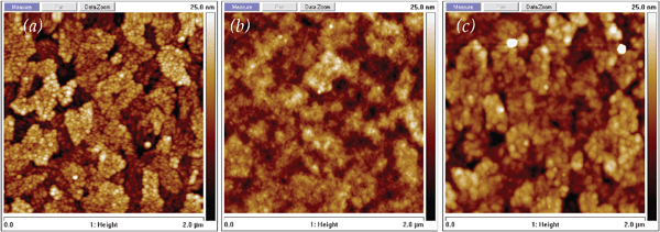 | ||
| Fig. 14 Atomic force micrographs for (a) clean ITO, (b) POMA-coated ITO via voltammetric (potential sweep) deposition, and (c) POMA-coated ITO via potentiostatic deposition. | ||
Although the platelet structure of the underlying ITO substrate (Fig. 14(a)) is still visible after film deposition, these images demonstrate that surface morphology and film thickness are functions of the deposition process, with finely featured, 18-nm POMA films produced by voltammetric cycling (Fig. 14(b)), while potentiostatic deposition yields thinner (7 nm) but more particulate coatings (Fig. 14(c)).180 Either surface morphology, however, differs significantly from those previously reported by Patil et al.181,182 and Vera et al.,183 who examined POMA films deposited from acidic solutions with pH values less than 6, conditions that are more typical for electrodepositing conventional conducting polymer films. Those POMA films were not self-limiting and yielded highly granular or fibular morphologies with thickness approaching several micrometers.
Structural characterization of conventional POMA films has also been reported using specular-reflectance infrared spectroscopy.184 Two characteristic bands at 1587 cm−1 and 1510 cm−1 are observed and assigned to quinoidal (Q-band) and benzene-like (B-band) functionalities, respectively. We observe similar features for ultrathin POMA on ITO (Fig. 15). Our data suggest that the as-deposited, self-limiting POMA film contains comparable contributions from quinoid-like and benzene-like units, consistent with the following structure:
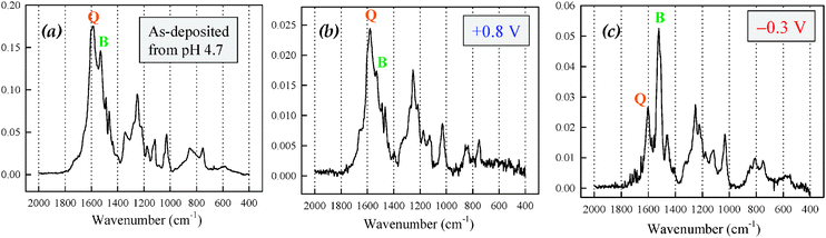 | ||
| Fig. 15 FTIR spectra of POMA films electrodeposited on ITO-coated glass: (a) as-deposited and after potentiostatting in 0.1 M H2SO4 to (b) +0.8 V vs.Ag/AgCl and (c) −0.3 V vs.Ag/AgCl. | ||
The ratio of the intensity of these two functionalities is unchanged after immersion in acidic solution (0.1 M H2SO4) for 5 min at +0.8 V (vs.Ag/AgCl). Upon poising the electrode potential for 5 min at −0.3 V, the B:Q ratio increases significantly, indicating electrochemical formation of the benzene-like functionality by reduction of the quinoidal functionality (Fig. 15).72 Our group is currently conducting additional structural characterizations using other surface-sensitive techniques such as X-ray photoelectron spectroscopy to develop a more fundamental understanding of the chemical structure of the ultrathin electrodeposited polymer films.
As an example of 2D two-component electrical analysis, we have preliminary evidence that we can control the rate of deposition and size of a second ion-insertion electrode—both factors are critical for controlled infusion of a Li-insertion anode into the remaining free volume in a PPO-coated nanoarchitecture. Adapting our previous deposition of nanoscopic RuO2 from alkane solutions of RuO4 at subambient temperatures,155 we find that we can deposit 2-nm spheres of disordered RuO2 on PDPO (a PPO relative, poly(dimethylphenylene oxide)) electrodeposited on ITO and on PPO that was electrodeposited on a cathode nanoarchitecture of ITO||MnO2 birnessite ambigel. The ruthenia nanoparticles appear to self-wire, which will be an important way to ensure that internal deposits within the nanoarchitecture are interconnected (Fig. 16).
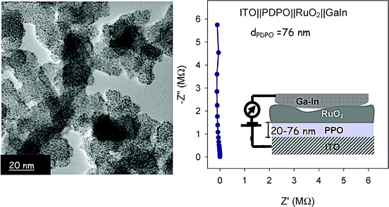 | ||
| Fig. 16 Transmission electron micrograph showing nanospheres of RuO2 deposited onto PPO-coated ITO||MnO2 ambigel; and the AC impedance of ITO||PDPO||RuO2||GaIn. Comparable responses were obtained for three out of five deposition attempts; the other two samples shorted. | ||
3.2 Characterization of disorder and distributed states
One of the broad characterizational challenges of 3D nanoarchitectures is to physically, structurally, and chemically discern the disordered nature of the nanoscopic solid phase. The role of disorder, particularly at surfaces, is amplified for nanoscale materials, which is an important fact of life for energy storage and conversion because the electrified interface mediates all energy-relevant reactions. Numerous materials characterization methods such as X-ray diffraction, electron diffraction, Raman and infrared spectroscopy, and extended X-ray absorption fine structure provide information on order/disorder at various size scales, ranging from >3 nm in the case of X-ray diffraction, down to a few bond lengths in the case of vibrational spectroscopy and EXAFS. Missing from the characterizational arsenal is information on the most relevant length scale for nanomaterials and electrochemical interphases in power sources: 1–3 nm. Structural information in this size regime can be provided by pair distribution functional analysis of synchrotron-derived X-ray or neutron diffraction,189–192 but this technique is only slowly being adopted for characterization of nanoscale features and materials.Three-dimensional multifunctional nanoarchitectures are an ensemble of buried interfaces. An additional challenge is to characterize the structural, energetic, and spatial distributions within the 3D architecture rather than an average structure or state that is distributed throughout the architecture. The analytical tools to-date average the information in these systems, whether surface-sensitive (measuring information at the boundary of the architecture) or penetrating such as X-ray absorption or Raman spectroscopy. Information with lateral and depth resolution of the physicochemical nature of multifunctional nanoarchitectures is an area requiring new tools such as recent work using scanning transmission electron microscopy to determine three-dimensional size and shape of structures within a tin/silicon quantum dot system170 and our tricontinuous co-location of MnO2 nanoarchitectures overcoated with PPO and nanoscopic RuO2.157
3.3 Characterization of interparticle interactions
The interconnectivity and physicochemical interactivity between the individual nanoparticulate building blocks comprising the network of the 3D architecture establishes the structure–property relationships of the edifice. Understanding such interactions represents another characterizational challenge; to date very little work has been performed to decipher interparticle interactions within 3D nanoarchitectures. The interaction of dispersed colloids and nanoparticles is unlikely to be relevant as a model for interactions in covalently networked nanoarchitectures in that particle–particle interactions in the network are not strictly determined by surface-to-surface interactions. The physical landscape has three aspects: (i) a core of 1D connectivity arising from the covalent self-wiring of the colloidal sol particles during gelation; (ii) the concave divots that exist between the bonded (often globular) particles; and (iii) the reticulated, interconnected surface skin of the network.Our previous work has highlighted the importance of interparticle interactions on magnetic, catalytic, mechanical, and electrical properties. The individual nanoparticles comprising an iron oxide aerogel were shown to be magnetically interactive for phase-pure forms, such as γ-Fe2O3, whereas for mixed-phase Fe3O4/γ-Fe2O3 aerogels, magnetic coupling between the individual nanoparticles is frustrated.193 The interaction of ∼6-nm Au with multiple ∼12-nm TiO2 particles (Fig. 17(b)) played a specific role in the catalytic activity observed of TiO2–Au aerogels for the room-temperature oxidation of CO.194
 | ||
| Fig. 17 Contrasting old vs. new bifunctional catalysts: (a) standard “flea on a boulder” catalyst in which a metal or metal oxide catalytic flea, as represented by yellow dots, is impregnated/deposited onto an active support that is typically an order of magnitude larger in size; and (b) an architectural design for bifunctional neighbors in which the metal catalyst at ∼5 nm is comparably sized to its active oxide support at ∼12 nm and in which multiple points of metal–oxide contact exist. | ||
Silica monolithic samples prepared without aging in the mother-liquor sol, supercritically dried, and then densified by heat treatment showed differences in pore structure and substantially different mechanical properties than a standard silica aerogel after thermal densification.195 Although the former materials had a lower Young’s modulus than the latter, they were more fracture resistant, which was attributed to thicker regions of connectivity (“necking”) between particles. Interconnectivity between particles was also shown to strongly affect the electrical properties of MnO2 nanoarchitectures, as displayed by sensitivity to humidity.196 The monolithic nanoarchitecture was ten-fold less resistive than films prepared from monolithic particulates in which physical junctions were introduced between particulates.
3.4 Characterization of disordered pore structure
An accurate characterization of the architectural pore structure is critical, because pores (i.e., void space) represent the dominant volume fraction (typically more than 75%), and often determine the properties and performance of a multifunctional nanoarchitecture. For example, the tortuosity of the pore network affects the transport of solvated lithium ions within the pores of mesoporous V2O5 with ordered macropores.197Pore structure also influences fluid transport within the architecture, which is critical for such applications as electrocatalysis, heterogeneous catalysis, sensing, and modifying the interior of the architecture to introduce new functionality.A particular challenge arises with pore structures that are aperiodic and polydisperse, as in the case of sol–gel-derived nanoarchitectures such as xerogels, aerogels, and related materials. The predominant methods to analyze pore structure are nitrogen physisorption and mercury porosimetry. Nitrogen physisorption has particular challenges applied to disordered pore networks.174 Reichenauer and Scherer have discussed how the nanoscopic networks in underdense silica aerogels can undergo compression by forces induced by the quadrupolar moment of molecular nitrogen.198 Compressing the walls affects the pore structure at 77 K (as the measurement is performed in liquid nitrogen) and can lead to an assessment of the pore-size distribution that does not reflect the nature of the pore structure at room temperature.
Porosimetry also allows the effect of an added component or internal coating to be gauged. Comparing the pore size distribution before and after electrodepositing a POMA film at the walls of a carbon aerogel clearly shows the smooth filling of the polymer into the pore volume, Fig. 18.199
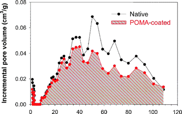 | ||
| Fig. 18 Pore-size distribution plots derived from N2-adsorption isotherms for a carbon nanofoam before (native) and after electrodeposition of an ultrathin poly(o-methoxyaniline), POMA, coating. | ||
3.5 Characterization of multicomponent 3D systems
If the free volume in two-component nanoarchitectures remains sufficiently large and interconnected (as in ultrathin polymers coated on mesoporous, nanostructured, high surface area MnO269,100 or carbon nanoarchitectures92), modification to form tricontinuous three-component architectures can be undertaken. The characterization of triphasic, interpenetrating, buried interfaces provides additional challenges beyond single-component systems, because the coverage, distribution, and properties of the individual components within the 3D architecture need to be determined. Standard methods suitable for planar systems can fall short when applied to 3D architectures.Electron microscopy has been a particularly useful tool for the characterization of 3D nanoarchitectures.200Transmission electron microscopy of a tricontinuous, three-phase composite of MnO2||PPO||RuO2, presented in Fig. 19, provided otherwise unobtainable information about both the nature of the polymer and RuO2 deposits and their interface.156,157 The lattice fringes of the birnessite MnO2 domains, observed for uncoated samples,201 were absent for the polymer-coated samples, indicating that the polymer electrodeposits within the MnOx nanoarchitecture and does so as an ultrathin layer. In addition, the TEM analysis showed that the deposited RuO2 forms within the nanoarchitecture, remains nanoscopic, and self-aggregates to wire its way throughout the nanoarchitecture. Depth-of-focus imaging confirmed that the 2-nm RuO2 particles reside on the uppermost surface of the ultrathin polymer.
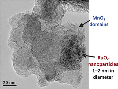 | ||
| Fig. 19 Transmission electron micrograph of MnO2||PPO nanoarchitecture after internal deposition of nanoscopic RuO2via the subambient thermal decomposition of RuO4. | ||
Many powerful and useful characterization methods still result in predominantly 2D resolved analysis. Expanding into 3D using depth profiling and tomographic analysis will be crucial for characterizing these complex architectures.202 With recent advances in 3D TEM, one can now obtain information on the size-distribution and connectivity of nanoscale pore networks in complex nanocomposites and determine the spatial distributions of incorporated nanoparticles, to a resolution of (1.5 mm)3.
4. Designing multifunctional architectures for 3D electrochemical power
Power is a rate-critical phenomenon: events per second sustain the application. Increasing the number of events per second requires ensuring facile transport of reactants (electrons, ions, molecules) to the structured electrode and rapid electron-transfer kinetics at the electrode. As we discuss in this section, an architectural perspective and a blend of order with disorder impart a formalism that can improve the performance of electrochemical power devices as one more optimally blends all of the necessary reaction and transport rates.4.1 Balancing diverse transport requirements: ion vs. electron vs. fluid
Just as we expect electrons to be wired to where they are needed, optimal power performance is most effective when the transport paths through which all the charges and molecules move are integrally designed into the power-generating architecture. When designing an energy functional nanoarchitecture, the charge transport paths can be self-wired and the width of the internal plumbing can be established courtesy of sol–gel chemistry and processing wet gels under conditions of low-to-minimal surface tension.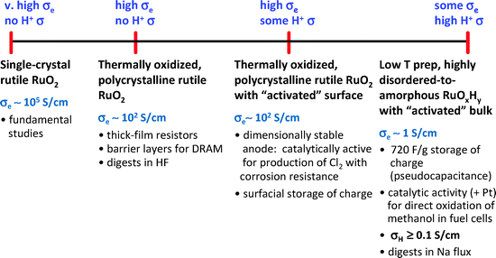 | ||
| Fig. 20 Ruthenium oxides—an example of the spectrum of properties for one metal oxide as disorder creeps into order. (Adapted from ref. 203; copyright 2003, American Chemical Society.) | ||
Polycrystalline RuO2 exhibits reduced electronic conductivity (ca 102 S cm−1), but ionic transport is only facilitated if the oxide surface is first thermally or electrochemically activated to incorporate defects preferentially at interfaces.212 It has only been recently recognized that hydrous ruthenia is a natural nanocomposite with a nanoscopic rutile crystalline network (with 1–2 nm crystallites in RuO2·xH2O with x∼2) interpenetrated by a disordered hydrous structure.190 This inorganic analog to block co-polymers facilitates the motion and storage of protons in aqueous acidic electrolytes while retaining metallic electron conductivity, thereby explaining the high level of pseudocapacitance exhibited by this oxide.113–115,149 The fortuitous multifunctional structure inherent to hydrous ruthenia illustrates an important lesson for designing new active materials for pseudocapacitive ECs: one should create a composite where the ion transport phase is nanoscopic and fully underwired by a high electron-conductive support.
The balancing act between ionic and electronic transport in RuO2 is further illustrated by the Li-ion insertion behavior of RuO2nanoparticles (nano-RuO2) prepared by subambient thermal decomposition of RuO4.179 As prepared, nano-RuO2 is anhydrous but structurally disordered, yielding diffuse electron diffraction rings. When examining Li-ion insertion over potential ranges of relevance for use as a cathode (1.5–4 V), as-prepared nano-RuO2 yields a specific capacity of ∼200 mA h g−1 (Fig. 21). Heating the as-prepared material at 200 °C generates a highly crystalline, but still nanoscopic RuO2 phase, and consequently reduces the Li-ion capacity to ∼100 mA h g−1.
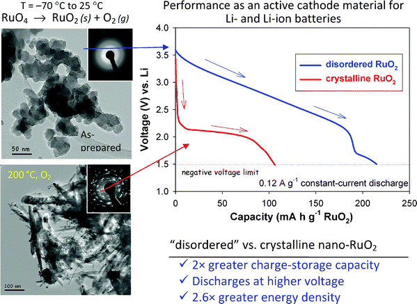 | ||
| Fig. 21 Subambient thermal decomposition of RuO4 in a hydrocarbon solvent yields nanoscopic RuO2 in an anhydrous, but disordered form (upper micrograph and electron diffraction pattern). This form of the nanomaterial exhibits 2× more lithium-ion capacity relative to the same material crystallized into the rutile, but still nanoscopic oxide (lower micrograph and electron-diffraction pattern—adapted from ref. 179 and reproduced with permission; copyright 2007, Royal Society of Chemistry). | ||
The disordered and nanocrystalline forms of RuO2 are not only distinguished by different Li-ion capacities, but also by the profiles of their charge–discharge curves and their initial open-circuit potentials (Fig. 21). The Li-ion capacity of the disordered RuO2 is delivered in a sloping discharge curve from 3.5 to 2.3 V, whereas Li-ion insertion into the nanocrystalline RuO2 phase occurs at significantly lower potentials (<2.2 V). The combination of higher specific capacity and higher operating voltage (vs. Li) results in a 2.6-fold enhancement in energy density. Maier and co-workers have also demonstrated more positive Li-ion insertion potentials for amorphous vs. crystalline RuO2, and have related this excess potential to the free-melting enthalpy of rutile RuO2.213 It should be noted that more positive insertion potentials also result for H+ insertion into MnO2 and were shown by Ruetschi to arise thermodynamically from the presence of proton-stabilized cation vacancies in the oxide.214
The symbiotic balance between order and disorder is recognized in several other systems of note. Anatase TiO2 has a greater specific capacity for lithium ions than its rutile counterpart,215 and iron phosphates210,216 and Si1−yAlxSny alloys217 follow the same trend—that defects in crystallographic structures are concurrently insertion sites and charge conduction pathways for small cations. None of these defective materials has the inherent electronic conductivity of RuO2, but both are lower density structures that accommodate more charged species than densified, highly ordered materials. Likewise, the many allotropes of carbon span a wide range of electronic behavior:218 defects in graphene layers reduce the conductivity of graphite204 and in some helicities of carbon nanotubes,219 while boron-doping imparts conductivity to a material as electronically insulating as diamond.220,221
We find that the continuous pore–solid network of an aerogel-like nanoarchitecture provides macroscopically long uninterrupted pathways for ion diffusion. When this important transport feature exists it can be found in the low-frequency portion of the impedance spectrum as a Warburg (i.e., linear) impedance.196,222 In monolithic manganese oxide nanoarchitectures equilibrated with gas-phase water over a range of relative humidity (RH), we observe electrical impedance that demonstrates that continuous nanoscopic proton wires are established—even at an RH of 11%—along the network-templated sheath of water that forms as the vapor-phase water adsorbs at the nanoscale oxide surface, Fig. 22(a).196 If the monolithic MnO2 nanoarchitecture is ground and then cast as a particulate film over an interdigitated array, the Warburg impedance is lost indicating that the proton wire and the macroscopically long path length for proton transport is broken, Fig. 22(b).
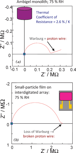 | ||
| Fig. 22 Complex impedance diagrams for manganese oxide ambigel equilibrated with 75% RH atmosphere as (a) monolith between two Pt-foil contacts; and (b) a particulate film supported on an ITO interdigitated electrode. (Adapted from ref. 196; copyright 2005, American Chemical Society.) | ||
Ion wiring in nanoarchitectures is not restricted just to protons. We also find that ceria-based pore–solid nanoarchitectures impose electrical pathways that yield macroscopic diffusion lengths for oxygen-ion transport at 600 °C. Gadolinium-doped ceria aerogels exhibit a diffusion transport path that at 0.5-mm long spans the ceramic monolith.222 The bonded transport pathways inherent to the bicontinuous pore–solid networks of these nanoarchitectures are vital to imparting these optimal electrical responses.
The fact that macroscopically long ionic nanowires are established under two such disparate physical conditions (H+ at ambient temperature and O2− at 600 °C) implies that in general, the self-wired oxide network supports electrical transport in an essentially grain-boundary-free manner. We anticipate that under the right physicochemical conditions, comparably long intranetwork paths for lithium ions can be established.
4.2 Ruggedizing the nanoarchitectural design
The tight quarters provided by the average pore size in the MnO2 ambigel architecture (currently 25 nm at best)223 was an important spur to control the synthesis and placement of the other components of the 3D nanobattery: first, the conformal, ultrathin separator/solid-polymer electrolyte, and then the interpenetrating anode. Our success, as discussed above, has also taught us important lessons about “interior design” within nanoarchitectures and contributed critical protocols and procedures to the still-young literature on assembling nanoscale building blocks to design and construct multifunctional edifices.11With the lessons learned in the cramped internal quarters of aerogel-like nanoarchitectures, we can now design a 3D battery nanoarchitecture with physical durability and more “elbow room”via building an architecture with aperiodic macroporosity (pores sized at >50 nm), rather than mesoporosity (pores sized at <50 nm). We have recently adapted the synthesis of resorcinol–formaldehyde (RF) polymer gels within a carbon-fiber paper “mold” to achieve a nanoarchitecture with nanoscopic walls expressing a “pearl necklace” morphology and pore sizes on the order of 100–200 nm.224 Upon pyrolysis of the polymeric gel at 1000 °C in an inert atmosphere, a highly conductive carbon-paper-supported carbon aerogel (or “nanofoam”) results, Fig. 23. Unsupported monoliths prepared from the same precursor polymer sol revert to standard carbon aerogel characteristics, i.e., without the “pearl necklace” morphology or desirable macropores, but with mesopores and undesirable micropores.
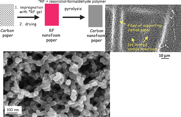 | ||
| Fig. 23 Schematic (top left) of the synthetic and processing protocol used to produce carbon-paper-supported nanofoam and scanning electron micrographs of an NRL-synthesized carbon nanofoam. The quality of the interfilling is apparent in the low magnification image (top right), while the high magnification image demonstrates the quality of macroporous network and the pearl necklace morphology of the fiber-supported carbon nanofoam (bottom). | ||
The NRL nanofoam provides three key functions to a second-generation 3D nanobattery design: (i) a rugged, practical scaffold with ample pore diameter (∼150 nm) in which to build up the active components as tricontinuous nanoscopic phases; (ii) a massively parallel aperiodic current collector, which minimizes the iR drop across modest electronically conductive cation-insertion phases; and (iii) a reactive template that serves to initiate the through-connected growth of the insertion cathode.
The insertion cathode will still be birnessite-like MnO2, but now as a conformal layer of “paint” that is electrolessly and homogeneously deposited under controlled pH conditions within and onto the fiber-supported carbon nanoarchitecture developed by Fischer et al. for electrochemical capacitor applications.120,152 The oxide–carbon hybrid nanoarchitecture can then be passivated with PPO (or the thicker varietal at ∼80 nm, PDPO) and then interfilled by lithium metal or insertion oxide colloids.
5. Specific examples of 3D electrochemical power
5.1 Electrochemical capacitors
Electrochemical capacitors fill a critical performance niche among energy-storage devices (Fig. 2), exhibiting the desirable combination of energy and power density that will ultimately enable such technologies as hybrid-electric power systems for transportation and stationary applications.225–227 Although the performance of current-generation ECs is sufficient for certain applications, future ECs will need to deliver significantly greater energy density, without sacrificing power or response time.225 Next-generation ECs will combine the best aspects of current EC materials (nanostructured carbons, conducting polymers, transition metal oxides) in new electrode compositions and cell configurations. Because the fundamental charge-storage processes utilized in ECs occur at or very near the electrode/electrolyte interface, redesigning EC electrodes as 3D multifunctional architectures will result in substantial improvements in electrochemical performance.We are applying the 3D multifunctional nanoarchitecture concept to enhance the performance of a particular type of EC in which a MnO2-based cathode is paired with a high-surface-area carbon anode in an asymmetric cell configuration with an aqueous electrolyte (neutral-pH to alkaline).228 This type of asymmetric EC has the advantages of low-cost and low-toxicity components, increased energy density relative to carbon–carbon symmetric ECs, and can deliver cell voltages up to 2 V due to the high overpotential for hydrogen evolution at the carbon anode.229 The energy and power density of such ECs are significantly improved by redesigning the MnO2 cathode as a multifunctional nanoarchitecture.
Preliminary cyclic voltammetry measurements reveal that MnO2-carbon nanofoam electrodes can exhibit the characteristics of both an electrochemical capacitor and a battery electrode. For example, when cycled between +0.5 and −0.6 V vs. Hg/HgO, the MnO2–carbon nanofoam exhibits a pseudocapacitance response, with specific (C + MnO2) capacitances of 250–300 F g−1 (Fig. 24). At potential excursions to more negative potentials (to −1.2 V), we observe distinct and reversible redox peaks. On the basis of the known MnO2 content and integrating the voltammetric currents over the range of +0.5 to −1.2 V, we find that >1.3 electrons per Mn are reversibly stored in this hybrid electrode structure. Such electrode designs will ultimately enable 2-volt aqueous asymmetric ECs that deliver energy densities >20 W h kg−1 at charge–discharge response times of <10 s.
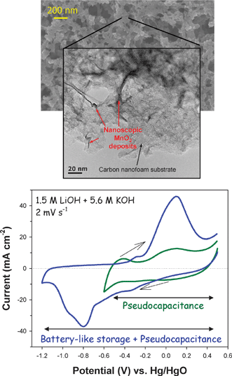 | ||
| Fig. 24 Scanning electron micrograph and transmission electron micrograph of a MnO2-coated carbon nanofoam (top and middle images, and cyclic voltammetry at 2 mV s−1 for the same electrode structure in a LiOH/KOH aqueous electrolyte. | ||
5.2 3D battery nanoarchitectures
Fabricating two thirds of the full 3D energy-storage cell (shown schematically in Fig. 25 for an aperiodic 3D nanoarchitecture) has been demonstrated by a number of groups using a range of architectural floor plans. The electrolyte-modified nanoarchitectures are then characterized in liquid electrolytes.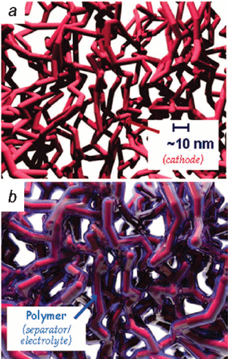 | ||
| Fig. 25 Schematic showing the conformal deposition of a separator/polymer phase over a high-surface area 3D electrode in which the functional components are sized on the order of 10 nm and are separated by 10 nm. (Adapted from ref. 11 and reproduced with permission; copyright 2007, American Chemical Society.) | ||
We have shown that sponge MnO2||PPO (with oxide walls <10 nm) can charge and discharge 55% of the unmodified Li-ion capacity at a 2C rate (i.e., full discharge of the battery in 30 min).100 Notten et al. lithographically fabricated high-aspect ratio trenches of Si (down to 50-nm thick walls) that were then conformally coated with the solid-state electrolyte LiPON (lithium phosphorous oxynitride).230,231 They found that the capacity of this 3D anode/electrolyte was maintained at ∼3600 mA g−1 while cycling in liquid electrolyte, while the stand-alone 3D Si structure suffered severe capacity fading after 30 charge–discharge cycles. Adapting 3D structures prepared for C-MEMS using SU-8 photoresist and photolithographic processing,232 high-aspect ratio arrays of 20-μm carbon posts demonstrated reversible insertion of Li+ when coated with electropolymerized dodecylbenzenesulfonate-doped polypyrrole; this assembly, however, developed electrical shorts with cycling.233
Studies illustrating the feasibility of 3D solid-state electrochemical cells are now appearing. On the micrometer scale, Peled and co-authors wall-coat 50-μm cylindrical channels with a Ni thin-film current collector and then create a concentric 3D Li-battery sandwich within the wells by electrodepositing MoS2 at the Ni, coating the MoS2 walls with a hybrid polymer electrolyte, and then interfiling the remaining core with mesoporous carbon microbeads.234–236 In comparison to a 2D arrangement of the same components in the same geometric footprint as the 3D cell, the authors measured 20–30 times higher Li-ion capacity for the 3D microbattery.234
Work with three-dimensionally interpenetrated electrode and electrolyte nanostructures has also been reported.106,107Carbon inverse opal monoliths serve as the macroporous framework and Li-ion anode of the electrochemical cell. These carbons are electrically conductive and mechanically robust without the need for added conductive phases or polymeric binders, and demonstrate rapid Li-ion insertion kinetics as compared with non-templated carbons.237 The Li-ion capacity and degree of functionality of carbon inverse opals are extended by nucleating tin(IV) oxide nanoparticles onto the ordered macropore walls.
Using the strategy developed by Rhodes et al.,99 ultrathin PPO coatings are subsequently electrodeposited at all electrifiable interfaces within the carbon inverse-opal electrodes in order to create a polymer film that conforms to the 3D nanoarchitecture without plugging pores. The polymer simultaneously serves as a solid-state Li-ion electrolyte (after impregnation with LiClO4 and thermal annealing) and dielectric separator, one that can withstand the extreme electric fields of a nanoscopic Li-ion electrochemical cell.99,106,107
The remaining macropore volume in the carbon–polymer composite is then fully infused with a continuous network of vanadia xerogel,238 which serves as the Li-ion cathode in the completed cell. Carbon–polymer composite architectures were repeatedly vacuum-infiltrated with vanadium tri-isopropoxide, and then controllably aged to induce gradual gelation. The carbon anode in the fully infiltrated composite was electrochemically lithiated, and the complete cell cycled between 0.4–3.3 V. The performance of this prototype reveals major challenges with (i) the electronic conductivity of the vanadia cathode; (ii) the fact that charge storage more closely resembles pseudocapacitance rather than battery-like ion insertion; and (iii) limited mobility of ionic charges through the PPO electrolyte/separator. A major boost in this cell’s specific capacity (from 0.7 to ∼350 μA h g−1) was recently reported as achieved by ambiently drying the vanadia gel cathode.
5.3 Fuel cells
Fuel-cell technologies hold great promise for energy conversion because they deliver energy densities that are orders of magnitude greater than conventional batteries and capacitors, most closely approximate the power and energy densities of internal combustion engines, and can be powered with renewable fuels. The U.S. Department of Energy has targeted large-scale fuel cell manufacturing at $30 USD kW−1 by 2015,239 but present commercialization costs are prohibitive, in part because of the high market price of precious metals. One approach to cutting these costs is to utilize those metals more judiciously in the first place, which is why fuel-cell electrocatalysts rely on the high surface-to-volume ratio of nanoparticles.Ultraporous nanoarchitectures innately function as fuel-cell electrode scaffolds in which one can incorporate catalytic nanoparticles at massively parallel interfaces and create a three-phase boundary where fuel molecules, electrons, and ions converge—all on a minimal geometric footprint. Che et al. recognized the elegant applicability of carbon nanotubule arrays as electrochemical energy platforms and demonstrated their ability to support electrocatalytic Pt nanoparticles for oxygen reduction, Pt–Ru nanoparticles for methanol oxidation, and to serve as nanoscopic Li-ion insertion electrodes.240
Multifunctionality is also afforded by creating electron-rich moieties that covalently link active catalytic nanoparticles to underlying nanoarchitectures: Pt nanoparticles are molecularly anchored at thiophenyl165 functionalities that are grafted onto ultraporous phenolic resins and at hydroxyl,241carbonyl, and carboxyl groups that are created by etching carbon nanotubes in strong acids. Introducing additional functionality into carbon and other electrode architectures by incorporating metals and metal oxides can enhance or even completely alter existing electron-transfer kinetics and reaction pathways. The performance of direct methanol fuel cells is increased by incorporating hydrous ruthenium oxide242,243 at the three-phase boundary of carbon nanotube electrode arrays in order to conduct both electrons and protons to nearby Pt catalysts.244 Likewise, other transition metals and alloys selectively electrocatalyze additional energy conversion reactions: Palladium and Pd–Ir electrocatalysts supported on carbon fiber arrays245 and nickel foams246 electrocatalytically reduce hydrogen peroxide in magnesium semi-fuel cell environments and electro-oxidize formic acid.247
Furthermore, electrode architectures can be retrofitted with physical properties that benefit their use in fuel-cell applications. Electrocatalytic activity and mechanical robustness are symbiotically combined by anchoring catalytic transition metal nanoparticles to thiophenyl sites on Vulcan carbon particles and subsequently using a silica sol to nanoglue248 the carbon–metal composites into a monolithic electrode.3 Multifunctional composites comprising single-walled carbon nanotubes, PTFE, and Pt nanoparticles can serve as both cathode and anode in hydrogen fuel cells and are their own gas-diffusion layers, catalytic supports, and nanoscale current collectors.249
5.4 Photovoltaics in 3D
Photovoltaic devices are another example where several functionalities—electron conduction, hole conduction, photon absorption, interfacial charge transfer—must be carefully engineered into the underlying structures in order to optimize power conversion efficiency. When moving beyond more conventional silicon-based p- and n-type photovoltaic devices, rethinking electrode design in terms of a multifunctional architecture becomes even more critical, for example with new photovoltaic cell designs based on bulk heterojunctions. Such systems are typically based on interpenetrating networks of distinct electron and hole-conducting phases, where the extensive 3D interface results in substantially improved conversion efficiency.250–252 However, diffusion of the photogenerated exciton (i.e., an electron–hole pair) is often the limiting process, and thus there is a delicate balance between maximizing donor–acceptor interfaces and also providing for efficient charge transport through the interpenetrating phases.Photovoltaic cells based on organic bulk heterojunctions typically comprise conjugated polymers serving as electron-donating hole conductors and C60 derivatives acting as electron acceptors.250,253,254 Such systems are optimized when the composite material is fabricated as a hierarchical structure of small polymer domains (∼10 nm) that are incorporated with agglomerated C60 derivatives (∼50–200 nm). By limiting the size of the polymer component to less than the photoexcitation diffusion length, collection of incoming photons is maximized, while the C60 domains facilitate efficient electron transport.253 Efficiencies of 2.2% have been achieved with this design.253,255
Replacing the fullerene with an inorganic n-type semiconductor creates a hybrid organic–inorganic photovoltaic device that still takes advantage of the 3D heterojunction design. Examples of such n-type semiconductors include TiO2,256 CdS,257ZnO, SnO2, Nb2O5, CeO2 and CdSe,258 many of which can be fabricated in 3D nanostructured forms such as oriented nanorods,259–261 inverse opals,262 and nanotubes. 251 Efficiencies of up to 1.7% have been reported for bulk heterojunction devices comprising 3D architectures of these n-type semiconductors that also incorporate an electron-donating polymer.257 A higher efficiency of 4.1% can be achieved using a double-heterojunction design based on a TiO2nanotube array interfilled with both poly(3-hexylthiophene) and a methanofullerene (see Fig. 26).251 This general design concept can be extended to Grätzel-type dye-sensitized solar cells,263 for example by infiltrating a hole-transport polymer into an ordered macroporous TiO2 architecture pre-modified with a ruthenium-based sensitizer.264 In the case of both organic and hybrid inorganic–organic 3D heterojunction designs, many challenges remain in terms of controlling the spatial distribution of the individual components and characterizing the complex structures of the resulting nanoarchitectures.
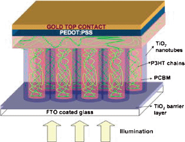 | ||
| Fig. 26 Illustration showing a double-heterojunction device configuration. (Reproduced with permission from ref. 251; copyright 2007, American Institute of Physics.) | ||
A p-type absorber and hole-conducting semiconductor can replace the polymer in hybrid cells or the dye and hole conductor in dye-sensitized cells. For example, copper indium sulfide (CuInS2) was deposited into a porous TiO2electrode using ALD to produce a solar cell that can respond 1000 times faster than conventional dye-sensitized cells.265 Even conventional silicon-based solar cells can benefit from 3D architecture. Incorporating p–n junctions into porous silicon can increase efficiencies up to 10 times that of similar planar diodes.252 Higher concentrations of dopant can be achieved in porous silicon, decreasing resistance and increasing efficiency.
6. Future outlook
The full potential of electrochemical power sources based on multifunctional 3D nanoarchitectures has yet to be realized, but as outlined in this review, a strong foundation for future advances is now established. Innovative fabrication approaches have been developed and adapted specifically to create complex 3D architectures and prototype 3D architectures for key applications are now demonstrated. Many challenges remain, particularly with regard to characterizing and understanding the physical, chemical, and electrochemical interactions within multicomponent nanoscale systems. Ultimately, well-designed multifunctional 3D nanoarchitectures will serve as the basis for microscale batteries, next-generation electrochemical capacitors, fuel-cell architectures, and advanced photovoltaic cells, all of which will exhibit significant performance advantages over current state-of-the-art technologies in their respective fields.Acknowledgements
The authors gratefully acknowledge the US Office of Naval Research and the US Defense Applied Research Projects Agency for support of our program on multifunctional nanoarchitectures.References
- J. O’M. Bockris and A. K. N. Reddy, Modern Electrochemistry 2, Plenum, New York, 1970, p. 694 Search PubMed.
- D. R. Rolison, in Nanotechnology and the Environment, ed. B. Karn, T. Masciangioli, W.-X. Zhang, V. Colvin and A. P. Alivisatos, Oxford University Press, Oxford, UK, 2004, ACS Symp. Ser., vol. 890, pp. 324–330 Search PubMed.
- M. L. Anderson, R. M. Stroud and D. R. Rolison, Nano Lett., 2002, 2, 235–240 CrossRef [correction: Nano Lett., 2003, 3, 1321].
- J. Hockenberry, Wired, 2006, 14(11) Search PubMed http://www.wired.com/wired/archive/14.11/battery.html .
- B. B. Owens and T. Osaka, J. Power Sources, 1997, 68, 173–186 CrossRef.
- Basic Research Needs for Electrical Energy Storage, Office of Basic Sciences, Department of Energy, 2007, p. 18, 〈http://www.sc.doe.gov/bes/reports/files/EES_rpt.pdf〉 Search PubMed.
- R. W. Hart, H. S. White, B. Dunn and D. R. Rolison, Electrochem. Commun., 2003, 5, 120–123 CrossRef CAS.
- J. W. Long, B. Dunn, D. R. Rolison and H. S. White, Chem. Rev., 2004, 104, 4463–4492 CrossRef CAS.
- B. Dunn, J. W. Long and D. R. Rolison, Interface, 2008, 17(3), 49–53 Search PubMed.
- D. R. Rolison, Science, 2003, 299, 1698–1701 CrossRef CAS.
- J. W. Long and D. R. Rolison, Acc. Chem. Res., 2007, 40, 854–862 CrossRef CAS.
- L. Doherty, B. A. Warneke, B. E. Boser and K. S. J. Pister, Int. J. Parallel Distr. Syst. Networks, 2001, 4, 121–133 Search PubMed.
- B. Warnike, M. Last, B. Liebowitz and K. S. J. Pister, Computer, 2001, 34, 44–51 CrossRef.
- S. Roundy, D. Steingart, L. Frechette, P. Wright and J. Rabaey, Proc. Wireless Sensor Networks, 2004, 2920, 1–17 Search PubMed.
- D. R. Rolison and B. Dunn, J. Mater. Chem., 2001, 11, 963–980 RSC.
- N. Hüsing and U. Schubert, Angew. Chem., Int. Ed., 1998, 37, 23–45.
- N. Leventis, I. A. Elder, D. R. Rolison, M. L. Anderson and C. I. Merzbacher, Chem. Mater., 1999, 11, 2837–2845 CrossRef CAS.
- J. M. Wallace, J. K. Rice, J. J. Pietron, R. M. Stroud, J. W. Long and D. R. Rolison, Nano Lett., 2003, 3, 1463–1467 CrossRef CAS.
- M. Putkonen, J. Harjuoja, T. Sajavaara and L. Niinistö, J. Mater. Chem., 2007, 17, 664–669 RSC.
- J. Jang and B. Lim, Angew. Chem., Int. Ed., 2003, 42, 5600–5603 CrossRef CAS.
- W. E. Tenhaeff and K. K. Gleason, Adv. Funct. Mater., 2008, 18, 979–992 CrossRef CAS.
- N. M. Adamczyk, A. A. Dameron and S. M. George, Langmuir, 2008, 24, 2081–2089 CrossRef CAS.
- D.-Y. Yang, S. H. Park, T. W. Lim, H.-J. Kong, S. W. Yi, H. K. Yang and K.-S. Lee, Adv. Phys. Lett., 2007, 90, 013113/1 Search PubMed.
- D. J. Shir, S. Jeon, H. Liao, M. Highland, D. G. Cahill, M. F. Su, I. F. El-Kady, C. G. Christodoulou, G. R. Bogart, A. V. Hamza and J. A. Rogers, J. Phys. Chem. B, 2007, 111, 12945–12958 CrossRef CAS.
- P. T. Hammond, Adv. Mater., 2004, 16, 1271–1293 CrossRef CAS.
- P. Bertrand, A. Jonas, A. Laschewsky and R. Legras, Macromol. Rapid Commun., 2000, 21, 319–348 CrossRef CAS.
- D. M. Lynn, Adv. Mater., 2007, 19, 4118–4130 CrossRef CAS.
- G. Decher and J.-D. Hong, Ber. Bunsen-Ges., 1991, 95, 1430–1434 CAS.
- Y. Wang, A. S. Angelatos and F. Caruso, Chem. Mater., 2008, 20, 848–858 CrossRef CAS.
- J. J. Harris, J. L. Stair and M. L. Bruening, Chem. Mater., 2000, 12, 1941–1946 CrossRef CAS.
- A. A. Argun, J. N. Ashcraft and P. T. Hammond, Adv. Mater., 2008, 20, 1539–1543 CrossRef CAS.
- D. M. DeLongchamp and P. T. Hammond, Langmuir, 2004, 20, 5403–5411 CrossRef CAS.
- J. L. Lutkenhaus and P. T. Hammond, Soft Matter, 2007, 3, 804–816 RSC.
- K. T. Nam, D.-W. Kim, P. J. Yoo, C.-Y. Chiang, N. Meethong, P. T. Hammond, Y.-M. Chiang and A. M. Belcher, Science, 2006, 312, 885–888 CrossRef CAS.
- C. Ge, N. R. Armstrong and S. S. Saavedra, Anal. Chem., 2007, 79, 1401–1410 CrossRef CAS.
- F. Caruso, R. A. Caruso and H. Möhwald, Science, 1998, 282, 1111–1114 CrossRef CAS.
- C. R. Martin, Adv. Mater., 1991, 3, 457–459 CrossRef CAS.
- R. V. Parthasarathy and C. R. Martin, Chem. Mater., 1994, 6, 1627–1632 CrossRef.
- S. Hou, C. C. Harrell, L. Trofin, P. Kohli and C. R. Martin, J. Am. Chem. Soc., 2004, 126, 5674–5675 CrossRef CAS.
- Z. Liang, A. S. Susha, A. Yu and F. Caruso, Adv. Mater., 2003, 15, 1849–1853 CrossRef CAS.
- C. R. Martin, Science, 1994, 266, 1961–1966 CrossRef CAS.
- Y. K. Cho, R. Wartena, S. M. Tobias and Y.-M. Chiang, Adv. Funct. Mater., 2007, 17, 379–389 CrossRef CAS.
- E. M. Lifshitz, Sov. Phys. JETP, 1956, 2, 73–83.
- C. J. van Oss, R. J. Good and M. K. Chaudhury, Langmuir, 1988, 4, 884–891 CrossRef CAS.
- L. Weinstein, W. Yourey, J. Gural and G. G. Amatucci, J. Electrochem. Soc., 2008, 155, A590–A598 CrossRef CAS.
- J. E. Herrera, J. H. Kwak, J. H. Yong and C. H. Peden, Top. Catal., 2006, 39, 245–255 CrossRef CAS.
- M. Knez, Mater. Matters, 2008, 3(2), 28–30 Search PubMed.
- J. Biener, T. F. Baumann, Y. Wang, E. J. Nelson, S. O. Kucheyev, A. V. Hamza, M. Kemmell, M. Ritala and M. Keskela, Nanotechnology, 2007, 18, 055303 CrossRef.
- J. W. Elam, J. A. Libera, M. J. Pellin, A. V. Zinovev, J. P. Greene and J. A. Nolen, Appl. Phys. Lett., 2006, 89, 053124 CrossRef.
- J. S. King, A. Wittstock, J. Biener, S. O. Kucheyev, Y. M. Wang, T. F. Baumann, S. K. Giri, A. V. Hamza, M. Baeumer and S. F. Bent, Nano Lett., 2008, 8, 2405–2409 CrossRef CAS.
- S. O. Kucheyev, J. Biener, T. F. Baumann, Y. M. Wang, A. V. Hamza, Z. Li, D. K. Lee and R. G. Gordon, Langmuir, 2008, 24, 943–948 CrossRef CAS.
- S. O. Kucheyev, J. Biener, Y. M. Wang, T. F. Baumann, K. J. Wu, T. van Buuren, A. V. Hamza, J. H. Satcher, Jr, J. W. Elam and M. J. Pellin, Appl. Phys. Lett., 2005, 86, 083108 CrossRef.
- T. F. Baumann, J. Biener, Y. M. Wang, S. O. Kucheyev, E. J. Nelson, J. H. Satcher, Jr, J. W. Elam, M. J. Pellin and A. V. Hamza, Chem. Mater., 2006, 18, 6106–6108 CrossRef CAS.
- G.-M. Kim, S.-M. Lee, G. H. Michler, H. Roggendorf, U. Gosele and M. Knez, Chem. Mater., 2008, 20, 3085–3091 CrossRef CAS.
- J. S. King, E. Graugnard, O. M. Roche, D. N. Sharp, J. Scrimgeour, R. G. Denning, A. J. Turberfield and C. J. Summers, Adv. Mater., 2006, 18, 1561–1565 CrossRef CAS.
- J. W. Elam, J. A. Libera, M. J. Pellin and P. C. Stair, Appl. Phys. Lett., 2007, 91, 243105 CrossRef.
- J. W. Elam, A. Zinovev, C. Y. Han, H. H. Wang, U. Welp, J. N. Hryn and M. J. Pellin, Thin Solid Films, 2006, 515, 1664–1673 CrossRef CAS.
- M. J. Pellin, P. C. Stair, G. Xiong, J. W. Elam, J. Birrell, L. Curtiss, S. M. George, C. Y. Han, L. Iton, H. Kung, M. Kung and H. H. Wang, Catal. Lett., 2005, 102, 127–130 CrossRef CAS.
- J. S. King, E. Graugnard and C. J. Summers, Adv. Mater., 2005, 17, 1010–1013 CrossRef CAS.
- J. S. King, C. W. Neff, C. J. Summers, W. Park, S. Blomquist, E. Forsythe and D. Morton, Appl. Phys. Lett., 2003, 83, 2566–2568 CrossRef CAS.
- B. A. McCool and W. J. DeSisto, Chem. Vap. Deposition, 2004, 10, 190–194 CrossRef CAS.
- P. C. Stair, C. Marshall, G. Xiong, H. Feng, M. J. Pellin, J. W. Elam, L. Curtiss, L. Iton, H. Kung, M. Kung and H. H. Wang, Top. Catal., 2006, 39, 181–186 CrossRef CAS.
- P. Chen, T. Misui, D. B. Farmer, J. Golovchenko, R. G. Gordon and D. Branton, Nano Lett., 2004, 4, 1333–1337 CrossRef CAS.
- A. Rugge, J. S. Becker, R. G. Gordon and S. H. Tolbert, Nano Lett., 2003, 3, 1293–1297 CrossRef CAS.
- V. Miikkulainen, T. Rasilainen, E. Puukilainen, M. Suvanto and T. A. Pakkanen, Langmuir, 2008, 24, 4473–4477 CrossRef CAS.
- M. Leskela, M. Kemell, K. Kukli, V. Pore, E. Santala, M. Ritala and J. Lu, Mater. Sci. Eng. C, 2007, 27, 1504–1508 CrossRef.
- F. Zaera, J. Mater. Chem., 2008, 18, 3521–3526 RSC.
- H. Miguez, N. Tetreault, B. Hatton, S.-M. Yang, D. Perovic and G. A. Ozin, Chem. Commun., 2002, 2736–2737 RSC.
- J. W. Long, C. P. Rhodes, A. L. Young and D. R. Rolison, Nano Lett., 2003, 3, 1155–1161 CrossRef CAS.
- A. A. Syed and M. K. Dinesan, Talanta, 1991, 38, 815–837 CrossRef CAS.
- G. Inzelt, M. Pineri, J. W. Schultze and M. A. Vorotyntsev, Electrochim. Acta, 2000, 45, 2403–2421 CrossRef CAS.
- A. E. Fischer, T. M. McEvoy and J. W. Long, Electrochim. Acta, in review.
- H. Talbi, P.-E. Just and L. H. Dao, J. Appl. Electrochem., 2003, 33, 465–473 CrossRef CAS.
- S. Leinad Gnana Lissy, S. Pitchumani and K. Jayakumar, Mater. Chem. Phys., 2002, 76, 143–150 CrossRef CAS.
- D. Bélanger, X. Ren, J. Davey, F. Uribe and S. Gottesfeld, J. Electrochem. Soc., 2000, 147, 2923–2929 CrossRef CAS.
- F. Fusalba, P. Gouérec, D. Villers and D. Bélanger, J. Electrochem. Soc., 2001, 148, A1–A6 CrossRef CAS.
- W.-C. Chen, T.-C. Wen and H. Teng, Electrochim. Acta, 2003, 48, 641–649 CrossRef CAS.
- C.-C. Hu and C.-H. Chu, J. Electroanal. Chem., 2001, 503, 105–116 CrossRef CAS.
- Y. Miao, J. Chen and X. Wu, Trends Biotechnol., 2004, 22, 227–231 CrossRef CAS.
- P. N. Bartlett and J. M. Cooper, J. Electroanal. Chem., 1993, 362, 1–12 CrossRef CAS.
- D. Pan, J. Chen, S. Yao, W. Tao and L. Nie, Anal. Sci., 2005, 21, 367–371 CrossRef CAS.
- Z. E. Zhang, H. Liu and J. Deng, Anal. Chem., 1996, 68, 1632–1638 CrossRef CAS.
- L. Duić and Z. Mandić, J. Electroanal. Chem., 1992, 335, 207–221 CrossRef CAS.
- A. M. Yacynych and H. B. Mark, J. Electrochem. Soc., 1976, 123, 1346–1351 CrossRef CAS.
- H. J. Wieck and A. M. Yacynych, Anal. Chem., 1980, 52, 345–346 CrossRef CAS.
- S. Emr and A. M. Yacynych, Electroanalysis, 1995, 7, 913–923 CAS.
- I. Losito, E. De Giglio, N. Cioffi and C. Malitesta, J. Mater. Chem., 2001, 11, 1812–1817 RSC.
- I. Losito, F. Palmisiano and P. G. Zambonin, Anal. Chem., 2003, 75, 4988–4995 CrossRef CAS.
- C.-C. Wu and H.-C. Chang, Anal. Chim. Acta, 2004, 505, 239–246 CrossRef CAS.
- I. Losito, N. Cioffi, M. Pia Vitale and F. Palmisano, Rapid Commun. Mass Spectrom., 2003, 17, 1169–1179 CrossRef CAS.
- T. M. McEvoy, J. W. Long, T. J. Smith and K. J. Stevenson, Langmuir, 2006, 22, 4462–4466 CrossRef CAS.
- J. W. Long, B. M. Dening, T. M. McEvoy and D. R. Rolison, J. Non-Cryst. Solids, 2004, 350, 97–106 CrossRef CAS.
- A. E. Fischer, M. P. Saunders, J. C. Lytle, D. R. Rolison and J. W. Long, ECS Trans., 2008, 6, 159–164 Search PubMed.
- J. M. Ortega, S. Menolasina, O. Pérez de Márquez and J. Márquez, Polymer, 1986, 27, 1304–1306 CrossRef CAS.
- S. L. Cram, G. M. Spinks, G. G. Wallace and H. R. Brown, Electrochim. Acta, 2002, 47, 1935–1948 CrossRef CAS.
- R. L. McCarley, R. E. Thomas, E. A. Irene and R. W. Murray, J. Electroanal. Chem., 1990, 290, 79–92 CrossRef CAS.
- R. L. McCarley, E. A. Irene and R. W. Murray, J. Phys. Chem., 1991, 95, 2492–2498 CrossRef.
- N. Oyama, T. Ohsaka, Y. Ohnuki and T. Suzuki, J. Electrochem. Soc., 1987, 134, 3068–3073 CAS.
- C. P. Rhodes, J. W. Long, M. S. Doescher, J. J. Fontanella and D. R. Rolison, J. Phys. Chem. B, 2004, 108, 13079–13087 CrossRef CAS.
- C. P. Rhodes, J. W. Long, M. S. Doescher, B. M. Dening and D. R. Rolison, J. Non-Cryst. Solids, 2004, 350, 73–79 CrossRef CAS.
- P. V. Wright, MRS Bull., 2002, 27, 597–602 CAS.
- K. S. Nahm and A. M. Stephan, Polymer, 2006, 16, 5952–5964.
- C. P. Rhodes, J. W. Long and D. R. Rolison, Electrochem. Solid-State Lett., 2005, 8, A579–A584 CrossRef CAS.
- E. Granot, R. Tel-Vered, O. Lioubashevski and I. Willner, Adv. Funct. Mater., 2008, 18, 478–484 CrossRef CAS.
- K. P. Loh, S. L. Zhao and W. D. Zhang, Diamond Related Mater., 2004, 13, 1075–1079 CrossRef CAS.
- N. S. Ergang, J. C. Lytle, K. T. Lee, S. M. Oh and A. Stein, Adv. Mater., 2006, 18, 1750–1753 CrossRef CAS.
- N. S. Ergang, M. A. Fierke, Z. Wang, W. H. Smyrl and A. Stein, J. Electrochem. Soc., 2007, 154, A1135–A1139 CrossRef CAS.
- P. C. Andricacos, Interface, 1999, 8(1), 32–37 Search PubMed.
- P. C. Andricacos, C. Uzoh, J. O. Dukovic, J. Horkans and H. Deligianni, IBM J. Res. Dev., 1998, 42, 567–574 CrossRef CAS.
- J. L. Stickney, Adv. Electrochem. Sci. Eng., 2000, 7, 1–105 Search PubMed.
- V. Venkatasamy, N. Jayaraju, S. M. Cox, C. Thambidurai and J. L. Stickney, J. Electrochem. Soc., 2007, 154, H720–H725 CrossRef CAS.
- C. Thambidurai, Y. G. Kim and J. L. Stickney, Electrochim. Acta, 2008, 53, 6157–6164 CrossRef CAS.
- J. P. Zheng and T. R. Jow, J. Electrochem. Soc., 1995, 142, L6–L8 CAS.
- T. R. Jow and J. P. Zheng, J. Electrochem. Soc., 1998, 145, 49–52 CAS.
- J. P. Zheng, P. J. Cygan and T. R. Jow, J. Electrochem. Soc., 1995, 142, 2699–2703 CAS.
- K. E. Swider, C. I. Merzbacher, P. L. Hagans and D. R. Rolison, Chem. Mater., 1997, 9, 1248–1255 CrossRef CAS.
- W. C. Fang, J. H. Huang, L. C. Chen, Y. L. O. Su and K. H. Chen, J. Power Sources, 2006, 160, 1506–1510 CrossRef CAS.
- B. O. Park, C. D. Lokhande, H. S. Park, K. D. Jung and O. S. Joo, Mater. Chem. Phys., 2004, 87, 59–66 CrossRef CAS.
- http://www.thebulliondesk.com/ .
- A. E. Fischer, K. A. Pettigrew, D. R. Rolison, R. M. Stroud and J. W. Long, Nano Lett., 2007, 7, 281–286 CrossRef CAS.
- M. Toupin, T. Brousse and D. Bélanger, Chem. Mater., 2004, 16, 3184–3190 CrossRef CAS.
- V. Subramanian, H. Zhu, R. Vajtai, P. M. Ajayan and B. Wei, J. Phys. Chem. B, 2005, 109, 20207–20214 CrossRef CAS.
- S. C. Pang, M. A. Anderson and T. W. Chapman, J. Electrochem. Soc., 2000, 147, 444–450 CAS.
- X. Huang, H. Yue, A. Attia and Y. Yang, J. Electrochem. Soc., 2007, 154, A26–A33 CrossRef CAS.
- S. B. Ma, K. Y. Ahn, E. S. Lee, K. H. Oh and K. B. Kim, Carbon, 2007, 45, 375–382 CrossRef CAS.
- X. Dong, W. Shen, J. Gu, L. Xiong, Y. Zhu, H. Li and J. Shi, J. Phys. Chem. B, 2006, 110, 6015–6019 CrossRef CAS.
- J. N. Broughton and M. J. Brett, Electrochim. Acta, 2004, 49, 4439–4446 CrossRef CAS.
- M. Wu, G. A. Snook, G. Z. Chen and D. J. Fray, Electrochem. Commun., 2004, 6, 499–504 CrossRef CAS.
- N. L. Wu, S. Y. Wang, C. Y. Han, D. S. Wu and L. R. Shiue, J. Power Sources, 2003, 113, 173–178 CrossRef CAS.
- T. Cottineau, M. Toupin, T. Delahaye, T. Brousse and D. Bélanger, Appl. Phys. A, 2006, 82, 599–606 CrossRef CAS.
- S. Y. Wang and N. L. Wu, J. Appl. Electrochem., 2003, 33, 345–348 CrossRef CAS.
- N. Nagarajan and I. Zhitomirsky, J. Appl. Electrochem., 2006, 36, 1399–1405 CrossRef CAS.
- K.-C. Liu and M. A. Anderson, J. Electrochem. Soc., 1996, 143, 124–130 CrossRef CAS.
- P. A. Nelson and J. R. Owen, J. Electrochem. Soc., 2003, 150, A1313–A1317 CrossRef CAS.
- E. E. Kalu, T. T. Nwoga, V. Srinivasan and J. W. Weidner, J. Power Sources, 2001, 92, 163–167 CrossRef CAS.
- V. Srinivasan and J. W. Weidner, J. Electrochem. Soc., 1997, 144, L210–L213 CAS.
- C. Lin, J. A. Ritter and B. N. Popov, J. Electrochem. Soc., 1998, 145, 4097–4103 CrossRef CAS.
- V. R. Shinde, S. B. Mahadik, T. P. Gujar and C. D. Lokhande, Appl. Surf. Sci., 2006, 252, 7487–7492 CrossRef CAS.
- S. G. Kandalkar, C. D. Lokhande, R. S. Mane and S.-H. Han, Appl. Surf. Sci., 2007, 253, 3952–3956 CrossRef CAS.
- Y. Li, B. Tan and Y. Wu, Nano Lett., 2008, 8, 265–270 CrossRef CAS.
- C.-C. Hu and T.-Y. Hsu, Electrochim. Acta, 2008, 53, 2386–2395 CrossRef CAS.
- N.-L. Wu, Mater. Chem. Phys., 2002, 75, 6–11 CrossRef CAS.
- K. R. Prasad and N. Miura, Electrochem. Commun., 2004, 6, 849–852 CrossRef CAS.
- S.-W. Hwang and S.-H. Hyun, J. Power Sources, 2007, 172, 451–459 CrossRef CAS.
- M. Wu, L. Zhang, D. Wang, C. Xiao and S. Zhang, J. Power Sources, 2008, 175, 669–674 CrossRef CAS.
- A. Leela Mohana Reddy and S. Ramaprabhu, J. Phys. Chem. C, 2007, 111, 7727–7734 CrossRef CAS.
- R. Kalai Selvan, I. Perelshtein, N. Perkas and A. Gedanken, J. Phys. Chem. C, 2008, 112, 1825–1830 CrossRef CAS.
- K. Naoi and P. Simon, Interface, 2008, 17(1), 34–37 Search PubMed.
- J. W. Long, K. E. Swider, C. I. Merzbacher and D. R. Rolison, Langmuir, 1999, 15, 780–785 CrossRef CAS [correction: Langmuir, 2003, 19, 2532].
- Y. Liu, C. Mi, L. Su and X. Zhang, Electrochim. Acta, 2008, 53, 2507–2513 CrossRef CAS.
- D. Susanti, D.-S. Tsai, Y.-S. Huang, A. Korotcov and W.-H. Chung, J. Phys. Chem. C, 2007, 111, 9530–9537 CrossRef CAS.
- A. E. Fischer, M. P. Saunders, K. A. Pettigrew, D. R. Rolison and J. W. Long, J. Electrochem. Soc., 2008, 155, A246–A252 CrossRef CAS.
- J. F. Perez-Bentio, C. Arias and E. Brillas, Int. J. Chem. Kinet., 1990, 22, 261–287 CrossRef CAS.
- K. A. Kovács, P. Gróf, L. Burai and M. Riedel, J. Phys. Chem. A, 2004, 108, 11026–11031 CrossRef.
- J. V. Ryan, A. D. Berry, M. L. Anderson, J. W. Long, R. M. Stroud, V. M. Cepak, V. M. Browning, D. R. Rolison and C. I. Merzbacher, Nature, 2000, 406, 169–172 CrossRef CAS.
- J. W. Long, C. P. Rhodes, J. C. Lytle, K. A. Pettigrew, R. M. Stroud and D. R. Rolison, Prepr. Pap.-Am. Chem. Soc., Div. Fuel Chem., 2006, 51(1), 41–43 Search PubMed.
- C. P. Rhodes, J. W. Long, R. M. Stroud, K. A. Pettigrew and D. R. Rolison, in preparation for publication.
- S. N. Li, P. G. He, J. H. Dong, Z. X. Guo and L. M. Dai, J. Am. Chem. Soc., 2004, 127, 14–15.
- B. C. Satishkumar, E. M. Vogl, A. Govindaraj and C. N. R. Rao, J. Phys. D: Appl. Phys., 1996, 29, 3173–3176 CrossRef CAS.
- J. Liu, A. G. Rinzler, H. Dai, J. H. Hafner, R. K. Bradley, P. J. Boul, A. Lu, T. Iverson, K. Shelimov, C. B. Huffman, F. Rodriguez-Macias, Y.-S. Shon, T. R. Lee, D. T. Colbert and R. E. Smalley, Science, 1998, 280, 1253–1256 CrossRef CAS.
- K. Jiang, A. Eitan, L. S. Schadler, P. M. Ajayan, R. W. Siegel, N. Grobert, M. Mayne, M. Reyes-Reyes, H. Terrones and M. Terrones, Nano Lett., 2003, 3, 275–277 CrossRef CAS.
- M. Watanabe, M. Uchida and S. Motoo, J. Electroanal. Chem., 1987, 229, 395–406 CrossRef CAS.
- D. L. Boxall, G. A. Deluga, E. A. Kenik, W. D. King and C. M. Lukehart, Chem. Mater., 2001, 13, 891–900 CrossRef CAS.
- K. E. Swider and D. R. Rolison, J. Electrochem. Soc., 1996, 143, 813–819 CrossRef CAS.
- W. S. Baker, J. W. Long, R. M. Stroud and D. R. Rolison, J. Non-Cryst. Solids, 2004, 350, 80–87 CrossRef CAS.
- S. C. Roy, P. A. Christensen, A. Hamnett, K. M. Thomas and V. Trapp, J. Electrochem. Soc., 1996, 143, 3073–3079 CrossRef CAS.
- S. C. Roy, A. W. Harding, A. E. Russell and K. M. Thomas, J. Electrochem. Soc., 1997, 144, 2323–2328 CAS.
- C. Arbizzani, S. Beninati, E. Manferrari, F. Soavi and M. Mastragostino, J. Power Sources, 2007, 172, 578–586 CrossRef CAS.
- C. D. Saquing, T.-T. Cheng, M. Aindow and C. Erkey, J. Phys. Chem. B, 2004, 108, 7716–7722 CrossRef CAS.
- I. Arslan, T. J. V. Yates, N. D. Browning and P. A. Midgley, Science, 2005, 309, 2195–2198 CrossRef CAS.
- A. I. Frenkel, S. Nemzer, I. Pister, L. Soussan, T. Harris, Y. Sun and M. H. Rafailovich, Chem. Phys., 2005, 123, 184701 CAS.
- B. Gilbert, F. Huang, H. Z. Zhang, G. A. Waychunas and J. F. Banfield, Science, 2004, 305, 651–654 CrossRef CAS.
- C. Roth, N. Martz and H. Fuess, J. New Mater. Electrochem. Syst., 2004, 7, 117–123 Search PubMed.
- K. S. W. Sing, Colloids Surf. A, 2004, 241, 3–7 CrossRef CAS.
- K. S. W. Sing, Adv. Colloid Interface Sci., 1998, 77, 3–11 CrossRef.
- C. P. Grey and Y. J. Lee, Solid State Sciences, 2003, 5, 883–894 CrossRef CAS.
- J. W. Long, K. E. Ayers and D. R. Rolison, J. Electroanal. Chem., 2002, 522, 58–65 CrossRef CAS.
- W. Dong, B. Dunn and D. R. Rolison, Electrochem. Solid-State Lett., 2000, 3, 457–459 CrossRef CAS.
- J. C. Lytle, C. P. Rhodes, J. W. Long, K. A. Pettigrew, R. M. Stroud and D. R. Rolison, J. Mater. Chem., 2007, 17, 1292–1299 RSC.
- Film thickness was determined using AFM; the error on these values is ±2 nm.
- S. Patil, J. R. Mahajan, M. A. More and P. P. Patil, Mater. Lett., 1998, 35, 108–115 CrossRef CAS.
- S. Patil, J. R. Mahajan, M. A. More, P. P. Patil, S. W. Gosavi and S. A. Gangal, Polym. Int., 1998, 46, 99–105 CrossRef CAS.
- R. Vera, R. Schrebler, P. Cury, R. Del Rio and H. Romero, J. Appl. Electrochem., 2007, 37, 519–525 CrossRef CAS.
- M.-I. Boyer, S. Quillard, E. Rebourt, G. Louran, J. P. Buisson, A. Monkman and S. Lefrant, J. Phys. Chem. B, 1998, 102, 7382–7392 CrossRef CAS.
- C. P. Collier, E. W. Wong, M. Belohradsky, F. M. Raymo, J. F. Stoddart, P. J. Kuekes, R. S. Williams and J. R. Heath, Science, 1999, 285, 391–394 CrossRef CAS.
- R. M. Metzger, T. Xu and I. R. Peterson, J. Phys. Chem. B, 2001, 105, 7280–7290 CrossRef CAS.
- B. de Boer, M. M. Frank, Y. J. Chabal, W. R. Jiang, E. Garfunkel and Z. Bao, Langmuir, 2004, 20, 1539–1542 CrossRef CAS.
- R. C. Chiechi, E. A. Weiss, M. D. Dickey and G. M. Whitesides, Angew. Chem., Int. Ed., 2008, 46, 1–4.
- T. Egami, J. Phys. Chem. Solids, 1995, 56, 1407–1413 CrossRef CAS.
- W. Dmowski, T. Egami, K. E. Swider-Lyons, C. T. Love and D. R. Rolison, J. Phys. Chem. B, 2002, 106, 12677–12683 CrossRef CAS.
- T. Proffen, S. J. L. Billinge, T. Egami and D. Louca, Z. Kristallogr., 2003, 218, 132–143 CrossRef CAS.
- S. J. L. Billinge and I. Levin, Science, 2007, 316, 561–565 CrossRef CAS.
- E. E. Carpenter, J. W. Long, D. R. Rolison, M. S. Logan, R. M. Stroud, M. S. Logan, L. Theil Kuhn, B. Rosendahl Hansen and S. Mørup, J. Appl. Phys., 2006, 99, 08N711-1–08N711-3.
- J. J. Pietron, R. M. Stroud and D. R. Rolison, Nano Lett., 2002, 2, 545–549 CrossRef CAS.
- E. M. Lucas, M. S. Doescher, D. M. Ebenstein, K. J. Wahl and D. R. Rolison, J. Non-Cryst. Solids, 2004, 350, 244–252 CrossRef CAS.
- M. S. Doescher, J. J. Pietron, B. M. Dening, J. W. Long, C. P. Rhodes, C. A. Edmondson and D. R. Rolison, Anal. Chem., 2005, 77, 7924–7932 CrossRef CAS.
- J. S. Sakamoto and B. Dunn, J. Mater. Chem., 2002, 12, 2859–2861 RSC.
- G. Reichenauer and G. W. Scherer, J. Non-Cryst. Solids, 2000, 277, 162–172 CrossRef CAS.
- J. W. Long and D. R. Rolison, Prepr. Pap.-Am. Chem. Soc., Div. Fuel Chem., 2006, 51(1), 311–313 Search PubMed.
- R. M. Stroud, J. W. Long, J. J. Pietron and D. R. Rolison, J. Non-Cryst. Solids, 2004, 350, 277–284 CrossRef CAS.
- J. W. Long, R. M. Stroud and D. R. Rolison, J. Non-Cryst. Solids, 2001, 285, 288–294 CrossRef CAS.
- O. Ersen, C. Hirlimann, M. Drillon, J. Werckmann, G. Tihay, C. Pham-Huu, C. Crucifix and P. Schultz, Solid State Sci., 2007, 9, 1088–1098 CrossRef CAS.
- D. M. Adams, L. Brus, C. E. D. Chidsey, S. Creager, C. Creutz, C. R. Kagan, P. V. Kamat, M. Lieberman, S. Lindsay, R. A. Marcus, R. M. Metzger, M. E. Michel-Beyerle, J. R. Milller, M. D. Newton, D. R. Rolison, O. Sankey, K. S. Schanze, J. Yardley and X. Zhu, J. Phys. Chem. B, 2003, 107, 6668–6697 CrossRef CAS.
- J. R. Dahn, T. Zheng, Y. Liu and J. S. Xue, Science, 1995, 270, 590–593 CrossRef CAS.
- J. B. Goodenough, Prog. Solid State Chem., 1971, 5, 145–399 CrossRef CAS.
- M. Carewska, G. B. Appetecchi, F. Cardellini and S. Passerini, Solid State Ionics, 2001, 139, 211–218 CrossRef CAS.
- F. Zhang, S. Passerini, B. B. Owens and W. H. Smyrl, Electrochem. Solid-State Lett., 2001, 4, A221–A223 CrossRef CAS.
- F. Croce, A. D’Epifanio, P. Reale, L. Settimi and B. Scrosati, J. Electrochem. Soc., 2003, 150, A576–A581 CrossRef CAS.
- G. J. Moore, C. S. Johnson and M. M. Thackeray, J. Power Sources, 2003, 119–121, 216–220 CrossRef CAS.
- J. Maier and R. Amin, J. Electrochem. Soc., 2008, 155, A339–A344 CrossRef CAS.
- D. A. McKeown, P. L. Hagans, L. P. L. Carette, A. E. Russell, K. E. Swider and D. R. Rolison, J. Phys. Chem. B, 1999, 103, 4825–4832 CrossRef CAS.
- S. Trasatti, Electrochim. Acta, 1991, 36, 225–241 CrossRef CAS.
- O. Delmer, P. Balaya, L. Kienle and J. Maier, Adv. Mater., 2008, 20, 501–505 CrossRef CAS.
- P. Ruetschi, J. Electrochem. Soc., 1988, 135, 2657–2663 CAS.
- L. Kavan, D. Fattakhova and P. Krtil, J. Electrochem. Soc., 1999, 146, 1375–1379 CrossRef CAS.
- Y.-S. Hong, K. S. Ryu, Y. J. Park, M. G. Kim, J. M. Lee and S. H. Chang, J. Mater. Chem., 2002, 12, 1870–1874 RSC.
- T. D. Hatchard and J. R. Dahn, J. Electrochem. Soc., 2004, 151, A1628–A1635 CrossRef CAS.
- E. H. L. Falco and F. Wudl, J. Chem. Technol. Biotechnol., 2007, 82, 524–531 CrossRef.
- A. Hashimoto, K. Suenaga, A. Gloter, K. Urita and S. Iijima, Nature, 2004, 430, 870–873 CrossRef CAS.
- M. C. Granger, M. Witek, J. Xu, J. Wang, M. Hupert, A. Hanks, M. D. Koppang, J. E. Butler, G. Lucazeau, M. Mermoux, J. W. Strojek and G. M. Swain, Anal. Chem., 2000, 72, 3793–3804 CrossRef CAS.
- A. E. Fischer and G. Swain, J. Electrochem. Soc., 2005, 152, B369–B375 CrossRef CAS.
- C. Laberty-Robert, J. W. Long, K. A. Pettigrew, R. M. Stroud and D. R. Rolison, Adv. Mater., 2007, 19, 1734–1739 CrossRef CAS.
- J. W. Long, L. R. Qadir, R. M. Stroud and D. R. Rolison, J. Phys. Chem. B, 2001, 105, 8712–8717 CrossRef CAS.
- J. C. Lytle, A. J. Barrow, J. L. Dysart, M. A. Saunders, J. W. Long, A. E. Fischer and D. R. Rolison, in preparation for publication.
- B. E. Conway, Electrochemical Supercapacitors: Scientific Fundamentals and Technological Applications, Kluwer Academic, New York, 1999 Search PubMed.
- J. W. Long, Interface, 2008, 17(1), 33 Search PubMed.
- J. R. Miller and A. F. Burke, Interface, 2008, 17(1), 53–57 Search PubMed.
- D. Bélanger, T. Brousse and J. W. Long, Interface, 2008, 17(1), 49–52 Search PubMed.
- M. S. Hong, S. H. Lee and S. W. Kim, Electrochem. Solid-State Lett., 2002, 5, A227–A230 CrossRef CAS.
- P. H. L. Notten, F. Roozeboom, R. A. H. Niessen and L. Baggetto, Adv. Mater., 2007, 19, 4564–4567 CrossRef CAS.
- L. Baggetto, R. A. H. Niessen, F. Roozeboom and P. H. L. Notten, Adv. Funct. Mater., 2008, 18, 1057–1066 CrossRef CAS.
- C. Wang, G. Jia, L. H. Taherabadi and M. J. Madou, J. Microelectromech. Syst., 2005, 14, 348–358 CrossRef.
- H. S. Min, B. Y. Park, L. Taherabadi, C. Wang, Y. Yeh, R. Zaouk, M. J. Madou and B. Dunn, J. Power Sources, 2008, 178, 795–800 CrossRef CAS.
- M. Nathan, D. Golodnitsky, V. Yufit, E. Strauss, T. Ripenbein, I. Shechtman, S. Menkin and E. Peled, J. Microelectromech. Syst., 2005, 14, 879–885 CrossRef CAS.
- D. Golodnitsky, V. Yufit, M. Nathan, I. Shechtman, T. Ripenbein, E. Strauss, S. Menkin and E. Peled, J. Power Sources, 2006, 153, 281–287 CrossRef CAS.
- D. Golodnitsky, M. Nathan, V. Yufit, E. Strauss, K. Freedman, L. Burstein, A. Gladkich and E. Peled, J. Power Sources, 2006, 177, 2811–2819 CAS.
- K. T. Lee, J. C. Lytle, N. S. Ergang, S. M. Oh and A. Stein, Adv. Funct. Mater., 2005, 15, 547–556 CrossRef CAS.
- D. B. Le, S. Passerini, A. L. Tipton, B. B. Owens and W. H. Smyrl, J. Electrochem. Soc., 1995, 142, L102–L103 CAS.
- http://www1.eere.energy.gov/hydrogenandfuelcells/mission.html#cells .
- G. Che, B. B. Lakshmi, E. R. Fisher and C. R. Martin, Nature, 1998, 393, 346–349 CrossRef CAS.
- R. Yu, L. Chen, Q. Liu, J. Lin, K.-L. Tan, S. C. Ng, H. S. O. Chan, G.-Q. Xu and T. S. A. Hor, Chem. Mater., 1998, 10, 718–722 CrossRef CAS.
- D. R. Rolison, P. L. Hagans, K. E. Swider and J. W. Long, Langmuir, 1999, 15, 774–779 CrossRef.
- J. W. Long, R. M. Stroud, K. E. Swider-Lyons and D. R. Rolison, J. Phys. Chem. B, 2000, 104, 9772–9776 CrossRef CAS.
- L. Cao, F. Scheiba, C. Roth, F. Schweiger, C. Cremers, U. Stimming, H. Fuess, L. Chen, W. Zhu and X. Qiu, Angew. Chem., Int. Ed., 2006, 45, 5315–5319 CrossRef CAS.
- R. R. Bessette, M. G. Medeiros, C. J. Patrissi, C. M. Deschenes and C. N. LaFratta, J. Power Sources, 2001, 96, 240–244 CrossRef CAS.
- W. Yang, S. Yang, W. Sun, G. Sun and Q. Xin, Electrochim. Acta, 2006, 52, 9–14 CrossRef CAS.
- W. Zhou and J. Y. Lee, J. Phys. Chem. C, 2008, 112, 3789–3793 CrossRef CAS.
- C. A. Morris, M. L. Anderson, R. M. Stroud, C. I. Merzbacher and D. R. Rolison, Science, 1999, 284, 622–624 CrossRef CAS.
- M. Kaempgen, M. Lebert, S. Roth, M. Soehn and N. Nicoloso, J. Power Sources, 2008, 180, 755–759 CrossRef CAS.
- H. Hoppe, T. Glatzel, M. Niggemann, W. Schwinger, F. Schaeffler, A. Hinsch, M. C. Lux-Steiner and N. S. Sariciftci, Thin Solid Films, 2006, 511, 587–592 CrossRef.
- G. K. Mor, K. Shankar, M. Paulose, O. K. Varghese and C. A. Grimes, Appl. Phys. Lett., 2007, 91, 152111-1–152111-3.
- J. P. Clarkson, W. Sun, K. D. Hirschman, L. L. Gadeken and P. M. Fauchet, Phys. Status Solidi A, 2007, 204, 1536–1540 CrossRef CAS.
- A. Geiser, B. Fan, H. Benmansour, F. Castro, J. Keier, B. Keller, K. E. Mayerhofer, F. Nuesch and R. Hany, Sol. Energy Mater. Sol. Cells, 2008, 92, 464–473 CrossRef CAS.
- R. Ulbricht, S. B. Lee, X. Jiang, K. Inoue, M. Zhang, S. Fang, R. H. Baughman and A. A. Zakhidov, Sol. Energy Mater. Sol. Cells, 2007, 91, 416–419 CrossRef CAS.
- O. Douheret, A. Swinnen, S. Bertho, I. Haeldermans, J. D’Haen, M. D’Olieslaeger, D. Vanderzande and J. V. Manca, Prog. Photovoltaics, 2007, 15, 713–726 CAS.
- C. L. Huisman, A. Goossens and J. Schoonman, Synth. Mater., 2003, 138, 237–241 Search PubMed.
- L. Wang, Y. S. Liu, X. Jiang, D. H. Qin and Y. Cao, J. Phys. Chem. C, 2007, 111, 9538–9542 CrossRef CAS.
- H. S. Jakobsen, J. W. Andreasen, K. Norrman and F. C. Krebs, Thin Solid Films, 2008, 516, 2203–2212 CrossRef CAS.
- L. E. Greene, M. Law, B. D. Yuhas and P. D. Yang, J. Phys. Chem. C, 2007, 111, 18451–18456 CrossRef CAS.
- Y.-Y. Lin, C.-W. Chen, T.-H. Chu, W.-F. Su, C.-C. Lin, C.-H. Ku, J.-J. Wu and C.-H. Chen, J. Mater. Chem., 2007, 17, 4571–4576 RSC.
- W. U. Huynh, J. J. Dittmer and A. P. Alivisatos, Science, 2002, 295, 2425–2427 CrossRef CAS.
- M. Q. Wang and X. G. Wang, Sol. Energy Mater. Sol. Cells, 2008, 92, 357–362 CrossRef CAS.
- B. O’Regan and M. Grätzel, Nature, 1991, 353, 737–740 CrossRef CAS.
- P. R. Somani, C. Dionigi, M. Murgia, D. Palles, P. Nozar and G. Ruani, Sol. Energy Mater. Sol. Cells, 2005, 87, 513–519 CrossRef CAS.
- C. Grasso, M. Nanu, A. Goossens and M. Burgelman, Thin Solid Films, 2005, 480, 87–91 CrossRef.
Footnote |
| † Part of the renewable energy theme issue. |
| This journal is © The Royal Society of Chemistry 2009 |