Single nanowire photovoltaics†
Bozhi
Tian
,
Thomas J.
Kempa
and
Charles M.
Lieber
*
Department of Chemistry and Chemical Biology, Harvard University, Cambridge, MA 02138, USA. E-mail: cml@cmliris.harvard.edu
First published on 6th November 2008
Abstract
This tutorial review focuses on recent work addressing the properties and potential of semiconductor nanowires as building blocks for photovoltaic devices based on investigations at the single nanowire level. Two central nanowire motifs involving p-i-n dopant modulation in axial and coaxial geometries serve as platforms for fundamental studies. Research illustrating the synthesis of these structural motifs will be reviewed first, followed by an examination of recent studies of single axial and coaxial p-i-n silicon nanowire solar cells. Finally, challenges and opportunities for improving efficiency enabled by controlled synthesis of more complex nanowire structures will be discussed, as will their potential applications as power sources for emerging nanoelectronic devices.
 Bozhi Tian | Bozhi Tian received his BS in Chemistry and MS in Inorganic Chemistry from Fudan University (P. R. China), and his MS in Physical Chemistry from Harvard University. He is currently working on his PhD under the supervision of Professor Charles M. Lieber. His current research projects include the fundamental study of high performance nanowire photovoltaics and the application of novel nanowire devices in cells and tissue. |
 Thomas Kempa | Thomas Kempa received his BS in Chemistry from Boston College. After two years of study at Imperial College London, he began his PhD at Harvard University under the supervision of Professor Charles M. Lieber. His research interests include the development of next-generation solar cells and the application of ultra-fast spectroscopy to the elucidation of fundamental phenomena in photonics and biology. |
 Charles M. Lieber | Charles M. Lieber holds a joint appointment in the Department of Chemistry and Chemical Biology, and the School of Engineering and Applied Sciences. His research is focused on the chemistry and physics of materials with an emphasis on the rational synthesis of new nanoscale materials and nanostructured solids, the development of methodologies for the hierarchical assembly of nanoscale materials into complex and functional systems, the investigation of fundamental electronic and optoelectronic properties of nanoscale materials, and the design and development of integrated nanoelectronics and nanoelectronic–biological systems. He is an elected member of the National Academy of Sciences. |
Introduction
Solar energy conversion is a highly attractive process for clean and renewable power.1,2 For over two decades, commercial single- and multicrystalline silicon solar panels have dominated the world market for photovoltaics (PV) and in recent years growth in production of solar cell units has averaged 30% per year.3 More recent developments in commercial PV have centered on second generation solar cells based on thinner semiconductor absorber layers such as CuInxGa1−xSe2, CdTe, and amorphous silicon.1–4 In addition, organic and dye/electrolyte-based solar cells are currently in active research and development5–7 and some are at preliminary stages of commercialization. These latter technologies provide solar energy conversion at lower cost than established silicon technology, however, they do not yet achieve the efficiency of well-established multicrystalline PVs. Third generation solar cells, including tandem cells4,8,9 and down-converter cells,4 have demonstrated energy conversion efficiencies beyond the Shockley–Queissier limiting efficiency of 31% for a single cell at one-sun illumination, but at much higher cost. Due to their excellent material quality and tunable bandgaps, III–V compound semiconductors are normally key components of such high efficiency solar cells. In particular, a three-junction GaInP/GaInAs/Ge cell has recently surpassed the 40% efficiency milestone.9 Moreover, studies attempting to harness effects such as multiple exciton generation and hot carriers in quantum confined nanostructures have also created much interest recently.10 These ideas suggest that fundamental studies of the synthesis and PV properties of nanoscale structures could serve as a rich area in which to search for high efficiency and low-cost solar cell solutions.As a prototypical example, semiconductor nanowires are a broad class of materials which, through controlled growth and organization, have led to a number of novel nanoscale photonic and electronic devices.11 Given the need to elucidate the intrinsic characteristics and limits of nano-enabled solar cells in order to evaluate their potential for next generation, large-scale, high-efficiency and low-cost solar cells, as well as integrated power solutions for emerging nanoelectronic devices, we have initiated studies exploiting single nanowire heterostructures as stand-alone and active photovoltaic elements.12,13 Here we review the key axial and radial nanowire building blocks used to construct the solar cells, discuss the critical benefits of such structures, describe recent results, and provide a critical analysis and glimpse of the diverse challenges and opportunities in the near future.
Nanowires: relevance and benefits to PVs
Nanostructures and nanostructured materials have been explored extensively as components of photovoltaics in an effort to improve efficiency in systems that might be processed at low cost.10,14–18Nanoparticles, nanorods and nanowires have been utilized to improve charge collection efficiency in polymer-blend15 and dye-sensitized solar cells,16,17 to demonstrate carrier multiplication,10 and to enable low-temperature processing of photovoltaic (PV) devices.14–17 Nevertheless, solar cells based on hybrid inorganic/organic nanoarchitectures have yielded relatively low efficiencies and poor stabilities,1 and moreover, have not been assessed critically for their use as power elements for nanoelectronics.The use of single nanowires as photovoltaic elements presents several key advantages which may be leveraged to produce high-efficiency, robust, integrated nanoscale PV power sources. First, the principle of bottom-up design allows the rational control of key nanomaterial parameters, which will determine PV performance, including chemical/dopant composition, diode junction structure, size, and morphology. Importantly, this principle has been demonstrated previously in a wide variety of nanoscale structures and devices.11 Second, single or interconnected nanowire PV elements could be seamlessly integrated with conventional electronics and/or future nanoscale electronics to provide energy for low-power applications. Third, studies of PV properties at the single nanowire level will permit determination of the intrinsic limits, areas of improvement, and potential benefits of nano-enabled PV.
Axial and radial nanowires as PV elements
Two unique structural motifs that can yield functional PV devices at the single nanowire level include p-type/intrinsic/n-type (p-i-n) dopant modulation in axial13 and radial12 geometries. A prototypical single p-i-n axially-modulated nanowire diode is shown in Fig. 1a. The pink, yellow, and blue regions denote the p-type, intrinsic, and n-type diode segments, respectively. In this structure, electron–hole pairs are generated throughout the device upon absorption of photons whose energies are equal to or greater than the band-gap of silicon (Eg = 1.12 eV for single-crystal silicon). Carrier generation and separation are most efficient within the depletion region due to the built-in field established across the p-i-n junction.12–13,19 Once swept in the direction of the electric field, the photogenerated holes (electrons) traverse through the p-type (n-type) regions and are collected as a photocurrent by ohmic metal contacts. In this axial configuration, the p-type and n-type regions can be made arbitrarily short since their main purpose is to provide contact to the junction embedded within the nanowire. Therefore, the active device area can be kept very small so as to enhance integration.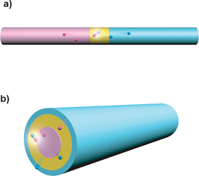 | ||
| Fig. 1 Schematic of carrier generation and separation in (a) axial and (b) radial p-i-n nanowires. The pink, yellow, and blue regions denote the p-type, i-, and n-type diode segments, respectively. The pink and blue spheres denote the holes and electrons, respectively. | ||
A closely related structure is the p-i-n radially-modulated nanowire diode (Fig. 1b). The overall device physics is identical to that of the axially-modulated motif, with the key added benefits being that the p-i-n interface extends along the length of the nanowire and that carrier separation takes place in the radial versus the longer axial direction. Since the latter yields a carrier collection distance smaller or comparable to the minority carrier diffusion length,1,18 photogenerated carriers can reach the p-i-n junction with high efficiency without substantial bulk recombination. Indeed, recent theoretical studies have suggested that coaxial nanowire structures could improve carrier collection and overall efficiency with respect to comparable single-crystal bulk semiconductors, and especially when relatively low quality materials are used as absorber materials.18,20 Large-scale vertically aligned arrays of coaxial nanowires would enable substantial light absorption along the long-axis of the nanowires, and also afford the benefit of short-range and efficient radial carrier separation. Together, these advantages would orthogonalize the pathways for light absorption and carrier collection,18 thereby eliminating a key limitation of conventional planar solar cells, and reduce device surface reflectance,21 which is not the focus of our work and the current tutorial review.
Work from our group has previously demonstrated the key structural and compositional variations needed to explore the axial and radial PV motifs.11 Specifically, a critical breakthrough in the development of nanowire building blocks began with the demonstration of controlled growth of axial22,23 and radial heterostructures,24,25 where the composition and/or doping was modulated down to the atomic level along or perpendicular to the nanowire axes, respectively. In general, synthesis of nanowires proceeds via nanocluster-catalyzed vapor–liquid–solid (VLS) growth.26 With appropriate selection of nanocluster catalyst diameter, reactant gases, pressure, and temperature, one can effect axial modulation of composition and/or axial growth followed by radial deposition of multiple concentric shells to yield radially-modulated structures (Fig. 2a). It should be noted that effective relaxation of lateral strain in these nanoscale structures can enable high-quality integration of materials with larger lattice mismatches than possible in traditional planar structures.22,27 For example, high-resolution transmission electron microscopy (HRTEM) images and elemental maps of 20 nm diameter axially-modulated gallium arsenide–gallium phosphide (GaAs–GaP) nanowires (Fig. 2b) demonstrate that the nanowires are defect-free despite a nearly 3.9% lattice mismatch.22 Elemental mapping of As and P content (Fig. 2c) further shows that the GaAs and GaP regions are spatially well-defined with a relatively sharp (on the order of 10 nm) interface between the distinct regions.
![Axial and radial nanowire heterostructures. (a) Schematic of controlled synthesis; preferential reactant incorporation at the catalyst (growth end) leads to 1D axial growth. A change in the reactant leads to either axial (upper panel) or radial (lower panel) heterostructure growth depending on whether the reactant is preferentially incorporated at the catalyst or uniformly on the wire surface. (b) HRTEM of a GaAs/GaP junction; inset shows two-dimensional Fourier transform of the image. The dashed yellow line marks the junction interface. (c) Elemental mapping of P (red) and As (blue) content of the junction. (d) HRTEM image of single crystalline n-GaN/InGaN/p-GaN nanowire taken along the [0001] zone axis. The inset shows the corresponding electron diffraction pattern. Dashed yellow lines mark the junction interfaces. (e) Normalized EDX line profiles for gallium (blue symbols) and indium (red symbols). Insets: scanning TEM image of the nanowire, and model for the nanowire cross-section (blue and red regions represent GaN and InGaN, respectively). Adapted from ref. 22 and ref. 25.](/image/article/2009/CS/b718703n/b718703n-f2.gif) | ||
| Fig. 2 Axial and radial nanowire heterostructures. (a) Schematic of controlled synthesis; preferential reactant incorporation at the catalyst (growth end) leads to 1D axial growth. A change in the reactant leads to either axial (upper panel) or radial (lower panel) heterostructure growth depending on whether the reactant is preferentially incorporated at the catalyst or uniformly on the wire surface. (b) HRTEM of a GaAs/GaP junction; inset shows two-dimensional Fourier transform of the image. The dashed yellow line marks the junction interface. (c) Elemental mapping of P (red) and As (blue) content of the junction. (d) HRTEM image of single crystalline n-GaN/InGaN/p-GaN nanowire taken along the [0001] zone axis. The inset shows the corresponding electron diffraction pattern. Dashed yellow lines mark the junction interfaces. (e) Normalized EDX line profiles for gallium (blue symbols) and indium (red symbols). Insets: scanning TEM image of the nanowire, and model for the nanowire cross-section (blue and red regions represent GaN and InGaN, respectively). Adapted from ref. 22 and ref. 25. | ||
An illustrative example of a sophisticated radially-modulated nanowire heterostructure relevant to the PV motif is that of n-doped gallium nitride/indium gallium nitride/p-doped gallium nitride (n-GaN/InGaN/p-GaN), where the n-GaN is the nanowire core produced by axial VLS elongation, and the InGaN and p-GaN are shells grown in sequential radial growth steps.25 The HRTEM image (Fig. 2d) and elemental mapping (Fig. 2e) verify the exquisite level of synthetic control possible even in such complicated nanowires. Specifically, HRTEM analysis confirms that the core-shell structure is single crystalline with no interfacial defects, and elemental maps confirm the uniform distribution and expected profile of Ga and In elements.
The above representative examples of axially- and radially-modulated structures highlight several key points of importance to the development of these modulated nanowire motifs for PV applications. First, single-crystalline materials with low defect densities, as demonstrated in the structures of Fig. 2, are beneficial for PV applications because defects can function as deleterious recombination centers that reduce open circuit voltages and short-circuit currents.18,19 Second, it is necessary to have synthetic control over the material band gap, morphology and dimensions of key diode segments to enable tuning of parameters such as absorption depth and depletion region width/length, and to make possible the exploration of more sophisticated tandem or quantum-well structures.1,4,8,9 Third, well-controlled n-type and p-type doping is required to tune the built-in potential at the diode junction interfaces,19 to reduce traps, and to ensure reliable ohmic contacts.
Together, the aforementioned points motivated our decision to use silicon nanowire heterostructures with diameters of at least 200 nm for PV study. The choice of silicon reflects the fact that this material has enabled synthesis of nanowires with control of doping, morphology (e.g. single-crystal, nanocrystal, amorphous) and contacts, and thus allows for clear study of fundamental parameters influencing the nanowire PV elements. Furthermore, the compatibility of silicon nanowire device processing with well-established microelectronics industry protocols presents a unique advantage for integration of these nanoscale PV elements within existing and future electronics. Finally, the ability to prepare high-quality axial and radial Si p-i-n junctions should enable systematic investigation of the limits/advantages of nanowire structures in general for solar energy conversion.
Both axial and radial p-i-n Si-nanowires are synthesized via the gold-nanoparticle catalyzed VLS growth method,11–13,24,26 using silane (SiH4), diborane (B2H6) and phosphine (PH3) as silicon source, and p-type and n-type dopants, respectively, and guided by the Au–Si phase diagram (Fig. 3a). A typical VLS process (pink region) starts with the dissolution and saturation of gaseous reactants into nanosized liquid droplets of a catalyst metal (e.g.Au), followed by nucleation and growth of single-crystalline nanowires. The phase diagram shows that silicon nanowire axial growth (pink region) is preferred at lower temperatures (~400–500 °C) and higher SiH4 partial pressures, while radial growth (blue region) occurs preferentially at higher temperatures (~600–800 °C) and lower SiH4 partial pressures.
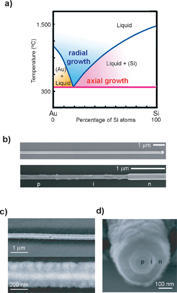 | ||
| Fig. 3 (a) Binary phase diagram for Au and Si illustrating the thermodynamics of axial and radial nanowire growth. (b) SEM images of p-i-n axial Si-nanowire before (upper panel) and after (lower panel) wet-chemical etching. (c) SEM images of the p-i-n coaxial Si-nanowire at two different magnifications. (d) Cross-section SEM image of a coaxial Si-nanowire after wet-chemical etching from the cleaved end. Adapted from ref. 12 and 13. | ||
For axial p-i-n silicon nanowires, dopant modulation is achieved by switching dopant precursor gases at appropriate times during nanowire elongation.28,29Field-emission scanning electron microscopy (SEM) images indicate that the as-grown axial p-i-n Si-nanowires are straight, have smooth surfaces, and a uniform diameter with <1% deviation along the typical 25 μm length (Fig. 3b, top). Independently calibrated growth rates for each segment of Si-nanowire growth obtained on homogeneous p-, i-, and n-type Si-nanowires prepared under similar conditions have shown that the lengths of the Si-nanowires are consistent with overall growth times.13 In addition, the uniform diameters demonstrate that axial growth is the predominant process under these experimental conditions. In order to verify successful encoding of designed p-i-n structures, the Si-nanowires were selectively-etched in potassium hydroxide solution, where the single-crystal Si-nanowire radial etching rate, R, goes as Ri > Rp > Rn. SEM images of etched p-i-n Si-nanowire structures (Fig. 3b bottom) show clear delineation of the individual regions of the diode structure, which can be referenced to the Au nanocluster catalyst at the end of the last (n-type) segment.13 Finally, the Si-nanowire etching profile follows the order in which dopants were introduced during synthesis: first boron for p-type, no dopant for i-type, and then phosphorus for n-type.
For the radial structure, p-core growth proceeds as for the axial case and is followed by deposition of i- and n-shells at higher temperature and lower pressure to inhibit axial elongation of the Si-nanowire core during the radial growth.12SEM images of a typical p-i-n coaxial Si-nanowire recorded in the back scattered electron imaging mode (Fig. 3c) highlight several key features. First, the uniform contrast of the nanowire core is consistent with a single-crystalline structure expected for Si-nanowires obtained by the VLS method.26 Second, contrast variation observed in the shells is indicative of a polycrystalline structure with grain size on the order of 30–80 nm. HRTEM images confirm that the nanowire shells are indeed polycrystalline. We note here and later comment in greater detail, that this nanocrystalline shell structure may enhance light absorption by the nanowires. In analogy with the etching technique used to delineate the axial p-i-n diode regions, an SEM image of the cross-section of a radial p-i-n Si-nanowire (Fig. 3d) clearly reveals the distinct p-core and i- and n-shell portions of the structure. Together, these observations show that our designed synthesis can reliably yield axial and radial p-i-n Si-nanowires with controlled encoding of the length (thickness), dopant profile, and material morphology within different regions. Control of these parameters is, of course, the prerequisite for producing well-defined diode structures necessary for investigating PV devices.
The electrical transport properties of the axial and radial p-i-n Si-nanowire devices have also been characterized by current–voltage (I–V) measurements under dark conditions at room temperature. Dark I–V characteristics recorded from axial p-i-n devices with i-region lengths of 0, 2 and 4 μm are shown in Fig. 4a.13 Overall, these data show well-defined current rectification, which is characteristic of the diode structure, and a current onset in forward bias at ca. 0.6 V. The onset value is typical for a p-nsilicon diode with the built-in potential being established as the difference between the Fermi energies in the p- and n-type regions.19I–V curves recorded across the p- or n- segments alone in p-i-n Si-nanowire devices containing multiple contacts (upper inset, Fig. 4a) showed linear behavior (lower inset, Fig. 4b), thus confirming that the contacts are ohmic to the p- and n-type segments, and that current rectification is due solely to the built-in electric field across the p-n or p-i-n junction. We also note that the reverse bias leakage current (V < −1 V) is largest for the p-n Si-nanowire diodes. This leakage can be attributed to larger interfacial recombination in the p-n diodes that is reduced with inclusion of an i-region in the p-i-n Si-nanowires.
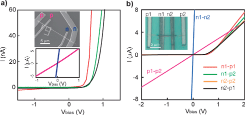 | ||
| Fig. 4 Dark I–V characteristics of p-i-n Si-nanowire devices. (a) Data recorded from axial p-i-n Si-nanowire devices with different i-region lengths; red, green, and black curves correspond to i-segment lengths of 0, 2 and 4 μm, respectively. Upper inset: SEM image of p-i-n Si-nanowire device with i-length of 2 μm, p- (pink) and n- (dark blue) contacts marked. Lower inset: I–V curves recorded from two p- (pink) and n- (dark blue) contacts. (b) I–V curves from coaxial p-i-n device. Inset: optical microscope image of the device. Adapted from ref. 12 and 13. | ||
Dark I–V curves obtained from radial p-i-n devices (Fig. 4b) likewise exhibit characteristics indicative of formation of good diodes.12 Linear I–V curves from core–core (p1–p2) and shell–shell (n1–n2) configurations demonstrate that ohmic contacts are made to both core and shell portions of the nanowires, with the latter showing higher conductance versus the core. Significantly, the highly conductive n-shell will reduce or eliminate potential drop along the shell, thereby enabling uniform radial carrier separation and collection when illuminated.12,18I–V curves recorded from different core-shell contact geometries show rectifying behavior, and demonstrate that the p-i-n radial Si-nanowires behave as well-defined diodes.
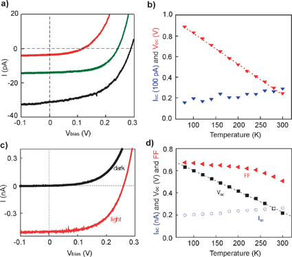
The photovoltaic properties of the axial and radial p-i-n Si-nanowire diodes were characterized under standard conditions of 1-sun (100 mW cm−2) AM 1.5 G illumination. Representative light I–V data for p-n, p-i-n i = 2 μm, and p-i-n i = 4 μm devices (Fig. 5a) yield open-circuit voltage, Voc, and short-circuit current, Isc, values of 0.12 V and 3.5 pA, 0.24 V and 14.0 pA, and 0.29 V and 31.1 pA, respectively. The results reveal a systematic improvement in both Voc and Isc with increasing i-segment length with the largest increase in Voc observed in moving from the p-n to p-i-n structural motif. Qualitatively, the improvement of Voc is consistent with the reduction of leakage currents upon inclusion of the i-segment. Likewise, the systematic increase in Isc as a function of increasing i-segment length is consistent with previous studies of Si-nanowire avalanche photodiodes29 which identified the intrinsic region as the most optically sensitive device region. The fill-factor, FF, for the i = 4 μm device is 51% and yields a maximum power output per nanowire of 4.6 pW. This value is approximately 15 times smaller than that achievable at 1-sun illumination using radial p-i-n Si-nanowire devices,12 (see below) but is still ca. 1000 times larger than that achieved with single piezoelectric nanowires.30 In addition, the estimated AM 1.5 G efficiency, η, based on the projected active area of the i = 4 μm device is 0.5%, which is similar to the 0.46% value reported for single Si-nanowires with metal/semiconductor junctions,31 but considerably smaller than the 3.4% achieved in radial Si-nanowire devices.12 The apparent short circuit current density (Jsc) calculated based on the projected active area12 is ~3.5 mA cm−2 (Fig. 6a), slightly smaller than that reported for rectifying single metal/Si-nanowire photovoltaic devices (~5.0 mA cm−2), although the nanowire diameter in the latter was 4× larger, ~1 μm.31
 | ||
| Fig. 5 (a) Light I–V curves recorded from axial p-i-n Si-nanowire, i-length = 0 (red), 2 (green), and 4 (black) μm devices with illumination intensity of 100 mW cm−2, AM 1.5 G. (b) Plots of Voc (red) and Isc (blue) vs. temperature for a p-i-n (i = 4 μm) device. (c) Dark and light I–V curves of a coaxial Si-nanowire device. (d) Temperature-dependent data from a coaxial device, where the red triangles, black squares and blue circles correspond to FF, Voc and Isc, respectively. Adapted from ref. 12 and 13. | ||
 | ||
| Fig. 6 (a) Current density vs. voltage for single Si-nanowire coaxial p-i-n (red), axial p-i-n (blue) and Schottky junction (black squares) photovoltaic devices. (b) Device-length-dependent Isc and Jsc (upper bound) plots of coaxial p-i-n Si-nanowire devices. Adapted from ref. 12, 13 and 31. | ||
The axial p-i-n Si-nanowire photovoltaic devices were further characterized by measurement of temperature dependent device photovoltaic characteristics. Voc and Isc data for a p-i-n (i = 4 μm) Si-nanowire device are shown in Fig. 5b.13Voc exhibited a well-defined linear dependence on temperature with a slope of −2.97 mV K−1. Extrapolation of Voc to the 0 K limit yielded a value of 1.12 V that is in agreement with the band-gap of single crystalline silicon.19 In addition, Isc was found to increase weakly with temperature due to a decrease in band-gap with increasing temperature.32–34 These low temperature data further confirm that insertion of the i-segment is critical to improving the junction quality. Further insight into the role that junctions and interfaces play in controlling device performance was obtained through Isc and Voc data for p-n and p-i-n axial devices recorded with illumination intensities from ~0.1 to 6 suns. Significantly, analyses of these data13,33,34 yielded ideality factors n = 1.78 and 1.28, and saturation currents, I0 = 102 and 6.14 fA, for the p-n and p-i-n Si-nanowire diodes, respectively. These results show that introduction of the i-region dramatically reduces the saturation current, and thus a large component of the leakage current in the diode. Lower leakage current improves the quality of the diode, which is reflected in the lower value of n, and leads to the observed larger Voc due to reduced shunt losses (large parallel resistances) at the junction.
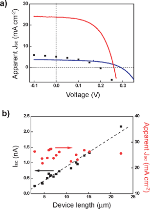
The PV properties of the p-i-n radial Si-nanowire diodes were characterized under identical conditions.12I–V data recorded from one of the better devices (Fig. 5c) yielded a Voc of 0.260 V, Isc of 0.503 nA, and FF of 55.0%. The maximum power output (Pmax) for the Si-nanowire device at 1-sun is ~72 pW, approximately 15 times larger than for the axial p-i-n structure.13 Notably, I–V data recorded on a single Si-nanowire from two devices with p-core to n-shell contact distances of 5.9 and 13.3 μm exhibited the same PV response, indicating that the n-shell is equipotential with radial carrier separation occurring uniformly along the entire length of the radial Si-nanowire.12 The apparent Jsc (Fig. 6a) calculated using the projected area of the radial nanowire structure is 23.9 ± 1.2 mA cm−2.12 The large Jsc in the radial nanowire device implies substantial absorption across the solar spectrum and efficient carrier collection. Such absorption is consistent with the nanocrystalline shell structure of the nanowires and previous studies of polycrystalline thin films,34 although the detailed nature of the absorption will require further investigation. Finally, the apparent PV η of this device was 3.4 ± 0.2%.
In addition, the temperature dependence of Isc, Voc and FF were characterized to understand better the behavior of the radial Si-nanowire PV devices (Fig. 5d).12 Consistent with the observations in the axial structure, Isc increases slightly with increasing temperature, as expected for increased light absorption due to decreasing band-gap with elevated temperature.32 Second, Voc exhibits a substantial linear increase with decreasing temperature, where the slope (dVoc/dT) of −1.9 mV K−1 is close to the value (−1.7 mV K−1) calculated in single crystalline Si solar cells.33 Interestingly, Voc does not extrapolate to the single-crystal Si band gap as expected for a structure consisting of a single-crystal core and polycrystalline shells. The observed increase in Voc can be attributed to a reduced recombination rate at lower temperature,32–34 implying that Si-nanowire photovoltaic performance could be substantially improved at room temperature by reducing recombination processes.34
In Fig. 6a we compare the Jsc/V curves for our previously described axial13 (blue) and radial12 (red) p-i-n Si-nanowire devices in addition to a single unintentionally doped Si-nanowire with diffused metal contacts which form a Schottky barrier device (black).31 It is evident that the single-crystal core/nanocrystalline shell radial device yields Jsc ~ 5× higher than for the single-crystal axial and Schottky devices. As mentioned before, the large measured photocurrents in the former are a consequence of substantial absorption of the solar spectrum by the nanocrystalline silicon material34 and the efficient charge separation in the radial junction.18 We note that while Jsc is roughly constant for devices, the Isc scales linearly with the device length (Fig. 6b) and linearly with device intrinsic segment length for radial and axial devices, respectively. Such scaling identifies a convenient route towards increasing PV performance and, specifically, power output.
Finally, we stress that our radial Si-nanowire devices12 exhibit large short circuit current densities, ~24 mA cm−2, that are comparable to the 24.4 mA cm−2 value for the best thin film nanocrystalline Si solar cell,35 and substantially better than values reported for CdSe nanorod/poly-3-hexathiophene15 and dye sensitized ZnO nanorod16,17 solar cells. Moreover, both axial and radial Si-nanowire devices yield stable improvements in their efficiency with increasing illumination intensity (up to 8 suns measured) and have shown viabilities of up to 14 months without degradation of PV performance. This stresses the ability of all-inorganic p-i-n Si-nanowire PV elements to function as robust power sources in contrast to other nanostructured hybrid inorganic/organic solar cells which often exhibit degradation.15–17
With regards to Voc, there remains significant room for improvement since open circuit voltages in Si-nanowire p-i-n devices are currently in the 0.2–0.3 V range (Fig. 6a) at room-temperature, while conventional single and polycrystalline silicon planar devices show Voc values typically from 0.6–0.7 V.34 It is interesting to note the similar Voc values despite the very different Si-nanowire diode junction geometries and Si-nanowire diameters (axial and radial: 200–400 nm; Schottky: ~1 μm). This is most striking with regards to the p-i-n axial vs. radial Si-nanowire devices whose junction areas differ by a factor of ~50–200 while their Voc values differ by only 10%. We recall the much higher saturation current (I0 = 3.24 pA) for a radial p-i-n Si-nanowire device versus the axial p-i-n Si-nanowire device (I0 = 6.14 fA). Significantly, while this ~103-fold difference reflects much greater interfacial recombination in the former, the resultant effect on Voc is clearly not dominant. Rather, the similarity in Voc suggests that the same physical phenomena (e.g., strong surface recombination) may be responsible for suppressing the absolute Voc in both the axial and radial PV devices. Studies that identify and address the origin of the lower Voc values in both junction architectures, for example, through systematic synthetic variations in junction structure and surface passivation, are currently in progress.
Novel devices and applications
Beyond addressing fundamental questions regarding the performance and limitations of our current axial and radial nanowire PV devices, we are exploring more novel nanoscale PV enabled through highly-controlled nanowire synthesis. Specifically, Fig. 7 illustrates tandem and multiple quantum well (MQW) structures that are natural extensions of the single axial or radial Si-nanowire PV elements. Multiple diodes or cells can be integrated in series in the axial or radial direction during nanowire synthesis to yield tandem structures shown schematically in Fig. 7a. In planar tandem-cells,4,8,34 the constituent units frequently contain different semiconductors stacked in descending order of band-gap to assist in light harvesting. Our approach is to integrate at high density, on a single nanowire, multiple p-i-n diodes to show in principle that voltage and output power can be scaled. In our Si-nanowire heterostructures, we can readily create such tandem devices through axial or radial extension of multiple series diodes and with appropriate modulation of dopant concentration.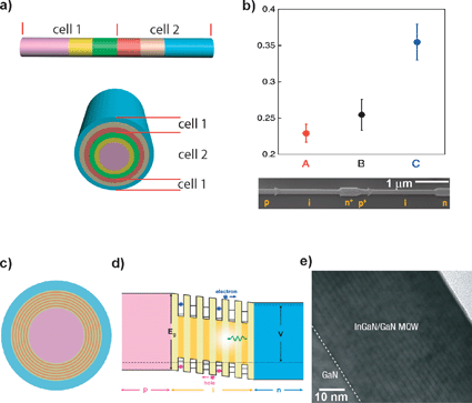 | ||
| Fig. 7 New nanowire structures to improve energy conversion efficiency. (a) Schematics of axial and coaxial nanowire tandem solar cells. (b) Upper panel, Voc for p-i(2 μm)-n (red), p-i(4 μm)-n (black), and p-i-n+-p+-i-n, i = 2 μm (blue) axial Si-nanowire devices; lower panel is an SEM image of an etched p-i-n+-p+-i-n, i = 2 μm axial Si-nanowire device. (c) Schematic of an MQW nanowire solar cell. Pink and blue regions denote p-core and n-shell, respectively; yellow and orange regions are barriers and quantum wells in the i-shell, respectively. (d) Band structure and carrier transport schematics of an MQW nanowire solar cell. (e) Bright-field TEM image of a 26 MQW nanowire cross-section. The dashed line indicates the heterointerface between the core and shell. Adapted from ref. 13, 36 and 37. | ||
To this end, we have synthesized Si-nanowires with a p-i-n+-p+-i-n (i = 2 μm) axial modulation.13 Notably, SEM images of selectively etched (using the protocol described above) Si-nanowires prepared in this manner (Fig. 7b, bottom) clearly demonstrate the successful realization of the p-i-n+-p+-i-n axial modulation. The heavily doped n+ and p+ regions are readily identifiable because of their positions in the tandem device, reduced degree of etching, and expected lengths (~0.5 μm). These results once again confirm that a bottom-up approach can be extended to create structures of substantial complexity, and in this case reliably yield the desired tandem junction sequence with excellent control over the length of the doped regions. Analyses from measurements made on a number of devices13 (Fig. 7b, top) show that the mean Voc for p-i-n+-p+-i-n (i = 2 μm) PV devices, 0.36 (blue) has increased 57% over the value for p-i-n (i = 2 μm) and 39% over p-i-n (i = 4 μm) devices. The power output of the tandem device is 3.2 pW as compared to 2.3 pW for the p-i-n (i = 2 μm) single cell, a 39% increase. The smaller than ideal increase in Voc and output power can be attributed to parasitic series resistance at the n+/p+ interface, and thus represents an area for future focus on synergistic synthesis and device measurements.
In addition, precise control over radial dimensions allows us to insert, in principle, MQW structures into the i-region of radial nanowires (Fig. 7c). Quantum well solar cells (QWSC) have been proposed as an option for increasing energy conversion efficiency above the Shockley–Queissier homojunction solar cell limit.36 The principle of operation centers around quantum wells, which act as absorbers of additional photons, thereby raising the short-circuit current and energy conversion efficiency attainable.36 The output voltage of the nanowire QWSC can be designed to be dominated by the wider band gap barrier material, while the short circuit current can be determined by the width and depth of the quantum well (Fig. 7d). Initial efforts in our lab have led to the first synthesis of defect-free InGaN/GaN MQW structures37 (Fig. 7e), and thus we believe that nanowires are well suited to implementing embedded MQW structures using materials which ordinarily could not be easily implemented on planar devices due to issues of large lattice mismatch.8
Finally, we have demonstrated that our novel Si-nanowire PV elements can be readily interfaced with and provide power for nanoelectronics which consume power at the nano-watt scale.12Fig. 8a shows schematically a Si-nanowire radial PV element connected in parallel with a homogenous nanowire field effect transistor (FET) functioning as a nanowire protein sensor. The binding of charged proteins gates the channel of the nanowire FET leading to a change in nanowire resistance and a concomitant change in voltage drop across the nanowire sensor. Therefore, time dependent change in voltage output of the circuit can be used to monitor the binding/unbinding of analytes. For example, a single Si-nanowire PV device, operating under 8-sun illumination was used to drive a Si-nanowire pH sensor38 without additional power sources (Fig. 8b).12 Measurements of the voltage drop across the p-Si-nanowire sensor (connected in parallel with the Si-nanowire PV power source) as a function of time showed reversible increase (decrease) in voltage as the solution pH was decreased (increased). Such changes are consistent with expected changes in resistance of the Si-nanowire with surface charge.38
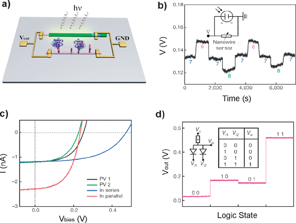 | ||
| Fig. 8 Integrated and self-powered nanosystems. (a) Schematic of self-powered nanowire biosensor. (b) Real-time detection of the voltage drop across a modified silicon nanowire at different pH values. The silicon nanowire pH sensor is powered by a single silicon nanowire photovoltaic device. (c) Light I–V curves (1-sun, AM 1.5 G) of two silicon nanowire photovoltaic devices (PV 1 and PV 2) individually and connected in series and in parallel. (d) Nanowire AND logic gate powered by two silicon nanowire photovoltaic devices in series. Adapted from ref. 12. | ||
Lastly, we demonstrated that multiple integrated Si-nanowire PV elements can drive larger loads, such as nanowire logic gates.12 Two radial Si-nanowire PV devices (black, green) interconnected in series (blue) and in parallel (red) yield Voc and Isc values, respectively, that are nearly the sum of the two constituent devices, as expected (Fig. 8c). Notably, we have used two series interconnected Si-nanowire PV elements as the sole power supply to drive a nanowire-based AND logic gate (Fig. 8d). Measured voltage output levels and a tabulated summary of input/output logic states demonstrated correct AND logic. Notably, such results highlight that even without full optimization, Si-nanowire PV elements can function effectively as integrated power sources in practical nanoelectronic device applications. With proper on-chip scale-up techniques, involving vertical39 and horizontal in-plane40 integration via epitaxial growth and high density printing, respectively, one could realize a nanowire PV enabled solar cell with much larger power output.
Conclusion
We have reviewed some of the initial, critical studies designed to determine the fundamental limits and promises of nanowires as single nanoscale PV solar cells. After close examination of optimized radial and axial p-i-n structural motifs, we have demonstrated measured Jsc values of 24 and 3.5 mA cm−2, respectively, Voc values of 0.26 and 0.29 V, respectively, and efficiencies of 3.4 and 0.5%, respectively. These results already hold great promise in comparison to existing nano-enabled solar cells, however, detailed studies must still be aggressively pursued to understand the physical source of and improve low Voc values in these structures with respect to conventional planar solar cells. Furthermore, building on our controlled design and synthesis of Si-nanowire PV elements with reproducible and carefully tunable PV properties, we have begun to explore increasingly complex and novel nanowire tandem cell and quantum well structures in order to take rational steps towards enhancement of PV efficiency with built-in light trapping structures. More generally, we believe that these and future fundamental studies at the single nanostructure level will be able to illuminate the key intrinsic properties, which if addressed could yield breakthroughs in efficiency, such that nano-enabled PVs might truly lead to a new generation of solar cells capable of providing economical power on a large scale.References
- N. S. Lewis, Science, 2007, 315, 798–801 CrossRef CAS.
- Basic Research Needs for Solar Energy Utilization, Report of the Basic Energy Sciences Workshop on Solar Energy Utilization. April 18–21, 2005, US Department of Energy, Washington, DC, 2005 (http://www.er.doe.gov/bes/reports/abstracts.html#SEU) Search PubMed.
- Form EIA-63B, Annual Photovoltaic Module/Cell Manufacturers Survey, Energy Information Administration, United States, 2006 Search PubMed.
- D. Ginley, M. A. Green and R. Collins, MRS Bull., 2008, 33, 355–364 CAS.
- S. E. Shaheen, D. S. Ginley and G. E. Jabbour, MRS Bull., 2005, 30, 10–19 CAS.
- M. Graetzel, MRS Bull., 2005, 30, 23–27 CAS.
- C. J. Brabec, J. A. Hauch, P. Schilinsky and C. Waldauf, MRS Bull., 2005, 30, 50–52.
- F. Dimroth and S. Kurtz, MRS Bull., 2007, 32, 230–235 CAS.
- R. R. King, D. C. Law, K. M. Edmondson, C. M. Fetzer, G. S. Kinsey, H. Yoon, R. A. Sherif and N. H. Karam, Appl. Phys. Lett., 2007, 90, 183516 CrossRef : 1–3.
- A. Luque, A. Marti and A. J. Nozik, MRS Bull., 2007, 32, 236–241.
- Y. Li, F. Qian, J. Xiang and C. M. Lieber, Mater. Today (Oxford, UK), 2006, 9, 18–27 CrossRef CAS.
- B. Tian, X. Zheng, T. J. Kempa, Y. Fang, N. Yu, G. Yu, J. Huang and C. M. Lieber, Nature, 2007, 449, 885–890 CrossRef CAS.
- T. J. Kempa, B. Tian, D. Kim, J. Hu, X. Zheng and C. M. Lieber, Nano Lett., 2008, 8, 3456–3460 CrossRef CAS.
- M. Graetzel, Nature, 2001, 414, 338–344 CrossRef CAS.
- W. U. Huynh, J. J. Dittmer and A. P. Alivisatos, Science, 2002, 295, 2425–2427 CrossRef CAS.
- M. Law, L. E. Greene, J. C. Johnson, R. Saykally and P. Yang, Nat. Mater., 2005, 4, 455–459 CrossRef CAS.
- J. B. Baxter and E. S. Aydil, Appl. Phys. Lett., 2005, 86, 053114 CrossRef : 1–3.
- B. M. Kayes, H. A. Atwater and N. S. Lewis, J. Appl. Phys., 2005, 97, 114302 CrossRef : 1–11.
- S. M. Sze, Physics of Semiconductor Devices, John Wiley & Sons, New York, NY, 2nd edn, 2004 Search PubMed.
- Y. Zhang, L. W. Wang and A. Mascarenhas, Nano Lett., 2007, 7, 1264–1269 CrossRef CAS.
- L. Hu and G. Chen, Nano Lett., 2007, 7, 3249–3252 CrossRef CAS.
- M. Gudiksen, L. J. Lauhon, J. Wang, D. Smith and C. M. Lieber, Nature, 2002, 415, 617–620 CrossRef CAS.
- Y. Wu, J. Xiang, C. Yang, W. Lu and C. M. Lieber, Nature, 2004, 430, 61–65 CrossRef CAS.
- L. Lauhon, M. S. Gudiksen, D. Wang and C. M. Lieber, Nature, 2002, 420, 57–61 CrossRef CAS.
- F. Qian, Y. Li, S. Gradecak, D. Wang, C. J. Barrelet and C. M. Lieber, Nano Lett., 2004, 4, 1975–1979 CrossRef CAS.
- A. Morales and C. M. Lieber, Science, 1998, 279, 208–211 CrossRef CAS.
- M. T. Bjork, B. J. Ohlsson, T. Sass, A. I. Persson, C. Thelander, M. H. Magnusson, K. Deppert, L. R. Wallenberg and L. Samuelson, Appl. Phys. Lett., 2002, 80, 1058–1060 CrossRef CAS.
- C. Yang, Z. Zhong and C. M. Lieber, Science, 2005, 310, 1304–1307 CrossRef CAS.
- C. Yang, C. J. Barrelet, F. Capasso and C. M. Lieber, Nano Lett., 2006, 6, 2929–2934 CrossRef CAS.
- Z. L. Wang and J. Song, Science, 2006, 312, 242–246 CrossRef CAS.
- M. D. Kelzenberg, D. B. Turner-Evans, B. M. Kayes, M. A. Filler, M. C. Putnam, N. S. Lewis and H. A. Atwater, Nano Lett., 2008, 8, 710–714 CrossRef CAS.
- M. A. Green, Prog. Photovolt: Res. Appl., 2003, 11, 333–340 CrossRef CAS.
- P. Würfel, Physics of Solar Cells, From Principles to New Concepts, Wiley-VCH Verlag GmbH & Co. KGaA, Weinheim, 2005 Search PubMed.
- A. Luque and S. Hegedus, Handbook of Photovoltaic Science and Engineering, Wiley, Chichester, 2003 Search PubMed.
- M. A. Green, K. Emery, D. L. King, Y. Hishikawa and W. Warta, Prog. Photovolt: Res. Appl., 2008, 16, 61–67 CrossRef.
- K. W. J. Barnham and G. Duggan, J. Appl. Phys., 1990, 67, 3490–3493 CrossRef CAS.
- F. Qian, Y. Li, S. Gradecak, H. -G. Park, Y. Dong, Y. Ding, Z. L. Wang and C. M. Lieber, Nat. Mater., 2008, 7, 701–706 CrossRef CAS.
- Y. Cui, Q. Wei, H. K. Park and C. M. Lieber, Science, 2001, 293, 1289–1292 CrossRef CAS.
- J. M. Spurgeon, K. E. Plass, B. M. Kayes, B. S. Brunschwig, H. A. Atwater and N. S. Lewis, Appl. Phys. Lett., 2008, 93, 032112 CrossRef : 1–3.
- A. Javey, S. Nam, R. S. Friedman, H. Yan and C. M. Lieber, Nano Lett., 2007, 7, 773–777 CrossRef CAS.
Footnote |
| † Part of the renewable energy theme issue. |
| This journal is © The Royal Society of Chemistry 2009 |