Polymeric and biomacromolecular brush nanostructures: progress in synthesis, patterning and characterization
Robert
Ducker
,
Andres
Garcia
,
Jianming
Zhang
,
Tao
Chen
and
Stefan
Zauscher
*
Center for Biologically Inspired Materials and Material Systems, Pratt School of Engineering, Duke University, Durham, NC, USA. E-mail: zauscher@duke.edu
First published on 18th July 2008
Abstract
A significant scientific and engineering challenge of recent years has been the fabrication of patterned polymeric and biomacromolecular brush nanostructures on surfaces. These structures provide researchers with a rich platform on which to exploit and observe nanoscale phenomena. In this review we present an overview of the field and highlight, through selected examples, recent advances in the nanostructuring of polymer and biomacromolecular brushes. This includes a brief overview of polymer brush synthesis techniques and how these are integrated with nanolithographic and templating approaches. We discuss the characterization of polymeric nanostructures and its associated difficulties, and we provide some perspective of how we see the future direction of the field evolving.
Dr Robert Ducker is working on research projects in Dr Zauscher’s lab that range from synthesis and surface functionalization of ferroelectric thin films to chemical surface patterning using programmable spatial light modulators. Andres Garcia’s graduate research in Dr Zauscher’s lab centers around the development and implementation of nanolithographic techniques using electric field induced scanning probe lithography. Jianming Zhang is working on the synthesis and characterization of polymeric and biomolecular brush nanostructures. Dr Tao Chen is working on the fabrication, manipulation and characterization of stimulus-responsive biomolecular and bio-inspired polymeric brush nano- and microstructures. |
 Stefan Zauscher | Dr Stefan Zauscher is an associate professor in the Department of Mechanical Engineering and Materials Science at Duke University. Dr Zauscher’s research lies at the intersection of surface and colloid science, polymer materials engineering, and bio-interface science. |
1 Introduction
One central goal of materials science and engineering is to produce hierarchical materials that are ordered over a range of length scales and in which larger scale structural and physico-chemical properties are controlled by molecular characteristics.1 Novel methods for the synthesis and fabrication of nanopatterned or templated polymer and biomolecular brushes, with controlled molecular architecture, chemical functionality, and size, have spawned opportunities for tailoring surface properties by imparting them with desirable energetic, mechanical, biological, optical, and electrical properties.2Polymer brushes are ensembles of polymer chains that are tethered with one end to and densely packed on a surface or interface.3,4 The ensuing lateral conformational restraint leads to steric repulsive interactions between the packed chains and causes the polymer molecules to extend away from the substrate surface.2,3 Such brushes are often confined to patterned, planar substrates that direct and localize the ‘top-down’ or ‘bottom-up’ synthesis of the brush. In addition to planar substrates, nanostructured materials and nanosize materials are used frequently as templates for the fabrication of polymer brushes.Polymers and biomacromolecules can be designed and synthesized to be responsive to changes in their surrounding solvent medium; e.g. brushes can undergo phase transitions with measurable structural and morphological changes upon variations to external stimuli such as temperature, ionic strength and pH value.4 Fabricating such polymeric and biomacromolecular structures on surfaces and the control of their architecture on the nanometre length scale is important for a wide range of applications,5 such as biosensors,6 proteomic chips7 and nanofluidic devices.8
The number of papers in the field has rapidly grown over the last 13 years (Fig. 1). A recent search of the ISI Web of Science produced over 630 returns using ‘nano* AND polymer AND brush*’ as search terms, and produced over 70 returns using ‘polymer AND brush* AND pattern* AND nano*’ as search terms. Here we present an overview of the field and highlight, through select examples, recent advances. This includes a brief overview of polymer brush synthesis techniques and how these are integrated with nanolithographic and templating approaches. We discuss the characterization of polymeric nanostructures and its associated difficulties, and conclude with our view on how the field is developing.
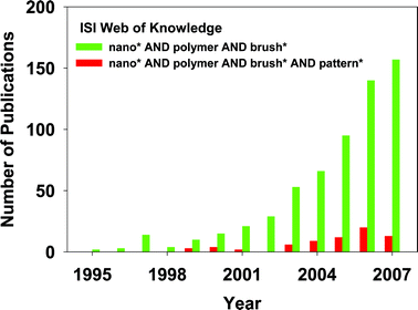 | ||
| Fig. 1 Number of publications per year retrieved by a search of the ISI Web of Knowledge with the search terms “nano* AND polymer AND brush*” and “polymer AND brush* AND pattern* AND nano*”. | ||
2 Polymeric and biomacromolecular brush syntheses
Generally two synthetic approaches are used to synthesize polymer brushes: the grafting-from approach, through surface initiated polymerization (SIP),9,10 which yields polymer brush structures by direct synthesis from the surface, and the grafting-to approach that adheres pre-synthesized polymers or biomacromolecules to a surface.11 A main drawback of the grafting-to method lies in the limited grafting density that can be achieved due to the increasing steric hindrance as the brushes attach to the surface. In SIP, however, the polymer chains are grown from surface-bound initiators, eliminating much of the steric effects that are associated with attaching polymer chains to the surface. When compared with the grafting-to approach, this grafting-from approach provides greater control over grafting density and yields higher packing densities. Self-assembled monolayers (SAMs), such as suitably functionalized alkylchlorosilane12 and alkanethiol13 SAMs, provide reliable initiators for SIP. For an in-depth discussion of SAMs the reader is directed to these reviews.5,14,152.1 SIP of polymer brushes
The seminal work by Prucker and Rühe10,16 led the way for SIP of polymer brushes using free radical polymerization. Although the templated fabrication of polymeric nanostructures from the bottom up has been prototypically demonstrated, and many methods for SIP, including anionic,17 cationic,18 plasma induced,19 condensation,20 photochemical,21 electrochemical,22 and ring-opening metathesis polymerization (ROMP),23 have been used, the preparation of precisely patterned, surface-bound polymeric nanostructures with controlled lengths, conformational geometries, functionalities, and properties, still poses significant challenges and is an active area of research.In particular, controlled radical polymerizations (CRPs) provide versatile approaches for the synthesis of polymer brushes of controlled architecture and height.24,25 For example, atom transfer radical polymerization (ATRP), a transition metal based, CRP chemistry, affords advantages over other synthetic methods,24 because it leads to well-controlled brush growth under mild conditions, with defined molecular weight and low polydispersity and, as a result of the ‘living’ nature of the catalyst, allows the ready synthesis of block copolymers. ATRP is compatible with a variety of functionalized vinyl monomers such as styrene,26 acrylates,27 acrylamides,28 and acrylonitrile.29 Due to the reversible activation/deactivation processes between the radical end of the growing polymer chains and the transition metal based catalysts, the growth rate of polymer brushes can be widely tuned by altering ratio and concentration of reactants and catalysts. Kinetic challenges in the synthesis of short, low molecular weight brushes can be addressed by adding ‘sacrificial initiator’ to the reaction solution.30
2.2 Biomacromolecular brushes
Although many patterning and grafting methods for biomolecules, such as peptides, DNA,31 and proteins,32,33 have emerged recently,15,34 the controlled synthesis of densely packed, biomacromolecular nanostructures is not as developed and subject to significant research efforts. The grafting density and precision with which one can organize large biomolecules (polypeptides and DNA) on surfaces depends largely on the quality and chemical functionality of the affinity template nanostructure,32 and is fundamentally limited by the size exclusion inherent in the currently used grafting-to approaches. This limitation has stimulated research in SIP of biomolecules. Chow et al.31,35 were the first to demonstrate enzymatically assisted SIP of single stranded DNA, from thiolated oligonucleotide initiators of different grafting density patterned onto gold surfaces (Fig. 2). In this approach, a SAM of an oligonucleotide thiol (5′SH-(CH2)6-T25) is deposited onto nanopatterned gold islands. These templates are then amplified by enzymatically catalyzed SIP of mononucleotide using TDtase. This approach yielded polynucleotide brushes with a height of ∼100 nm.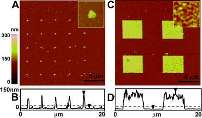 | ||
| Fig. 2 Tapping mode AFM images in air for gold arrays of different feature sizes (A,B: 0.1 μm. C,D: 4 μm) with 5′-SH-(CH2)6-T25 SAM after a 2 h incubation with TdTase. Insets are the images of A and C at a higher magnification. B and D are the line profiles of A and C. Dotted lines represent the average height of gold arrays and immobilized DNA-SAM. Reprinted with permission from ref. 31. Copyright 2005 American Chemical Society. | ||
Another interesting example of growing high aspect ratio, brush-like biopolymers on surfaces was reported by Brough et al.33 In their approach, actin structures were grafted from a biotinylated gelsolin initiator fragment and short F-actin, leading to active actin growing sites. Densely packed micron-sized actin filaments were synthesized by this approach.
3 Patterning of polymer brushes
Optical and electron-beam lithographic (EBL) techniques have a long-standing tradition in the semiconductor industry,36 for patterning substrate surfaces with sub-micrometre features and have been successfully adopted for the templated fabrication of polymeric and biomolecular brushes. More recently, scanning probe lithographic techniques have become popular with researchers, due to their versatility in the fabrication of nanostructures. Finally, inherently nanostructured materials have been used as templates for polymer brush growth.3.1 Photolithography and plasmonic lithography
Photolithography is a convenient and widely used method for fabricating micro- and nanostructures and templates on solid substrates, and generally involves the exposure and subsequent selective removal of a polymeric photoresist.37,38Photolithography can often be a simple and flexible tool to pattern micrometre and sub-micrometre features over large areas.39 The spatial resolution of the technique is largely determined by the Abbe diffraction limit40 (a far-field effect), which limits the feature size to about half the wavelength of the light used. Use of deep UV radiation and technological advancements have afforded features of less than 200 nm.39Prucker et al.41 were among the first to realize the potential in using photolithography to microstructure molecularly thin polymer layers. Photolithography is used in two ways for the fabrication of patterned polymer brushes. In the phototemplating approach a photoresist covered substrate surface can be selectively patterned by exposing the resist through a mask using UV light; the polymer resist in the illuminated areas degrades and is subsequently removed.12 After removing the exposed resist, the substrate can be functionalized with initiator for SIP. Husemann et al.42 combined photolithographic techniques with surface-initiated polymerization to create discrete areas of hydrophilic and hydrophobic polymer brushes. In a more elegant method, demonstrated by Prucker et al.,43 a surface-bound azobis-isobutyronitrile (AIBN) initiator was selectively activated using ‘soft’ UV on the substrate such that polymerization only took place in the illuminated areas. Subsequently a polymer brush was grown by free radical polymerization in these activated areas and not the masked areas, where the initiator remained inactive.
Zhou et al.26 fabricated a binary polymer brush pattern by a two-step surface-initiated ATRP. First, a monolayer of initiator was created and the first polymer brush was synthesized. This brush was passivated and then etched by UV irradiation through a simple shadow mask. A second initiator was then attached to the exposed areas from which the second polymer was grown.
In an effort to increase patterning resolution, interference lithography has been used to create patterned, nanoscale polystyrene brushes over a large surface area.44 In this approach, extreme ultraviolet (EUV) radiation from a synchrotron-based interference setup was used to create initiator radicals on the substrate surface in the interference pattern. During the subsequent polymerization reaction, brushes were only grafted to the sections of the surface that had been exposed to EUV radiation.
Several photolithographic approaches that can circumvent the diffraction limit of light exist but have not yet been used for patterning polymer brushes. One such approach uses a plasmonic lens to fabricate nanoscale structures on surfaces.45 While a conventional lens creates an image by focusing propagating light, a plasmonic lens46 uses surface plasmons to reconstruct sub-diffraction limit ‘information’ that is lost due to the evanescent decay of light. Using plasmonic lithography, 90 nm structures were created with 365 nm light; this corresponds to a feature size of ∼λ/4. This was achieved by fabricating Al plasmonic structures on a quartz substrate, covered with a PMMA resist. The plasmonic structures were then used to expose the photoresist layer. Another, but similar approach is photolithography in the evanescent near-field. This approach has been developed as a static patterning process using a shadow mask in close proximity to a photoresist layer during exposure.47
3.2 Electron beam (chemical) lithography
EBL uses a focused beam of electrons to modify the structure of the substrate surface and can routinely produce structures well below 100 nm, with sub 10 nm resolution being achieved.48 The de Broglie wavelength of electrons in EBL are significantly smaller than those of light in the UV and visible ranges, and enables the patterning of features that are significantly smaller than those accessible by photolithographic techniques. Despite some of the drawbacks of EBL, such as high cost of the instrumentation, the need of ultrahigh vacuum for operation, and the inherently serial patterning, EBL is one of the most powerful techniques to create well-defined features at the nanoscale. Ahn et al.49 used lift-off EBL to fabricate nanoscale gold islands for the templated SIP of stimulus-responsive poly(N-isopropylacrylamide) (pNIPAAM) brushes through ATRP (Fig. 3) and also for the templated synthesis of polynucleotide brushes.31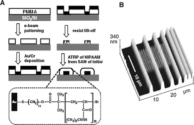 | ||
| Fig. 3 Stepwise fabrication process of surface confined pNIPAAM polymer brush patterns by EBL and SI-ATRP. (B) Tapping mode AFM height image showing micropatterned lines and nanopatterned array of dots. Adapted with permission from ref. 49. Copyright 2004 Wiley-VCH. | ||
Brough et al.33 used EBL for the localized crosslinking of a spin-coated PEG layer, yielding PEG islands with footprint sizes from 50 to 100 nm. Using biotin–streptavidin molecular recognition chemistry, they then immobilized biotinylated gelsolin-based actin initiators on the PEG islands for the subsequent SIP of actin brushes.
Recently, an exciting EBL method has been developed that allows direct control over surface chemistries. In a process termed electron-beam chemical lithography (EBCL), Grunze et al.50,51 fabricated nanopatterns by chemically modifying the end-groups of 4-nitro-1,1′-biphenyl-4-thiol (NBT) SAMs on gold substrates. During EBCL the terminal nitro groups are converted to amine groups while the underlying aromatic layer is dehydrogenated and crosslinked, enhancing its stability. Lines, bearing amine functionality, and having widths ranging from 20 nm to 1 μm were patterned by EBCL. Subsequently, these amine terminated organic nanostructures were used as templates for SIP using a surface-bound ATRP initiator. This approach yielded densely grafted, thermosensitive pNIPAAM brush nanopatterns. Using a similar synthesis approach, sub 50 nm polystyrene brush nanopatterns were fabricated, but in this case, the NBT SAM was first patterned by EBCL followed by diazotization and coupling of methylmalonodinitrile (Fig. 4). This resulted in surfaces with well defined areas of crosslinked initiator sites for PS SIP.52 Steenackers et al.53 found that polymer graft density, and thus brush height, can be finely controlled by adjusting the electron dose during pattern formation. This is shown in Fig. 5a, where the height of the polymer brush asymptotically reaches a maximal height with increasing electron dose; a similar behavior was observed for pNIPAAM brushes.54
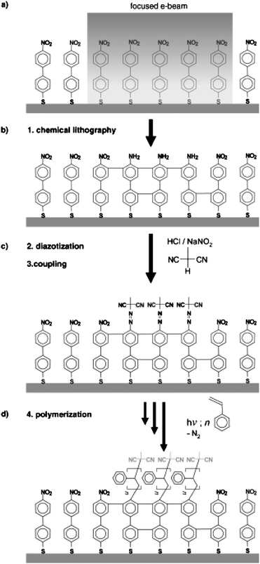 | ||
| Fig. 4 Schematic of the EBCL and SIP process. (A) Irradiation, (B) local conversion, (C) diazotization and coupling, (D) polymerization. Reprinted with permission from ref. 52. Copyright 2007 Wiley-VCH. | ||
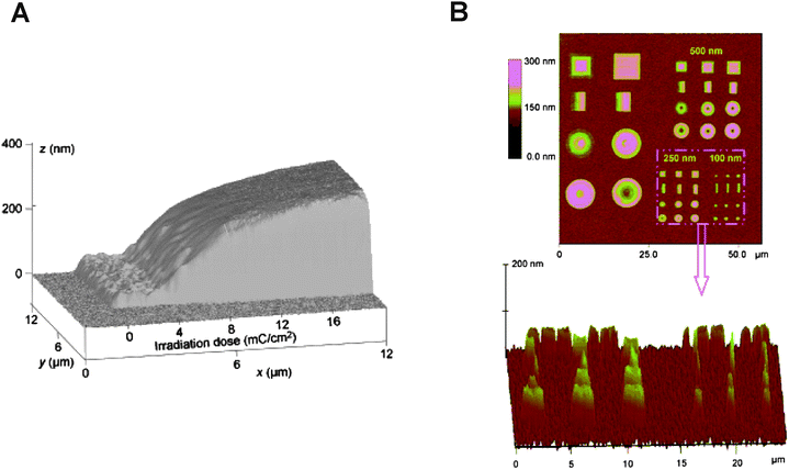 | ||
| Fig. 5 (A) AFM height image showing the brush height gradient as a function of irradiation dose during EBCL. (B) AFM images of pNIPAAM brush patterns showing gradual height variations within some of the patterned features. Adapted with permission from ref. 53,54. Copyright 2007 Wiley-VCH. | ||
In an effort to overcome the need for custom synthesized aromatic SAM resists, Ballav et al.55 used aliphatic dodecanethiol (DDT). After exposure to the electron beam, the patterns were displaced with 11-aminoundecanethiol (AUT). This resulted in amino-terminated AUT templates with a size of ∼50 nm in a background of methyl-terminated DDT. An ATRP bromo-initiator was then attached to the patterned AUT templates for the SIP of pNIPAAM brushes. EBCL has thus opened a new window of opportunities for the creation of polymer brush nanostructures with high resolution and fidelity. EBCL offers the capability to build at both the micro and nanoscale while imparting great control over the grafting density and height of the polymer brushes (Fig. 5b). Furthermore, the chemical modification of SAMs on surfaces provides templates for the fabrication of a wide variety of ‘smart’ polymeric nanostructures.
3.3 Soft lithography
Soft lithography,56 using polymeric stamps for the pattern transfer, was developed by Kumar and Whitesides in the early 1990's.57 It provides a simple and inexpensive method of creating micro- and nanostructures over a large area (0.1–100 cm2).56 An attractive feature of the method is the use of inexpensive polymeric stamps that can be replica molded from suitably patterned masters. In microcontact printing (μCP) a stamp is coated with a chemical species or ‘ink’ that is transferred to a substrate through physical contact. Generally, the feature size and stamping fidelity are determined by the design and the mechanical properties of the polymeric stamp, the diffusivity of the ink, and the contact time and pressure during ink transfer. μCP provides thus a simple and cost-effective method to create micrometre-scale initiator functionalized patterns (silanes on Si/SiO258–60 and thiols on gold61–63) on solid surfaces that can be amplified to create patterned polymer brushes.20,42,64,65Several factors need to be considered, however, when adapting soft lithography for nanoscale printing. The diffusion of low molecular inks (i.e., alkanethiols and silanes) during the printing step can limit resolution. Furthermore, physical limitations also arise when the relief features in the stamp are so small that they are prone to mechanical deformation during ink transfer. The latter problem has been successfully addressed by using a composite stamp that consists of a thin hard PDMS layer supported by a soft, more flexible layer.66 For example, Liet al.67 printed dendrimers and proteins with a feature size of 40 nm directly, using such a stamp. An interesting approach to fabricating patterned multicomponent polymer brushes was shown by Zhou et al.62 who patterned a substrate surface with chemically distinct initiator-terminated thiols in a step and repeat process, without the need of backfilling with an inert alkanethiol (Fig. 6). This approach not only yielded precisely patterned and chemically distinct polymer brushes, but also offered a route to creating polymeric nanostructures in the nanogap between two binary brushes. Nevertheless, to the best of our knowledge, soft lithography has not yet been used to directly print initiators to create nanopatterned polymer brushes.
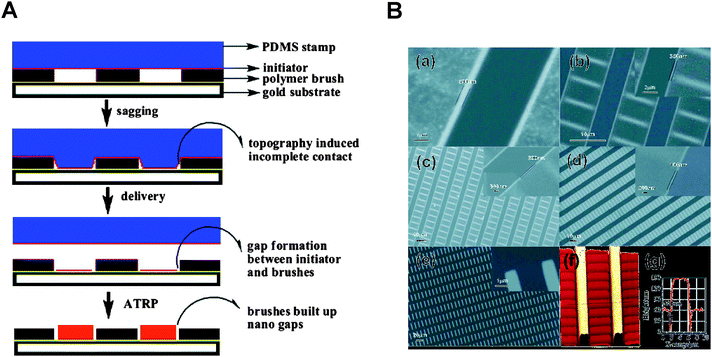 | ||
| Fig. 6 (A) Schematic of nanogap formation due to incomplete stamp contact during micro contact printing. (B) SEM images showing binary polymers and nanogaps. Adapted with permission from ref. 62. Copyright 2006 American Chemical Society. | ||
3.4 Capillary force lithography
Capillary force lithography (CFL) is a simple and robust method that combines aspects of nanoimprint lithography (NIL) and μCP. CFL, like μCP, uses an elastomeric stamp to transfer a pattern with high fidelity and in large scale onto a polymeric thin film but without the need of high pressures, typical for imprint lithography. Once the polymer film is heated above its glass transition temperature, capillary forces cause the softened polymer to fill the open spaces of the elastomeric mold. Liu et al.68 developed a new approach to synthesizing binary, stimulus-responsive polymer brush nanopatterns on a large scale and with high throughput, by combining CFL with SIP. CFL can achieve feature sizes on the order of 100 nm,69 which opens up large-scale patterning on the nanoscale.3.5. Scanning probe lithography
Scanning probe lithography (SPL), using scanning tunneling microscopy (STM),70 or atomic force microscopy (AFM),71 has unique advantages over photolithographic and EBL approaches because of the added capability of these instruments to manipulate and image nanostructures on surfaces. Furthermore, SPL techniques offer a resolution that approaches that of EBL72 but are technologically simpler, significantly cheaper, and therefore more widely accessible to most researchers than EBL or photolithography. SPL provides a broad arsenal of approaches for pattern generation, based on various chemical, physical and electrical modifications of surfaces, including mechanical scratching,73–75 electrochemical anodization of silicon surfaces,76,77decomposition of SAMs,78–81 and electric field induced chemical reactions.82,83 For details we refer to recent comprehensive reviews on SPL.84,85 In the past decade several nanopatterning methods, such as nanoshaving,73anodization lithography86 and ‘dip-pen’ nanolithography (DPN)87 have been employed in the fabrication of nanopatterned polymer brushes as described below. Like with photolithography and EBL, the majority of patterning efforts using SPL has been directed towards fabricating templates for subsequent modification with initiators. A unique feature of many SPL techniques is the intimacy of contact between tip and substrate which provides the ability to deposit initiator directly or to trigger polymerization within a small reaction volume in the meniscus around the scanning probe tip.88Ahn et al.94 used DPN to deposite nanoscale patterns of carboxylic acid terminated SAMs on gold substrates, which served, after conjugation with a free radical initiator, as affinity templates for the SIP of stimulus-responsive pNIPAAM brushes. Kaholek et al.95 succeeded in fabricating stimulus-responsive polymer brush patterns with linewidths of 200 nm, by directly patterning the initiator thiol using DPN, and subsequent amplification of the pattern using ATRP of pNIPAAM in an organometallic catalyst solution.
Liu et al.91 combined dip-pen nanolithography and ring-opening metathesis polymerization (ROMP) to fabricate polymer brush arrays on the nanometre length scale with great control over feature size, periodicity and shape (Fig. 7). In this approach, norbornenylthiol molecules were first patterned onto a gold substrate which was then passivated in a DDT solution and subsequently reacted with Grubbs' first generation catalyst and norbenyl monomers, yielding a polynorbornene brush array with 78 nm feature size.
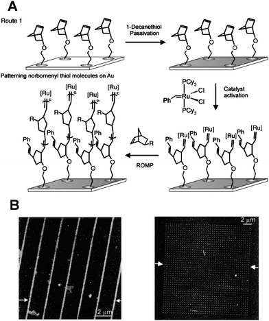 | ||
| Fig. 7 (A) Schematic of surface-initiated ROMP by DPN. (B) Topographic AFM image of polymer brush lines and dot arrays. Adapted with permission from ref. 91. Copyright 2003 Wiley-VCH. | ||
In another approach, surface-bound gold nanostructures were fabricated by DPN and subsequently used as templates for the photoinitiated polymerization of methylmethacrylate (MMA), yielding a lateral resolution of only 20 nm.96 Maynor et al.88 used an electrochemical dip-pen nanolithography (E-DPN)97 to polymerize 3,4-ethylenedioxythiophene (EDOT). This approach yielded conductive poly-EDOT nanostructures with sub 100 nm dimensions on semiconducting and insulating surfaces.
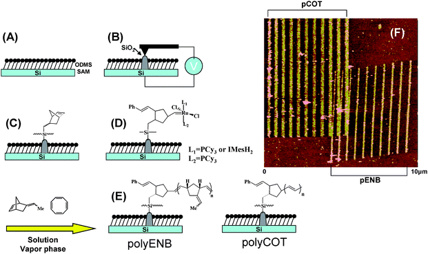 | ||
| Fig. 8 (A)–(E) Schematic for the stepwise fabrication of polymeric nanostructures by surface-initiated ROMP on SiO2 nanopatterns generated by anodization lithography. (F) 10μm × 10μm AFM tapping mode height image of polyCOT and polyENB nanopatterns fabricated by a step-and-repeat process on the same substrate. Adapted with permission from ref. 99. Copyright 2006 Wiley-VCH. | ||
A related technique is apertureless scanning near-field optical microscopy (aSNOM), an extension of the SNOM technique, where large, localized light intensities are achieved by local enhancement of far-field light through a nanometre-sized, pointed probe.104 Although aSNOM offers a significant increase in the optical resolution (∼20 to 50 nm) over other photolithographic approaches, it has the drawback of being a technically demanding technique. Wurtz et al.105 report the photopolymerization of a photoresist induced by near-field enhancement from a sharp probe. This method yielded 70 nm polymeric nanostructures and demonstrated that direct nanopolymerization is possible using near-field techniques. While these photochemical SNOL techniques have not yet been used for the nanoscale patterning and syntheses of polymer brushes on surfaces, it is clear that they provide powerful means to do so.
4 Nanostructured and nanoscale materials for templating
Lithography is not the only approach for the fabrication of polymeric brush nanostructures. Nanostructured materials can provide nanoscale features (templates) that can be used for SIP. Furthermore, nanoscale materials inherently lend themselves as templates for the fabrication of polymeric nanostructures. An example of this is mesoporous silica,16 which can provide templates for the surface initiated synthesis of polymer brushes; e.g., polymer decorated nanopores). Furthermore, inorganic nanoscale materials, such as gold colloids,106 or organic nanoscale materials, such as DNA,107 can function as templates for SIP.4.1 Nanoparticle templates as a lithographic tool
Gold nanoparticles can be used as a shadow mask for the templating of stimulus-responsive polymer brush nanostructures (Fig. 9).108 In this approach, a two-layer polymer resist thin-film was deposited on a glass substrate, using the Langmuir-Blodgett technique. The resist was then covered with Au nanoparticles (∼30 nm diameter), whereby the negatively charged nanoparticles attach to the positively charged polymer. The exposed polymer was etched using UV/O3, leaving the polymer under the nanoparticles protected. These exposed areas were then backfilled with chlorosilane initiator and stimulus-responsive pNIPAAM brushes were grown viaATRP.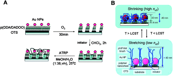 | ||
| Fig. 9 (A) Schematic illustrating (i) the use of Au NPs as shadow masks for surface nanopatterning and (ii) subsequent brush SIP. (B) Schematic illustration of stimulus-responsive polymer brush Au NP hybrid assemblies. Adapted with permission from ref. 108. Copyright 2007 American Chemical Society. | ||
4.2 Polymer brushes on nanostructures
Much of the work on nanoscale patterning of polymers has been involved with fabricating patterns on planar surfaces; yet, apart from arrays, real applications for these types of structures are limited. Nanostructured materials with non-planar surfaces or nanoparticles provide many new directions for possible applications.109 A fundamental problem of working with nanoparticles, however, is stabilizing them in solution while retaining functionality. While this is often done with SAMs or surfactants, polymer brushes are also used, especially to add specific chemical functionality to these systems.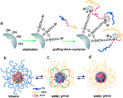 | ||
| Fig. 10 Schematic showing (A) the fabrication of mixed copolymer brushes on the surface of silica nanoparticles, (B) different morphologies of the coating as a function of the solvent type: collapsed P2VP, and stretched PS chains in toluene (a good solvent for PS, and a poor solvent for P2VP), (C) collapsed PS and stretched P2VP, PEO in water at pH < 4 (a good solvent for P2VP and PEO, and a poor solvent for PS), and d) collapsed P2VP, PS and stretched PEO chains in water at pH > 4 (a good solvent for PEO, a poor solvent for P2VP and PS). Reprinted with permission from ref. 110. Copyright 2007 Wiley-VCH. | ||
Silica nanoparticles have also been used as scaffolds to synthesize hollow, polymer brush spheres.111 In this approach, a monolayer of 3-ethyl-3-(methacryloloxy)methyloxetane (EMO) was amplified on the silica nanoparticle into a pEMO brush. A second brush, poly(methylmethacrylate) (pMMA), was then grown by ATRP, to form a pEMO-pMMA diblock copolymer. After crosslinking the pEMO, the silica particle was dissolved, leaving behind a nanoscale cavity, defined by the size of the silica particle and the thickness of the pEMO brush. Such polymeric vesicles have potential applications as a drug delivery system. Another template system used silver nanoparticles, decorated with an amphiphilic, branched polymer brush (PSx-PEOy), that self-assemble into 1-dimensional tubular structures (Fig. 11A,B).112 Khanal and Zubarev,113 took this concept further, and coated gold nanorods with PS polymer brushes and then assembled these nanorods, through the evaporation of solvent, into ring structures (Fig. 11C).
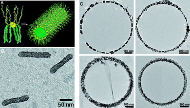 | ||
| Fig. 11 (A) Schematic representation of the amphiphilicity-driven self-assembly of Au-(PS-PEO)n NPs. (B) TEM image of a sample prepared from an aqueous solution of Au-(PS-PEO)n NPs. (C) TEM images of rings formed by AuNR(PS)n rods from a solution in CH2Cl2. Adapted with permission from ref. 112 (Copyright 2006 American Chemical Society) and 113 (Copyright 2007 Wiley-VCH). | ||
Not only nanoparticles, but also nanostructured substrates provide exciting possibilities for templated polymer brush synthesis. For example, one application for stimulus-responsive polymer brushes is that of a molecular gate,114 where conformational changes of the polymer brush are used to control the flow through a nanoporous material. In an interesting approach, poly(glutamic acid) brushes have been used as gates to control the permeation of water through a gold coated, porous membrane.115 Here the gating was achieved by exploiting the conformational change of the brush into a helical structure, when exposed to acidic conditions. More recently, Motornov et al.116 showed that mixed PDMS-P2 VP brushes provide even better pH responsive gating than homopolymer brushes alone.
Carbon nanotubes (CNTs) have attracted a great deal of interest in recent years, due to their excellent electronic and mechanical properties. One major drawback of CNTs is, however, that they are not inherently soluble in water, which also limits their biological applications. This limitation is one of the driving forces behind the functionalization of CNTs with polymer brushes. The functionalization of the surface of multiwalled carbon nanotubes (MWCNTs) with polymers such as pMMA117 and pNIPAAM,118 grown by SI-ATRP, and also with branched and linear biocompatible glycopolymers119 has been reported. Single-walled CNTs have also been decorated with pMMA.120
Recently Pei et al.121 successfully created a CNT–polymer–metal hybrid material. This hybrid material was fabricated by first using a reversible addition and fragmentation chain transfer (RAFT) polymerization to graft a poly(2-hydroxyethyl methacrylate) (pHEMA) polymer brush to the CNT surface. The pHEMA brush was then hydrolyzed to form a pMMA brush, which was subsequently used to chelate Ag+ ions from an AgNO3 solution to yield a CNT–polymer–metal hybrid material.
Not only synthetic nanostructures but also biomacromolecular nanostructures can be used as templates for brush growth. Biomacromolecules are ideal templates because they offer a rich, regular structure, are often monodisperse, and offer feature sizes that are difficult to obtain by synthetic means. Biomolecules are often used as templates for the growth of inorganic nanostructures and are increasingly being used as templates for functional organic structures.107 For example, Maet al.124 developed a novel approach to growing polymer nanowires on DNA strands. The DNA strands were stretched and then immobilized on silicon dioxide surfaces through μCP and combing. A thin, conductive polyaniline brush was then synthesized on the DNA strands. These DNA-templated nanostructures resulted in conductive nanowires with a diameter of around 3 nm, and showed great sensitivity to external pH changes.
5 Characterization and theoretical modeling
While there are many techniques for characterizing polymer brush thin films on large, unpatterned substrates, there are few techniques with sufficient lateral resolution available to characterize nanopatterned polymer brushes. Thus, in many cases, unpatterned substrates are processed in parallel with nanopatterned substrates to provide samples for chemical and structural analyses. The most widely used characterization methods for polymeric nanostructures are atomic force microscopy and scanning electron microscopy (SEM). A key feature of AFM is its ability to provide topographic and height maps of ‘soft’, organic surfaces, with nanometre lateral resolution and without causing damage. Furthermore, in contrast to SEM, the AFM provides imaging capability in a range of gaseous (e.g., air) and liquid environments (e.g., water and organic solvents). Other AFM techniques, such as force mapping and lateral force microscopy, provide additional information about the mechanical, conformational, and surface chemical properties of polymer brushes. Nevertheless, the chemical information gained with these techniques is typically limited. This shortcoming could be overcome by SNOM, which can image polymeric surfaces below the diffraction limit using Raman and infra-red spectroscopy.104 Although the potential of this technique is often underestimated, there still are many technical difficulties in working with SNOM, which accounts for its limited use. Another technique that offers chemical information with sub-100 nm lateral resolution is secondary ion mass spectrometry (SIMS) imaging.125 Although SIMS is ideally suited to studying organic molecules and polymeric systems, it is not widely used in the characterization of polymer brushes, but there are examples.18,126Techniques that exploit localized surface plasmon resonance (LSPR) effects provide a sensitive tool to probe molecular level changes in polymer brush nanostructures that contain gold or silver nanoparticles. The excitation of LSPRs by light at an incident wavelength at which resonance occurs, results in the appearance of intense surface plasmon (SP) absorption bands. The intensity and position of these SP absorption bands are characteristic of the type of material, the size, size distribution, and shape of the nanostructures, and are highly sensitive to changes of the surrounding environment. Tokareva et al.127 and Mitsuishi et al.108 exploited gold nanoparticle enhanced LSPR to develop straightforward but highly sensitive polymer brush nanosensors.
In addition to experimental nanoscale characterization techniques, computer modeling plays an important role for the prediction and interpretation of conformational and physico-chemical behaviors of polymer brush nanostructures. An interesting example of where computer simulations were critical in providing insight has been that of the scaling effect in nano- and micropatterned polymer brushes. Experiments showed that polymer brush height increases significantly as the pattern footprint size increases (Fig. 12).49,128 Patra and Linse129 used molecular dynamics simulations to model this scaling effect, which arises from the lack of lateral confinement at the boundaries of the nanopatterned brushes. This model was verified experimentally by Lee et al.128 with brush heights measured for different footprint sizes, polymer molecular weights, and surface grafting densities.
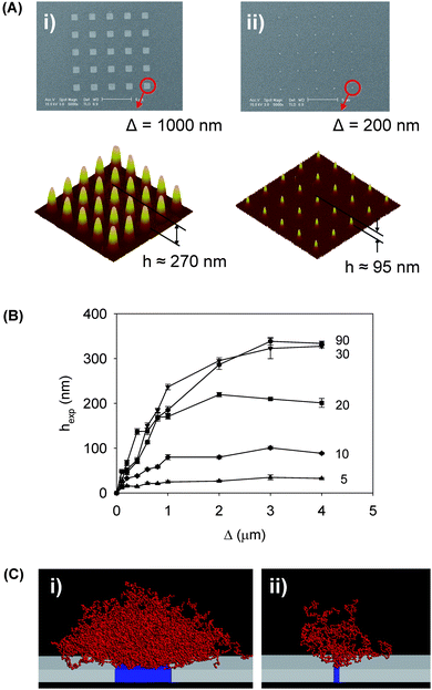 | ||
| Fig. 12 (A) SEM images of initial gold nanopatterns and tapping mode AFM images of resulting pNIPAAM polymer nanostructures after 30 minutes polymerization time imaged in air. The width of the patterned gold array was (i) Δ = 1 μm and (ii) Δ = 200 nm, resulting in brush heights (i) hexp ≈ 230 nm and (ii) hexp ≈ 55 nm after subtracting the initial gold height of 40 nm. (B) Polymer brush height as a function of footprint size and polymerization time. (C) Snapshots from molecular dynamics simulations of nanopatterned polymer brushes. Adapted with permission from ref. 128. Copyright 2007 Wiley-VCH. | ||
Various tools, including ellipsometry, X-ray deflection, and neutron reflection (NR), have been used to resolve details of the vertical structure of polymer brushes on surfaces. Among these methods, NR has perhaps the largest resolution in the Z-direction. In recent work by Zhang et al.,130 segment density profiles, obtained from NR measurements on temperature-responsive pNIPAAM polymer brushes (∼200 nm height), were fitted with predicted density profiles obtained from lattice mean-field theory. This approach provided an excellent fit to the data and involved significantly fewer independent fitting parameters than traditional NR fitting methods, involving layers of uniform densities. This is another example of the synergistic use of computer simulations and experiments, applied here to study the conformational behavior of polymer brushes.
6 Conclusions and future trends
The fabrication of patterned polymeric and biomacromolecular brush nanostructures with controlled shape, feature dimension, spacing and chemical functionality (selected examples are summarized in Table 1) represents an exciting challenge in nanotechnology. The ability to fabricate such materials is needed, for example, in the development of devices for high-throughput experimentation at the genomic and proteomic levels, in biosensing, molecular therapeutics, and drug delivery. This need is reflected in the rapidly growing number of publications in this field.| Fabrication techniques | Polymers and polymerization methods | Feature size | Author(s) and references |
|---|---|---|---|
| FRP: free radical polymerization, NMFRP: nitroxide-mediated “living” free radical polymerization, PAN: poly(aniline), PCOT: poly-cyclooctatetraene, PDMAEMA: poly(2-(dimethylamino)ethyl methacrylate), PENB: poly-5-ethylidene-2-norbornene, PHEMA: poly(2-hydroxyethyl methacrylate), PMMA: poly(methyl methacrylate), PNB: poly(norbornene), PNIPAAM: poly(N-isopropylacrylamide), PS: poly(styrene), PS-b-P2 VP-b-PEO: poly(styrene-block-2-vinyl pyridine-block-ethylene oxide), PtBA: poly(tert-butyl acrylate), RAFT: reversible addition–fragmentation chain transfer, ROMP: ring-opening metathesis polymerization, SI-ATRP: surface initiated atom transfer radical polymerization. | |||
| Photolithography and plasmonic lithography | PtBA, NM-FRP | 4 μm | Husemann et al.42 |
| PMMA, PHEMA, PDMAEMA, SI-ARTP | 100 μm | Zhou et al.26 | |
| Electron beam (chemical) lithography | PNIPAAM, SI-ATRP | 50 nm | Brough et al.33 |
| Grunze et al.50,51 | |||
| Steenackers et al.53 | |||
| Ballav et al.55 | |||
| Soft lithography | PMMA, PHEMA, PDMAEMA, SI-ATRP | Nanogap 100 nm | Zhou et al.62 |
| Capillary force lithography | PS, SI-ATRP | 100 nm | Liu et al.68 |
| Nanoshaving and nanografting | PNIPAAM, SI-ATRP | 300 nm | Kaholek et al.90 |
| Dip-pen nanolithography | PNB, ROMP | 78 nm | Liu et al.91 |
| Anodization lithography | PCOT and PENB, ROMP | 200 nm | Lee et al.99 |
| Nanoparticle templates as a lithographic tool | PNIPAAM, SI-ATRP | 30 nm | Mitsuishi et al.108 |
| Polymer brushes on nanostructures (inorganic substrates, carbon nanotubes) | PS-b-P2 VP-b-PEO, SI-ATRP | Motornov et al.110 | |
| PMMA, SI-ATRP | 200 nm | Baskaran et al.117 | |
| PNIPAAM, SI-ATRP | >5 nm | Kong et al.118 | |
| PHEMA, RAFT | Pei et al.121 | ||
| Polymer brushes on nanostructures (organic and biomolecular substrates) | PAN, FRP | 3 nm | Ma et al.124 |
Recent research has successfully begun to combine various nanolithographic and templating techniques with surface initiated polymerizations, to fabricate nanopatterned, densely packed brush structures. Yet many demonstrations of patterned brush nanostructures are still at the level of proof-of-concept. To advance the field, the potential of a broader range of polymers and biomacromolecules needs to be tapped, and, in order to tune brush surface chemistry, improved strategies for their controlled, terminal chemical functionalization need to be developed. Access to a broader spectrum of stimulus-responsive polymers will be important for the hierarchical fabrication of functional brush nanostructures. Finally, new strategies for SIP of biomolecules need to be devised. Specifically, the potential of directed self-assembly of oligomeric biomolecular building blocks into grafted brushes needs to be explored further, because such a biomolecular ‘Lego’ scheme could provide the key towards the fabrication of densely packed biomacromolacular nanostructures on surfaces.
The ability to fabricate nanopatterned polymer brushes relies largely on the quality of the substrate patterns. While to date most patterning strategies have been adapted from established lithographic approaches, the potential of using lithographic methods to chemically modify and functionalize substrate surfaces has largely not been tapped. An exciting new development in this area is electron-beam chemical lithography, which has evolved as one promising new strategy to exert direct control over surface chemistries and to fabricate topographic gradients in polymeric brush nanostructures. In addition, the emerging field of plasmonic lithography will be of particular interest to pattern and chemically modify surfaces, and promises great potential for the fabrication of polymeric nanostructures.
Recent research activities have been directed increasingly more towards broadening the available chemical functionalities, while further improving the control over architecture and structural complexity. These developments will also drive critical research directed to better understanding and manipulating the structure–property relationships of polymeric and biomolecular brush nanostructures, and ultimately help to transition these materials into useful applications.
Acknowledgements
SZ gratefully acknowledges the National Science Foundation for support through an NSF DMR-0239769 CAREER AWARD and through grant NSF DMR-0502953.References
- N. Dan, Trends Biotechnol., 2000, 18, 370–374 CrossRef CAS.
- B. Zhao and W. J. Brittain, Prog. Polym. Sci., 2000, 25, 677–710 CrossRef CAS.
- S. T. Milner, T. A. Witten and M. E. Cates, Macromolecules, 1988, 21, 2610–2619 CrossRef CAS.
- Polymer Brushes, ed. R. C. Advincula, W. J. Brittain, K. C. Caster and J. Rühe, WILEY-VCH Verlag GmbH & Co, Weinheim, 2004 Search PubMed.
- J. C. Love, L. A. Estroff, J. K. Kriebel, R. G. Nuzzo and G. M. Whitesides, Chem. Rev., 2005, 105, 1103–1169 CrossRef CAS.
- A. S. Blawas and W. M. Reichert, Biomaterials, 1998, 19, 595–609 CrossRef CAS.
- M. Mrksich and G. M. Whitesides, Trends Biotechnol., 1995, 13, 228–235 CrossRef CAS.
- D. J. Beebe, J. S. Moore, Q. Yu, R. H. Liu, M. L. Kraft, B. H. Jo and C. Devadoss, Proc. Natl. Acad. Sci. U. S. A., 2000, 97, 13488–13493 CrossRef CAS.
- S. Edmondson, V. L. Osborne and W. T. S. Huck, Chem. Soc. Rev., 2004, 33, 14–22 RSC.
- O. Prucker and J. Rühe, Macromolecules, 1998, 31, 602–613 CrossRef CAS.
- J. Hyun, W. K. Lee, N. Nath, A. Chilkoti and S. Zauscher, J. Am. Chem. Soc., 2004, 126, 7330–7335 CrossRef CAS.
- G. Tovar, S. Paul, W. Knoll, O. Prucker and J. Rühe, Supramol. Sci., 1995, 2, 89–98 CrossRef CAS.
- R. Jordan and A. Ulman, J. Am. Chem. Soc., 1998, 120, 243–247 CrossRef CAS.
- A. Ulman, Chem. Rev., 1996, 96, 1533–1554 CrossRef CAS.
- W. Senaratne, L. Andruzzi and C. K. Ober, Biomacromolecules, 2005, 6, 2427–2448 CrossRef CAS.
- O. Prucker and J. Rühe, Macromolecules, 1998, 31, 592–601 CrossRef.
- R. Jordan, A. Ulman, J. F. Kang, M. H. Rafailovich and J. Sokolov, J. Am. Chem. Soc., 1999, 121, 1016–1022 CrossRef CAS.
- M. D. K. Ingall, C. H. Honeyman, J. V. Mercure, P. A. Bianconi and R. R. Kunz, J. Am. Chem. Soc., 1999, 121, 3607–3613 CrossRef CAS.
- W. Chen, A. Y. Fadeev, M. C. Hsieh, D. Oner, J. Youngblood and T. J. McCarthy, Langmuir, 1999, 15, 3395–3399 CrossRef CAS.
- M. Husemann, D. Mecerreyes, C. J. Hawker, J. L. Hedrick, R. Shah and N. L. Abbott, Angew. Chem., Int. Ed., 1999, 38, 647–649 CrossRef.
- O. Prucker, C. A. Naumann, J. Rühe, W. Knoll and C. W. Frank, J. Am. Chem. Soc., 1999, 121, 8766–8770 CrossRef CAS.
- C. Gurtner, A. W. Wun and M. Sailor, Angew. Chem., Int. Ed., 1999, 38, 1966–1968 CrossRef CAS.
- R. H. Grubbs and S. Chang, Tetrahedron, 1998, 54, 4413–4450 CrossRef CAS.
- K. Matyjaszewski and J. H. Xia, Chem. Rev., 2001, 101, 2921–2990 CrossRef CAS.
- T. E. Patten and K. Matyjaszewski, Acc. Chem. Res., 1999, 32, 895–903 CrossRef CAS.
- F. Zhou, L. Jiang, W. M. Liu and Q. J. Xue, Macromol. Rapid Commun., 2004, 25, 1979–1983 CrossRef CAS.
- G. Carrot, S. Diamanti, M. Manuszak, B. Charleux and I. P. Vairon, J. Polym. Sci., Part A: Polym. Chem., 2001, 39, 4294–4301 CrossRef CAS.
- D. Xiao, H. Zhang and M. Wirth, Langmuir, 2002, 18, 9971–9976 CrossRef CAS.
- J. Pietrasik, H. Dong and K. Matyjaszewski, Macromolecules, 2006, 39, 6384–6390 CrossRef CAS.
- J. Pyun, T. Kowalewski and K. Matyjaszewski, Macromol. Rapid Commun., 2003, 24, 1043–1059 CrossRef CAS.
- D. C. Chow, W. K. Lee, S. Zauscher and A. Chilkoti, J. Am. Chem. Soc., 2005, 127, 14122–14123 CrossRef CAS.
- G. Y. Liu and N. A. Amro, Proc. Natl. Acad. Sci. U. S. A., 2002, 99, 5165–5170 CrossRef CAS.
- B. Brough, K. L. Christman, T. S. Wong, C. M. Kolodziej, J. G. Forbes, K. Wang, H. D. Maynard and C. M. Ho, Soft Matter, 2007, 3, 541–546 RSC.
- M. Mrksich, Chem. Soc. Rev., 2000, 29, 267–273 RSC.
- D. C. Chow and A. Chilkoti, Langmuir, 2007, 23, 11712–11717 CrossRef CAS.
- E. Menard, M. A. Meitl, Y. G. Sun, J. U. Park, D. J. L. Shir, Y. S. Nam, S. Jeon and J. A. Rogers, Chem. Rev., 2007, 107, 1117–1160 CrossRef CAS.
- M. Lundstrom, Science, 2003, 299, 210–211 CrossRef CAS.
- T. Ito and S. Okazaki, Nature, 2000, 406, 1027–1031 CrossRef CAS.
- M. Totzeck, W. Ulrich, A. Gohnermeier and W. Kaiser, Nat. Photonics, 2007, 1, 629–631 Search PubMed.
- R. C. Dunn, Chem. Rev., 1999, 99, 2891–2927 CrossRef CAS.
- O. Prucker, M. Schimmel, G. Tovar, W. Knoll and J. Rühe, Adv. Mater., 1998, 10, 1073–1077 CrossRef CAS.
- M. Husemann, M. Morrison, D. Benoit, K. J. Frommer, C. M. Mate, W. D. Hinsberg, J. L. Hedrick and C. J. Hawker, J. Am. Chem. Soc., 2000, 122, 1844–1845 CrossRef CAS.
- O. Prucker, J. Habicht, I. J. Park and J. Rühe, Mater. Sci. Eng., C, 1999, 8–9, 291–297 CrossRef.
- C. Padeste, H. H. Solak, H. P. Brack, M. Slaski, S. A. Gursel and G. G. Scherer, J. Vac. Sci. Technol., B, 2004, 22, 3191–3195 CrossRef CAS.
- W. Srituravanich, N. Fang, C. Sun, Q. Luo and X. Zhang, Nano Lett., 2004, 4, 1085–1088 CrossRef CAS.
- N. Fang, H. Lee, C. Sun and X. Zhang, Science, 2005, 308, 534–537 CrossRef CAS.
- M. M. Alkaisi, R. J. Blaikie and S. J. McNab, Adv. Mater., 2001, 13, 877–887 CrossRef CAS.
- M. J. Lercel, H. G. Craighead, A. N. Parikh, K. Seshadri and D. L. Allara, Appl. Phys. Lett., 1996, 68, 1504–1506 CrossRef CAS.
- S. J. Ahn, M. Kaholek, W. K. Lee, B. LaMattina, T. H. LaBean and S. Zauscher, Adv. Mater., 2004, 16, 2141–2145 CrossRef CAS.
- W. Eck, V. Stadler, W. Geyer, M. Zharnikov, A. Golzhauser and M. Grunze, Adv. Mater., 2000, 12, 805–808 CrossRef CAS.
- A. Golzhauser, W. Eck, W. Geyer, V. Stadler, T. Weimann, P. Hinze and M. Grunze, Adv. Mater., 2001, 13, 803–806 CrossRef.
- U. Schmelmer, A. Paul, A. Kuller, M. Steenackers, A. Ulman, M. Grunze, A. Golzhauser and R. Jordan, Small, 2007, 3, 459–465 CrossRef CAS.
- M. Steenackers, A. Küller, N. Ballav, M. Zharnikov, M. Grunze and R. Jordan, Small, 2007, 3, 1764–1773 CrossRef CAS.
- Q. He, A. Kueller, S. Schilp, F. Leisten, H.-A. Kolb, M. Grunze and J. Li, Small, 2007, 3, 1860–1865 CrossRef CAS.
- Nirmalya Ballav, Soeren Schilp and M. Zharnikov, Angew. Chem., Int. Ed., 2008, 47, 1421–1424 CrossRef CAS.
- Y. N. Xia and G. M. Whitesides, Angew. Chem., Int. Ed., 1998, 37, 551–575 CrossRef CAS.
- A. Kumar and G. M. Whitesides, Appl. Phys. Lett., 1993, 63, 2002–2004 CrossRef.
- N. L. Jeon, I. S. Choi, G. M. Whitesides, N. Y. Kim, P. E. Laibinis, Y. Harada, K. R. Finnie, G. S. Girolami and R. G. Nuzzo, Appl. Phys. Lett., 1999, 75, 4201–4203 CrossRef CAS.
- Y. Jun, D. Le and X. Y. Zhu, Langmuir, 2002, 18, 3415–3417 CrossRef CAS.
- H. Tu, C. E. Heitzman and P. V. Braun, Langmuir, 2004, 20, 8313–8320 CrossRef CAS.
- H. W. Ma, J. H. Hyun, P. Stiller and A. Chilkoti, Adv. Mater., 2004, 16, 338–341 CrossRef CAS.
- F. Zhou, Z. J. Zheng, B. Yu, W. M. Liu and W. T. S. Huck, J. Am. Chem. Soc., 2006, 128, 16253–16258 CrossRef CAS.
- D. J. Dyer, Adv. Funct. Mater., 2003, 13, 667–670 CrossRef CAS.
- O. Azzaroni, A. A. Brown and W. T. S. Huck, Angew. Chem., Int. Ed., 2006, 45, 1770–1774 CrossRef CAS.
- S. Moya, O. Azzaroni, T. Farhan, V. L. Osborne and W. T. S. Huck, Angew. Chem., Int. Ed., 2005, 44, 4578–4581 CrossRef CAS.
- T. W. Odom, V. R. Thalladi, J. C. Love and G. M. Whitesides, J. Am. Chem. Soc., 2002, 124, 12112–12113 CrossRef CAS.
- H. W. Li, B. V. O. Muir, G. Fichet and W. T. S. Huck, Langmuir, 2003, 19, 1963–1965 CrossRef CAS.
- Y. Liu, V. Klep and I. Luzinov, J. Am. Chem. Soc., 2006, 128, 8106–8107 CrossRef CAS.
- K. Y. Suh, S. J. Choi, S. J. Baek, T. W. Kim and R. Langer, Adv. Mater., 2005, 17, 560–564 CrossRef CAS.
- G. Binnig and H. Rohrer, Helv. Phys. Acta, 1982, 55, 726–735 CAS.
- G. Binnig, C. F. Quate and C. Gerber, Phys. Rev. Lett., 1986, 56, 930–933 CrossRef.
- C. A. Mirkin and J. A. Rogers, MRS Bull., 2001, 26, 506–508 CAS.
- G. Y. Liu, S. Xu and Y. L. Qian, Acc. Chem. Res., 2000, 33, 457–466 CrossRef CAS.
- S. Xu and G. Y. Liu, Langmuir, 1997, 13, 127–129 CrossRef CAS.
- S. Xu, S. Miller, P. E. Laibinis and G. Y. Liu, Langmuir, 1999, 15, 7244–7251 CrossRef CAS.
- H. Sugimura and N. Nakagiri, J. Vac. Sci. Technol., A, 1996, 14, 1223–1227 CrossRef CAS.
- B. Legrand and D. Stievenard, Appl. Phys. Lett., 1999, 74, 4049–4051 CrossRef CAS.
- H. Sugimura, O. Takai and N. Nakagiri, J. Vac. Sci. Technol., B, 1999, 17, 1605–1608 CrossRef CAS.
- H. Sugimura, K. Okiguchi and N. Nakagiri, Jpn. J. Appl. Phys., Part 2, 1996, 35, 3749–3753 CrossRef CAS.
- F. P. Zamborini and R. M. Crooks, J. Am. Chem. Soc., 1998, 120, 9700–9701 CrossRef CAS.
- C. B. Gorman, R. L. Carroll, Y. F. He, F. Tian and R. Fuierer, Langmuir, 2000, 16, 6312–6316 CrossRef CAS.
- R. Maoz, E. Frydman, S. R. Cohen and J. Sagiv, Adv. Mater., 2000, 12, 725–731 CrossRef CAS.
- R. Maoz, E. Frydman, S. R. Cohen and J. Sagiv, Adv. Mater., 2000, 12, 424–429 CrossRef CAS.
- R. M. Nyffenegger and R. M. Penner, Chem. Rev., 1997, 97, 1195–1230 CrossRef CAS.
- A. J. Bard, G. Denuault, C. Lee, D. Mandler and D. O. Wipf, Acc. Chem. Res., 1990, 23, 357–363 CrossRef CAS.
- E. S. Snow and P. M. Campbell, Science, 1995, 270, 1639–1641 CrossRef CAS.
- R. D. Piner, J. Zhu, F. Xu, S. H. Hong and C. A. Mirkin, Science, 1999, 283, 661–663 CrossRef CAS.
- B. W. Maynor, S. F. Filocamo, M. W. Grinstaff and J. Liu, J. Am. Chem. Soc., 2002, 124, 522–523 CrossRef CAS.
- J. R. Kenseth, J. A. Harnisch, V. W. Jones and M. D. Porter, Langmuir, 2001, 17, 4105–4112 CrossRef CAS.
- M. Kaholek, W. K. Lee, B. LaMattina, K. C. Caster and S. Zauscher, Nano Lett., 2004, 4, 373–376 CrossRef CAS.
- X. G. Liu, S. W. Guo and C. A. Mirkin, Angew. Chem., Int. Ed., 2003, 42, 4785–4789 CrossRef CAS.
- K. Salaita, Y. Wang and C. A. Mirkin, Nat. Nano, 2007, 2, 145–155 Search PubMed.
- S. H. Hong, J. Zhu and C. A. Mirkin, Science, 1999, 286, 523–525 CrossRef CAS.
- S.-J. Ahn, W.-K. Lee and S. Zauscher, in Bioinspired Nanoscale Hybrid Systems, ed. G. Schmid, U. Simon, S. J. Stranick, S. M. Arrivo and S. Hong, Materials Research Society, Warrendale, PA, 2003, vol. 735, pp. C11.54.11–C11.54.16 Search PubMed.
- M. Kaholek, W.-K. Lee, B. LaMattina, K. C. Caster and S. Zauscher, in Polymer Brushes: From Synthesis to Functional Microstructures, ed. W. J. Brittain, R. C. Advincula, J. Rühe and K. C. Caster, John Wiley & Sons, New York, 2004, pp. 381–402 Search PubMed.
- S. Zapotoczny, E. M. Benetti and G. J. Vancso, J. Mater. Chem., 2007, 17, 3293–3296 RSC.
- Y. Li, B. W. Maynor and J. Liu, J. Am. Chem. Soc., 2001, 123, 2105–2106 CrossRef CAS.
- J. A. Dagata, J. Schneir, H. H. Harary, C. J. Evans, M. T. Postek and J. Bennett, Appl. Phys. Lett., 1990, 56, 2001–2003 CrossRef CAS.
- W. K. Lee, K. C. Caster, J. Kim and S. Zauscher, Small, 2006, 2, 848–853 CrossRef CAS.
- G. J. Leggett, Chem. Soc. Rev., 2006, 35, 1150–1161 RSC.
- S. Wegscheider, A. Kirsch, J. Mlynek and G. Krausch, Thin Solid Films, 1995, 264, 264–267 CrossRef CAS.
- E. Betzig and J. K. Trautman, Science, 1992, 257, 189–195 CrossRef CAS.
- R. E. Ducker and G. J. Leggett, J. Am. Chem. Soc., 2006, 128, 392–393 CrossRef CAS.
- L. Novotny and S. J. Stranick, Annu. Rev. Phys. Chem., 2006, 57, 303–331 CrossRef CAS.
- G. Wurtz, R. Bachelot, F. H'Dhili, P. Royer, C. Triger, C. Ecoffet and D. J. Lougnot, Jpn. J. Appl. Phys., Part 2, 2000, 39, L98–L100 CrossRef CAS.
- J. Shan and H. Tenhu, Chem. Commun., 2007, 4580–4598 RSC.
- M. Uchida, M. T. Klem, M. Allen, P. Suci, M. Flenniken, E. Gillitzer, Z. Varpness, L. O. Liepold, M. Young and T. Douglas, Adv. Mater., 2007, 19, 1025–1042 CrossRef CAS.
- M. Mitsuishi, Y. Koishikawa, H. Tanaka, E. Sato, T. Mikayama, J. Matsui and T. Miyashita, Langmuir, 2007, 23, 7472–7474 CrossRef CAS.
- A. C. Balazs, T. Emrick and T. P. Russell, Science, 2006, 314, 1107–1110 CrossRef CAS.
- M. Motornov, R. Sheparovych, R. Lupitskyy, E. MacWilliams, O. Hoy, I. Luzinov and S. Minko, Adv. Funct. Mater., 2007, 17, 2307–2314 CrossRef CAS.
- T. Morinaga, M. Ohkura, K. Ohno, Y. Tsujii and T. Fukuda, Macromolecules, 2007, 40, 1159–1164 CrossRef CAS.
- E. R. Zubarev, J. Xu, A. Sayyad and J. D. Gibson, J. Am. Chem. Soc., 2006, 128, 15098–15099 CrossRef CAS.
- B. P. Khanal and E. R. Zubarev, Angew. Chem., Int. Ed., 2007, 46, 2195–2198 CrossRef CAS.
- S. P. Adiga and D. W. Brenner, Nano Lett., 2005, 5, 2509–2514 CrossRef CAS.
- Y. Ito, Y. S. Park and Y. Imanishi, Langmuir, 2000, 16, 5376–5381 CrossRef CAS.
- M. Motornov, R. Sheparovych, E. Katz and S. Minko, ACS Nano, 2008, 2, 41–52 CrossRef CAS.
- D. Baskaran, J. W. Mays and M. S. Bratcher, Angew. Chem., Int. Ed., 2004, 43, 2138–2142 CrossRef CAS.
- H. Kong, W. Li, C. Gao, D. Yan, Y. Jin, D. R. M. Walton and H. W. Kroto, Macromolecules, 2004, 37, 6683–6686 CrossRef CAS.
- C. Gao, S. Muthukrishnan, W. Li, J. Yuan, Y. Xu and A. H. E. Muller, Macromolecules, 2007, 40, 1803–1815 CrossRef CAS.
- G. Guo, D. Yang, C. Wang and S. Yang, Macromolecules, 2006, 39, 9035–9040 CrossRef CAS.
- X. W. Pei, J. C. Hao and W. M. Liu, J. Phys. Chem. C, 2007, 111, 2947–2952 CrossRef CAS.
- Y. Lu, Y. Mei, R. Walker, M. Ballauff and M. Drechsler, Polymer, 2006, 47, 4985–4995 CrossRef CAS.
- M. C. Erik, W. Edwards, D. Wang and H. Möhwald, Angew. Chem., Int. Ed., 2008, 47, 320–323 CrossRef.
- Y. Ma, J. Zhang, G. Zhang and H. He, J. Am. Chem. Soc., 2004, 126, 7097–7101 CrossRef CAS.
- L. A. McDonnell and R. M. A. Heeren, Mass Spectrom. Rev., 2007, 26, 606–643 CrossRef CAS.
- S. Yunus, A. Delcorte, C. Poleunis, P. Bertrand, A. Bolognesi and C. Botta, Adv. Funct. Mater., 2007, 17, 1079–1084 CrossRef CAS.
- I. Tokareva, I. Tokarev, S. Minko, E. Hutter and J. H. Fendler, Chem. Commun., 2006, 3343–3345 RSC.
- W. K. Lee, M. Patra, P. Linse and S. Zauscher, Small, 2007, 3, 63–66 CrossRef CAS.
- M. Patra and P. Linse, Nano Lett., 2006, 6, 133–137 CrossRef CAS.
- J. Zhang, T. Nylander, R. A. Campbell, A. R. Rennie, S. Zauscher and P. Linse, Soft Matter, 2008, 4, 500–509 RSC.
| This journal is © The Royal Society of Chemistry 2008 |