Tuning the optical and photoelectrochemical properties of surface-modified TiO2†
Radim
Beranek
and
Horst
Kisch
*
Institut für Anorganische Chemie der Universität Erlangen-Nürnberg, Erlangen, Germany. E-mail: horst.kisch@chemie.uni-erlangen.de; Fax: (+49)9131-8527363; Tel: (+49)9131-8527363
First published on 12th November 2007
Abstract
Surface-modification of TiO2 is found to be a powerful tool for manipulating the fundamental optical and photoelectrochemical properties of TiO2. High surface area nanocrystalline TiO2 was modified by urea pyrolysis products at different temperatures between 300 °C and 500 °C. Modification occurs through incorporation of nitrogen species containing carbon into the surface structure of titania. The N1s XPS binding energies are 399–400 eV and decrease with increasing modification temperature whereby the Ti2p3/2 peak is also shifted to lower binding energies by about 0.5 eV. With increasing modification temperature the optical bandgap of surface-modified TiO2 continuously decreases down to ∼2.1 eV and the quasi-Fermi level of electrons at pH 7 is gradually shifted from –0.6 V to –0.3 V vs.NHE. The surface-modified materials show enhanced sub-bandgap absorption (Urbach tail) and exhibit photocurrents in the visible down to 750 nm. The maximum incident photon-to-current efficiency (IPCE) was observed for the materials modified at 350 °C and 400 °C (IPCE ∼ 14% at 400 nm, and IPCE ∼ 1% at 550 nm, respectively). The efficiency of photocurrent generation is limited by surface recombination, which leads to a significant decrease in IPCE values and significantly changes the shape of the IPCE spectra in dependence on the optical bandgap.
Introduction
Semiconductor materials have played a key role in the rapid development of electronic and information processing technologies for several decades. More recently, it has been recognized that the utilization of semiconductors represents a major challenge also for photochemistry. In this context, it is of fundamental importance that semiconductors enable efficient light-induced generation and separation of charges which can subsequently undergo redox reactions with substrates or induce a photocurrent.1 This opens up a route to various applications in photocatalysis, photovoltaics and sensor technology.2–12 Obviously, in order to achieve optimal performance, semiconductors with well-tailored optical and photoelectrochemical properties are required in most applications. The development of methods allowing control of these semiconductor properties attracts therefore significant interest.13–19One of the most promising semiconductors for photoelectrochemical applications is titanium dioxide, particularly due to its low cost, non-toxicity, and stability against photocorrosion.5,20–24 However, because of its wide bandgap (for anatase 3.2 eV; ∼390 nm) the utilization of TiO2 remains confined to UV light. Shifting the threshold of its photoresponse into the visible might therefore enhance its potential for chemical solar energy conversion and open possibilities for further applications. Attempts to achieve this have typically used sensitization with organic dyes,25,26 transition metal complexes27,28 or quantum dots.29–31 Another strategy consists in doping TiO2 with transition metals17,32,33 or main group elements like carbon,34–38nitrogen39–47 and sulfur.48,49 Amongst these, particularly the nitrogen doping has been found very promising since calculations suggested that it might narrow the TiO2 bandgap and thereby promote also visible light photoactivity.41,50 In recent years N-modified TiO2 materials have been prepared, for example, by calcining titanium hydroxide with aqueous ammonia40 or with an ammonium salt,42calcining TiO2 at 550–600 °C under an atmosphere of ammonia and argon,41 treating TiO2nanoparticles with triethylamine at room temperature,46,51 mechanochemical methods,52 DC magnetron or radio-frequency sputtering,44,53 ion implantation,54,55 or by calcining solid mixtures of titania or titanium hydroxide and urea.56,57 The debate on the nature of nitrogen incorporation in these materials remains still unsettled. X-Ray photoelectron studies typically afford N1s binding energies of ∼396 eV and/or ∼400 eV but the assignment of these peaks has been a source of controversy.58,59 Thus, the first value suggests the presence of nitridic (substitutional) nitrogen,41,53,56 the latter points to molecularly chemisorbed γ-N2,41 interstitial NH species,60hyponitrite42,43 or to an NO site within the TiO2 lattice.59,61–63 Recently, it has been also suggested that the visible light absorption of N-doped TiO2 might be solely due to the formation of oxygen vacancies and color centers associated with them.64
Drawing on our work on N-modified TiO2 powders for visible light photocatalysis42,43,57 we have recently investigated also N-modified TiO2electrodes as potential systems for visible light photovoltaics.65 These electrodes were compact ∼75 nm thick anodic TiO2 films surface-modified by heating at 400 °C in the presence of urea pyrolysis products. Using this modification method we were able to observe photocurrents in the visible down to 700 nm, which differs significantly from the photocurrent onset wavelength of ∼550 nm typically reported for N-doped TiO2.66–69 It was concluded that the photocurrent response in the visible was due to the presence of nitrogen-centered surface states positioned energetically above the valence band edge, which is in line with previously reported experimental42,44,50,68,70–72 and theoretical41,63,71,73 results for N-doped TiO2. Since the modification of the films occurred predominantly in the thin surface layer the visible light absorption was rather poor, which resulted in low values of incident photon-to-current efficiency (IPCE ∼ 1.5% at 400 nm).
As a next step we have therefore modified nanocrystalline high surface area TiO2 material by an analogous urea pyrolysis method. This could enable higher photocurrent generation efficiency due to the multiple reflection and better absorption of light in the porous structure of the electrodes.26 Furthermore, high surface/volume ratio of the starting material should presumably enhance the effect of surface modification on the properties of the material. In this paper we report detailed investigations of these novel photoelectrode materials. It is found that by simply varying the modification temperature the fundamental optical and photoelectrochemical properties of surface-modified TiO2 can be systematically controlled.
Experimental
Commercially available TiO2 powder (Hombikat UV 100, Sachtleben, Germany, anatase, specific surface area (BET) ∼300 m2 g–1, crystallite size <10 nm) was used as a starting material. For modification65 0.5 g of the powder was placed into a 230 ml Schlenk tube connected via an adapter with a 100 ml round bottom flask containing 1 g of urea and heated in a muffle oven for 30 min at different temperatures.The elemental analysis of the samples was characterized by Carlo Erba, CHNSO, E.A.1108 equipped with a pyrolysis unit (HT Sauerstoffanalysator, Hekatech) for oxygen analysis. X-Ray photoelectron spectroscopy was performed using a PHI 5600 XPS instrument. Samples for XPS measurements were pressed pellets of the powder attached to aluminum foil by silver lacquer. Argon ion sputtering was performed using a Penning source, Specs PS IQP 10/63 (p = 10–8 Torr; voltage = 3.5 kV) and the sputtering rate was estimated by calibration using a SiO2 standard of known thickness. All XPS spectra were referenced to the C1s peak at 284.8 eV from the adventitious hydrocarbon contamination. Fitting of the XPS data was accomplished using XPSPEAK41 software. A Shirley-type background subtraction was used. Diffuse reflectance spectra were obtained relative to the reflectance of a standard (BaSO4) using a Shimadzu UV-2401 UV/Vis recording spectrophotometer equipped with a diffuse reflectance accessory. The samples were pressed pellets of a mixture of 2 g of BaSO4 with 50 mg of the powder. X-Ray diffraction measurements were performed with a Philips X′Pert PW 3040/60 diffractometer. Surface area was determined by the BET (Brunauer–Emmett–Teller) method using a Gemini 2370 V.01 instrument. Density of surface OH-groups was determined by TGA analysis (Universal V2.6D TA Instrument; nitrogen atmosphere; temperature range: 24–1000 °C; heating rate = 10 °C min–1 with a 60 min isothermal step at 200 °C) assuming that the weight loss between 200 °C and 1000 °C is due to dehydroxylation of the surface.
The values of quasi-Fermi level for electrons (nEF*) were determined by the method of Roy (see Electronic Supplementary Information, ESI,† for details).28,74
For photocurrent measurements electrodes consisting of a porous nanocrystalline film deposited on ITO-glass were prepared. The conducting ITO-glass substrate (Präzision Glas & Optik, Iserlohn, Germany, sheet resistance of ∼10 Ω sq.–1) was first cut into 2.5 × 1.5 cm pieces and then subsequently degreased by sonicating in acetone and boiling NaOH (0.1M), rinsed with demineralized water, and blown dry in a nitrogen stream. A suspension of 200 mg of Hombikat UV 100 TiO2 in 1 ml of ethanol was sonicated for 20 min and then deposited onto the ITO glass by doctor blading using a scotch tape as frame and spacer. The electrodes were then dried at 100 °C, covered with aluminum foil and a glass plate, pressed for 3 min at a pressure of 200 kg cm–2 using an IR pressing tool (Paul Weber, Stuttgart, Germany) according to a procedure similar to that described in literature,75 and heated in air at 450 °C for 30 min in order to ensure good electrical contact. Such a procedure yields a ∼2.5 µm thick opaque layer of TiO2 having an excellent mechanical stability. Subsequently, the electrodes were modified at different temperatures by the procedure described above. The morphology of electrodes was characterized using a high-resolution field-emission scanning electron microscope (FE-SEM, Hitachi S4800).
Photocurrent experiments were performed with a tunable monochromatic light source provided with a 1000 W Xenon lamp and a universal grating monochromator Multimode 4 (AMKO, Tornesch, Germany) with a bandwidth of 10 nm. The electrochemical setup consisted of a BAS Epsilon Electrochemistry potentiostat (BAS, West Lafayette, USA) and a three-electrode cell using a platinum counter electrode and a Ag/AgCl (3 M KCl) reference electrode. During photoelectrochemical measurements the electrodes were pressed against an O-ring of an electrochemical cell leaving a working area of 0.636 cm2. When not denoted otherwise, the photocurrent experiments were carried out in a LiClO4 (0.1 M) containing KI (0.1 M) as a hole scavenger. Nitrogen was passed through the electrolyte prior to the experiment whereas it was supplied only to the gas phase above the electrolyte during the experiment. The wavelength dependence of photocurrent was measured at a constant potential of 0.5 V vs.Ag/AgCl. The electrodes were irradiated from the backside (through the ITO glass) with light and dark phases of 5 and 10 s, respectively. The value of photocurrent density was taken as a difference between current density under irradiation and in the dark. The incident photon-to-current efficiency (IPCE—the number of electrons generated in the external circuit divided by the number of incident photons) for each wavelength was calculated according to equation IPCE (%) = (iphhc)/(λPq) × 100, where iph is the photocurrent density, h is Planck's constant, c velocity of light, P the light power density, λ is the irradiation wavelength, and q is the elementary charge. The spectral dependence of lamp power density was measured by the optical power meter Oriel 70260 (Oriel, Stratford, USA).
Results and discussion
Fig. 1 shows the colors of powders modified at different temperatures with corresponding plots of Kubelka–Munk function F(R∞)vs. wavelength obtained from diffuse reflectance data.76 With increasing the modification temperature the color changes from slightly yellowish to intense yellow and orange. Correspondingly, the absorption edge shifts significantly to the visible range.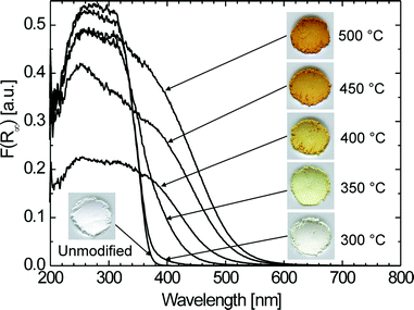 | ||
| Fig. 1 Colors and corresponding plots of Kubelka–Munk function vs. wavelength of powders modified at different temperatures. | ||
Bandgap energies Eg can be determined using the equation77α = A(hν – Eg)n/hν, where α is absorption coefficient, A is a constant, hν is the energy of light and n is a constant depending on the nature of the electron transition. Assuming an indirect bandgap (n = 2) for TiO278 and that the absorption coefficient α is proportional to Kubelka–Munk function F(R∞), the bandgap energy can be obtained from the plots of [F(R∞)hν]1/2vs.hν as the intercept at [F(R∞)hν]1/2 = 0 of the extrapolated linear part of the plot (Fig. 2). Whereas unmodified TiO2 exhibits a bandgap of 3.23 ± 0.03 eV—a typical value for anatase—the bandgap of modified samples (TiO2–N) is continuously shifted down to 2.11 ± 0.03 eV with increasing modification temperature. It should be noted that such a strong red shift of the bandgap has been only rarely observed for N-modified TiO2—e.g. for materials obtained by direct amination of TiO2nanoparticles with triethylamine46,51 or, in our group, by calcining solid mixtures of titanium hydroxide and urea.57 In contrast, most of conventionally prepared N-doped TiO2 materials reported in the literature exhibit not such a complete shift of the absorption edge but rather only a small preabsorption shoulder in the visible followed by a steep increase of absorption due to the band-to-band transition in the UV region. Furthermore, the plots in Fig. 2 clearly indicate that also the typical sub-bandgap absorption tail (Urbach tail)79 is enlarged significantly after modification. The electronic states responsible for the Urbach tail are reported to be located at the surface of TiO2 particles.80,81
![Bandgap determination using [F(R∞)hν]1/2vs.hν plots (assuming indirect optical transition) for unmodified TiO2 (a) and TiO2–N modified at 300 °C (b), 350 °C (c), 400 °C (d), 450 °C (e), and 500 °C (f).](/image/article/2008/PP/b711658f/b711658f-f2.gif) | ||
| Fig. 2 Bandgap determination using [F(R∞)hν]1/2vs.hν plots (assuming indirect optical transition) for unmodified TiO2 (a) and TiO2–N modified at 300 °C (b), 350 °C (c), 400 °C (d), 450 °C (e), and 500 °C (f). | ||
During modification, according to the experimental set-up, TiO2 and urea were located in different reaction flasks connected by an adapter. Modification of the titania surface therefore has to occur by pyrolysis products of urea (ammonia, biuret, isocyanic acid, cyanamide, etc.).82 It seems unlikely that out of these ammonia is responsible for modification since it was reported that this requires a temperature of 600 °C.41X-Ray diffraction patterns (see ESI, Fig. S1†) of all samples revealed only anatase peaks. The elemental analysis (Table 1) shows that all the modified samples contain both nitrogen and carbon (weight ratio N/C = 2.2 ± 0.3). This indicates that carbon containing nitrogen species (with atomic ratio N/C of ∼2) are present, which is also supported by infrared spectra of these samples exhibiting peaks related to multiply bound CN fragments (see ESI, Fig. S2†).
| Modification temperature/°C | N (wt%) | C (wt%) | H (wt%) | O (±3 wt%) | Surface area/m2 g–1 | Crystallite size/nm |
|---|---|---|---|---|---|---|
| a Elemental analysis. b BET method. c Calculated from Scherrer formula. | ||||||
| Unmodified | — | 0.1 | 1.6 | 41 | 282 | 8 |
| 300 | 3.3 | 1.2 | 0.7 | 37 | 217 | 9 |
| 350 | 7.5 | 3.5 | 0.8 | 39 | 149 | 9 |
| 400 | 15.5 | 7.9 | 0.7 | 30 | 53 | 8 |
| 450 | 18.9 | 8.2 | 0.6 | 32 | 39 | 8 |
| 500 | 11.8 | 5.8 | 0.5 | 31 | 96 | 9 |
Evidently, the nitrogen modified surface layer possesses a much smaller amount of N2-adsorption sites, which makes itself manifest in drastically decreased BET surface area, whereas the crystallite size does not change significantly (see Table 1). The content of nitrogen is very high—the elemental analysis data yield the N/Ti atomic ratio of 0.2, 0.5, 1.2, 1.6 and 0.8 (all ±0.2) for TiO2–N modified at 300 °C, 350 °C, 400 °C, 450 °C, and 500 °C, respectively.83 These values are surprisingly higher than previously reported data for bulk modified materials.41,43,45,46,84 It seems therefore likely that species containing more than one nitrogen atom are prevalent. We also cannot exclude that not all but only a part of the species might be directly involved in modification, contributing thus to the shift of the optical absorption edge. It should be also mentioned that TiO2–N modified at 500 °C exhibits the smallest bandgap but has a lower content of nitrogen and correspondingly a higher surface area than TiO2–N modified at 400 °C. This might be explained by the enhanced rate of desorption of surface species above 450 °C as evidenced by thermogravimetric analysis (see ESI, Fig. S3†). Further evidence for the assumption that the modification is confined to the titania surface is the fact that it can be totally removed by simply treating the modified powder in boiling NaOH (5 M) for 1 h (see ESI, Fig. S4†).
The above presented data suggest that not only the absolute amount of nitrogen species but also their chemical nature and incorporation into the surface play a decisive role in the modification. We have therefore performed a detailed XPS investigation of all materials. Fig. 3(A) shows the overall and high resolution N1s and Ti2p XPS spectra (recorded without sputtering with Ar+ ions). Interestingly, the N1s peak at ∼396 eV that is thought to evidence the presence of substitutional nitrogen41,53,85 was not detected. Instead, for TiO2–N modified at 300 °C a rather broad (full width at half maximum (FWHM) = 2.2 eV) N1s signal peak at ∼400.1 eV is observed which can be ascribed to nitrogen species in a higher oxidation state—for example nitrogen species containing NC or NCO bonds,86–88 interstitial NH species60 or to an NO site within a TiO2 lattice.59,61–63,89 For materials modified at higher temperatures the peaks becomes slightly broader (FWHM = 2.7 ± 0.2 eV) and shift to lower binding energies by ca. 1 eV. The deconvolution of these peaks into narrower sub-peaks was possible but did not result in any significant trend. The shift to lower binding energies might be due to enhanced formation of N–Ti bonds, or the higher content of adsorbed ammonia90 or nitrogen species containing C–N![[double bond, length as m-dash]](https://www.rsc.org/images/entities/char_e001.gif) C bonds86,87 originating from pyrolysis products of urea. A similar trend can be observed in case of Ti2p peaks. Whereas the unmodified sample shows the Ti2p3/2 peak at 459.0 eV—a typical value for TiO291–93—a slight shift by ∼0.2 eV and 0.3 eV is observed in samples modified at 300 °C and 350 °C, respectively. For samples modified at higher temperatures the shift is even larger (0.5–0.7 eV). The shift to lower binding energies suggests that some Ti4+ atoms are partially reduced to a lower oxidation state, presumably due to the nitrogen species bound to Ti and/or to the higher amount of oxygen vacancies.93,94Fig. 3(B) displays the changes of N1s peak upon sputtering with Ar+ ions. It clearly shows that the sputtering procedure makes a new peak to appear at 396.6 eV suggesting the presence of nitridic type of nitrogen as in TiN.93 Moreover, the peak becomes larger with increasing sputtering depth, i.e. with prolonged sputtering time. This could be interpreted in terms of nitridic species present only in the deeper layers of the material. However, the fact that this peak was completely missing before sputtering seems rather to confirm the suggestion of Diwald et al. that the bombardment with Ar+ ions can induce changes of the chemical nature of nitrogen species at the surface of N-doped TiO2 and shift the N1s binding energies to 396.7 eV.60 This is, furthermore, corroborated by the fact that the sputtering also leads to intense reduction of surface Ti4+ atoms to Ti3+ through generation of oxygen vacancies—this even in the case of unmodified TiO2 (see ESI, Fig. S5†). These results indicate that attention must be paid when comparing different XPS results on N-modified TiO2 from the literature and that sputtering with Ar+ ions should be presumably avoided if the nature of nitrogen species on TiO2 surface is investigated.
C bonds86,87 originating from pyrolysis products of urea. A similar trend can be observed in case of Ti2p peaks. Whereas the unmodified sample shows the Ti2p3/2 peak at 459.0 eV—a typical value for TiO291–93—a slight shift by ∼0.2 eV and 0.3 eV is observed in samples modified at 300 °C and 350 °C, respectively. For samples modified at higher temperatures the shift is even larger (0.5–0.7 eV). The shift to lower binding energies suggests that some Ti4+ atoms are partially reduced to a lower oxidation state, presumably due to the nitrogen species bound to Ti and/or to the higher amount of oxygen vacancies.93,94Fig. 3(B) displays the changes of N1s peak upon sputtering with Ar+ ions. It clearly shows that the sputtering procedure makes a new peak to appear at 396.6 eV suggesting the presence of nitridic type of nitrogen as in TiN.93 Moreover, the peak becomes larger with increasing sputtering depth, i.e. with prolonged sputtering time. This could be interpreted in terms of nitridic species present only in the deeper layers of the material. However, the fact that this peak was completely missing before sputtering seems rather to confirm the suggestion of Diwald et al. that the bombardment with Ar+ ions can induce changes of the chemical nature of nitrogen species at the surface of N-doped TiO2 and shift the N1s binding energies to 396.7 eV.60 This is, furthermore, corroborated by the fact that the sputtering also leads to intense reduction of surface Ti4+ atoms to Ti3+ through generation of oxygen vacancies—this even in the case of unmodified TiO2 (see ESI, Fig. S5†). These results indicate that attention must be paid when comparing different XPS results on N-modified TiO2 from the literature and that sputtering with Ar+ ions should be presumably avoided if the nature of nitrogen species on TiO2 surface is investigated.
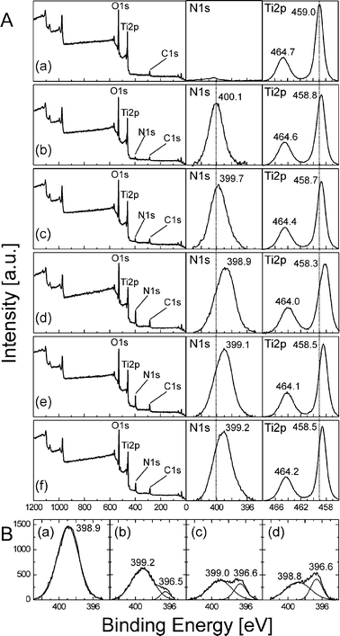 | ||
| Fig. 3 (A) Overall and high-resolution N1s and Ti2p XPS spectra (measured without sputtering with Ar+ sions) of unmodified TiO2 (a) and TiO2–N modified at 300 °C (b), 350 °C (c), 400 °C (d), 450 °C (e), and 500 °C (f). (B) High resolution N1s peak of TiO2–N modified at 400 °C recorded before (a) and after sputtering with Ar+ ions to remove the top layer with a thickness of about 1 nm (b), 5 nm (c), and 10 nm (d). | ||
Since the modification process occurs predominantly on the surface of TiO2 it can be expected that the surface properties of the starting material could influence the modification significantly. Indeed, this is the case. When the starting TiO2 material was heat pretreated at 800 °C in air for 3 h a material was obtained which had about 4 times larger crystallite size (anatase structure was retained; see ESI, Fig. S6†), about 20 times lower surface area and about 5.5 times lower concentration of surface OH-groups. Modification of this material at 400 °C afforded a modified material containing about 2.7 times lower amount of nitrogen and carbon and exhibiting a larger bandgap of 2.77 ± 0.03 eV in contrast to 2.29 ± 0.03 eV of the material modified without a heat pretreatment (see ESI, Fig. S7†).
On the basis of the above results we assume the modification process to be initiated by a reaction of the TiO2 surface with nitrogen species from urea pyrolysis containing also carbon (possibly isocyanic acid, cyanamide, or other).82 It is likely that replacement of OH-groups (and possibly also of the bridging lattice oxide ion) on the surface of TiO2 by nitrogen species plays an important role in the process. The surface of titania nanocrystals is thus chemically modified whereby the composition of the surface layer can be assumed to be TiONxCy with x/y = 2. The strong shift of the absorption edge can be rationalized by assuming that the surface-modification process gives rise to a broad nitrogen-centered energy band which overlaps with the titania valence band whereby a strong electronic coupling of N2p states with titania O2p levels may be present.50,57,84,95 It should be noted that an alternative explanation would assume that the strong shift of the absorption edge is due to a very high density of so-called color centers, as recently suggested.64
Photoelectrochemical applications require a detailed knowledge of the positions of semiconductor's band edges since these give information on the reductive and oxidative power of photogenerated electrons and holes, respectively. For heavily doped n-type metal oxides like TiO2, the lower conduction band edge, Ec, practically merges with the quasi-Fermi level for electrons, nEF*, (|Ec – nEF*| < 0.1 V).96 We determined nEF* by the method of Roy28,74 (see ESI for details, esp. Fig. S8†).
Fig. 4 shows the values of nEF* at pH = 7 in dependence on the modification temperature. Whereas nEF* of unmodified TiO2 is –0.60 ± 0.02 V vs.NHE, which is in agreement with reported values for anatase (–0.58 V vs.NHE),97nEF* of TiO2–N is continuously shifted anodically with increasing modification temperature from –0.58 ± 0.02 V at 300 °C and –0.48 ± 0.02 V at 350 °C down to –0.30 ± 0.02 V at 400 °C, 450 °C and 500 °C. The anodic shift is in line with previous reports on N-doped TiO2.42,43,53,57,65 In general, an anodic shift of nEF* (or, in other words, of the conduction band edge Ec) means that, at a given pH, the surface of TiO2–N is charged more positively than that of unmodified TiO2. Assuming incorporation of nitrogen species into the surface structure of titania in TiO2–N, the charge on the surface titanium atoms becomes less positive due to the lower electronegativity of nitrogen as compared to oxygen. This, in turn, makes more favorable the protonation of titanium bound surface species and, at the same time, the deprotonation of these species by OH– ions from the electrolyte becomes less favorable. This finally results, at a given pH, in a more positive charge at the surface as compared to the situation on unmodified TiO2. This explanation is corroborated by the fact that the amount of the anodic shift of nEF* coincides well with the shift of Ti2p3/2 peak to lower binding energies in Fig. 3(A) which indicates partial reduction of surface Ti4+ ions to lower oxidation states.
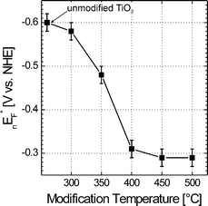 | ||
| Fig. 4 Quasi-Fermi level for electrons (nEF*) at pH = 7 determined by suspension method as a function of modification temperature. | ||
Knowing the positions of the conduction band edges, the positions of valence band edges can be obtained by simply adding the value of bandgap energy from Fig. 2. Thus, a simplified potential level diagram (Fig. 5) can be constructed which depicts the situation during the photocurrent measurements when all materials are deposited as pressed layers on ITO-glass electrodes.
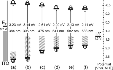 | ||
| Fig. 5 A simplified potential level diagram for photocurrent measurements with unmodified TiO2 (a) and TiO2–N modified at 300 °C (b), 350 °C (c), 400 °C (d), 450 °C (e), and 500 °C (f) deposited on ITO-glass electrodes biased at 0.5 V vs.Ag/AgCl in the presence of iodide. The positions of conduction band edges were taken as quasi-Fermi levels for electrons at pH = 7 (Fig. 4) and the positions of valence band edges were obtained by adding the value of bandgap energy from Fig. 2. Hatched areas represent surface states causing the sub-bandgap Urbach tail absorption as obtained from Fig. 2. | ||
The cross-sectional views of the electrodes (Fig. 6) show the porous morphology of the ∼2.5 µm thick nanocrystalline layer on ITO-glass which can be easily permeated by electrolyte. Here two points are noteworthy. First, in contrast to compact semiconductor electrodes, the photogenerated charge separation in such highly porous nanocrystalline electrodes is not controlled by the potential gradient over the space charge region since formation of a space charge layer is improbable due to the small crystallite size.98,99 Instead, the photocurrent is determined by the efficiency of photogenerated electron/hole transfer at the semiconductor/electrolyte and semiconductor/ITO interface.100–103 Since the electron transfer from the porous network of particles into the ITO layer can be assumed to occur readily because the Fermi level of the anodically biased ITO layer (EF ∼ 0.7 V vs.NHE) lies well below the conduction band edge of all materials, it is the interfacial hole reaction which exerts a crucial influence on the photocurrent response of the electrode. In other words, in order to observe photocurrents the photogenerated hole must react with a reducing agent present in the electrolyte. If no suitable hole scavenger is present, the photogenerated holes are doomed to recombine with the conduction band electrons and do not contribute to the photocurrent. In our previous investigations we found that the holes photogenerated in N-modified TiO2 materials are highly efficiently trapped at deep intra-bandgap surface states (the hatched area in Fig. 5) before they react with the reducing agent in the electrolyte.95 In aqueous electrolytes this leads to enhanced recombination since the reacting holes are not positive enough to induce oxidation of watervia the OH radical which requires a potential of ∼2.0 V vs.NHE at pH 7.104 This recombination can be suppressed by addition of more easily oxidizable species like iodide (E° ∼ 1.3 V vs.NHE).104 Indeed, also in the present study we observed that addition of iodide diminished the surface recombination and leads to two- to three-fold enhancement of photocurrents in the visible (see ESI, Fig. S9†).
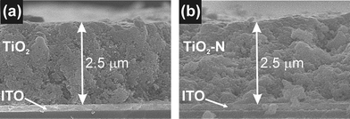 | ||
| Fig. 6 Scanning electron micrograph of a cross-section of unmodified TiO2 (a) and TiO2–N modified at 400 °C (b) deposited on ITO-glass substrate . The electrodes were mechanically fractioned. | ||
Fig. 7 shows IPCE action spectra of all electrodes in a LiClO4 electrolyte containing iodide. In contrast to unmodified TiO2 the modified TiO2–N electrodes show significant photocurrent response in the visible. In accordance with the optical absorption properties of the materials (Fig. 1 and 2) the IPCE values typically decrease exponentially down to 700–750 nm. This differs from the photocurrent onset wavelength of ∼550 nm typically reported for N-doped TiO2 prepared by other methods.66–69 The IPCE values in the visible are significantly higher as compared to surface-modified thin anodic titania films used in our previous study65—for example, 14% at 400 nm for TiO2–N modified at 350 °C represents nearly a ten-fold increase. At irradiation with light of λ > 510 nm TiO2–N modified at 400 °C exhibited the highest efficiency (for example, IPCE = 1% at 550 nm; i.e. an eight-fold increase as compared to modified anodic films). This increase can be attributed to enhanced light absorption and better interfacial hole transfer in the high surface area nanocrystalline layer as compared to thin compact layer anodic titania electrodes.
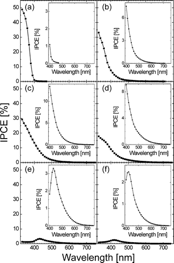 | ||
| Fig. 7 IPCE spectra recorded in LiClO4 (0.1 M) + KI (0.1 M) electrolyte at 0.5 V vs.Ag/AgCl for unmodified TiO2 (a) and TiO2–N modified at 300 °C (b), 350 °C (c), 400 °C (d), 450 °C (e), and 500 °C (f). The insets show zoomed plots in the visible light region. | ||
Two further important features of the IPCE spectra must be mentioned here. First, when one compares the IPCE values in the visible with the wavelengths corresponding to bandgap energies in Fig. 5 it becomes clear that all samples show significant sub-bandgap photocurrent response. This response is apparently due to excitation of electrons from the Urbach tail surface states which in TiO2–N reach down to ∼1.3 V vs.NHE (dashed area in Fig. 5) and, taking into account the positions of the conduction band edges, can therefore induce photocurrents upon irradiation by light with as low energy as ∼1.6–1.7 eV (∼750 nm). The second important feature of the IPCE spectra is the continuous decrease of IPCE values in the high-energy UV part of the spectrum with increasing modification temperature, i.e. with decreasing bandgap. In case of TiO2–N modified at 450 °C and 500 °C this results even in such a decrease of IPCE values in the UV that a maximum is generated at ∼420–430 nm. In general, a decrease in IPCE with increasing photon energy can be rationalized in terms of enhanced surface recombination.105 Since the absorption coefficient at short wavelengths increases, the penetration depth of light decreases. Thus, the absorption of light is more and more confined to a thin surface layer at each particle, which results in higher probability of surface recombination of photogenerated charges. As expected, the surface recombination in UV light is continuously enhanced with decreasing bandgap (i.e. with increased absorption; see Fig. 1 and 2) and results in the decrease of IPCE values in the high-energy part of the spectrum. Furthermore, decreasing the bandgap of the materials also leads to a situation where the short-wavelength light is almost utterly absorbed by particles in the very vicinity of the (backside-illuminated) ITO substrate, which will again inevitably lead to enhanced recombination due to local exhaustion of hole-scavenging species. In contrast, the light with longer wavelengths can penetrate deeper into the electrode and the light absorption and charge generation occurs thus in a larger volume. This might lead to lower recombination probability at longer wavelengths, which can finally result in the IPCE maximum peaks as observed in Fig. 7(e) and 7(f).
Conclusions
Surface-modification of nanocrystalline TiO2 by urea pyrolysis products at different temperatures can be used for tuning the fundamental optical and photoelectrochemical properties of titania. The modification process is based on incorporation of nitrogen species containing carbon into the surface structure of titania. With increasing modification temperature the optical bandgap of surface-modified TiO2 is continuously shifted down to ∼2.1 eV, which represents a bandgap narrowing by ∼1.1 eV as compared to unmodified TiO2. The anodic shift of the quasi-Fermi level of electrons from –0.6 V to –0.3 V vs.NHE is presumably related to partial reduction of surface Ti4+ and coincides well with the shift of the Ti2p3/2 XPS peak to lower binding energies. The new materials exhibit photocurrents in the visible down to 750 nm in accordance with the optical properties showing enhanced sub-bandgap absorption (Urbach tail). Maximum IPCE values were observed for the materials modified at 350 °C and 400 °C. The efficiency of photocurrent generation in surface-modified TiO2 seems to be limited by surface recombination, which leads to a significant decrease in IPCE values especially at shorter wavelengths. The effect of surface recombination becomes more pronounced with decreasing bandgap which makes itself manifest in remarkably different shapes of the IPCE spectra.Acknowledgements
We thank A. Friedrich for SEM analysis, M. Gärtner for synthesis of (DP)Br2, H. Hildebrand for XPS measurements, S. Hoffmann for XRD measurements, R. Müller for TGA analysis, S. Smolny for surface area measurements, C. Wronna for elemental analysis, M. Weller for construction of the photoelectrochemical cell, and D. Mitoraj for valuable discussions.Notes and references
- R. Memming, Semiconductor Electrochemistry, Wiley-VCH, Weinheim, 2001 Search PubMed.
- P. V. Kamat, Photochemistry on nonreactive and reactive (semiconductor) surfaces, Chem. Rev., 1993, 93, 267–300 CrossRef CAS.
- H. Kisch, Semiconductor photocatalysis for organic synthesis, Adv. Photochem., 2001, 26, 93–143 CAS.
- M. Gärtner, J. Ballmann, C. Damm, F. W. Heinemann and H. Kisch, Support-controlled chemoselective olefin-imine addition photocatalyzed by cadmium sulfide on a zinc sulfide carrier, Photochem. Photobiol. Sci., 2007, 6, 159–164 RSC.
- D. A. Tryk, A. Fujishima and K. Honda, Recent topics in photoelectrochemistry: achievements and future prospects, Electrochim. Acta, 2000, 45, 2363–2376 CrossRef CAS.
- K. Rajeshwar, N. R. de Tacconi and C. R. Chenthamarakshan, Semiconductor-Based Composite Materials: Preparation, Properties, and Performance, Chem. Mater., 2001, 13, 2765–2782 CrossRef CAS.
- M. Grätzel, Photoelectrochemical cells, Nature, 2001, 414, 338–344 CrossRef CAS.
- S. Licht, N. Myung and Y. Sun, A Light Addressable Photoelectrochemical Cyanide Sensor, Anal. Chem., 1996, 68, 954–959 CrossRef CAS.
- C. Stoll, S. Kudera, W. J. Parak and F. Lisdat, Quantum dots on gold: electrodes for photoswitchable cytochrome C electrochemistry, Small, 2006, 2, 741–743 CrossRef CAS.
- D. G. Wu, G. Ashkenasy, D. Shvarts, R. V. Ussyshkin, R. Naaman, A. Shanzer and D. Cahen, Novel NO biosensor based on the surface derivatization of GaAs by “hinged” iron porphyrins, Angew. Chem., Int. Ed., 2000, 39, 4496–4500 CrossRef CAS.
- D. G. Hafeman, J. W. Parce and H. M. McConnell, Light-addressable potentiometric sensor for biochemical systems, Science, 1988, 240, 1182–1185 CAS.
- I. Willner and B. Willner, Functional nanoparticle architectures for sensoric, optoelectronic, and bioelectronic applications, Pure Appl. Chem., 2002, 74, 1773–1783 CrossRef CAS.
- A. Vilan, A. Shanzer and D. Cahen, Molecular control over Au/GaAs diodes, Nature, 2000, 404, 166–168 CrossRef CAS.
- R. Cohen, S. Bastide, D. Cahen, J. Libman, A. Shanzer and Y. Rosenwaks, Controlling surfaces and interfaces of semiconductors using organic molecules, Opt. Mater., 1998, 9, 394–400 CrossRef CAS.
- D. Bonifazi, A. Salomon, O. Enger, F. Diederich and D. Cahen, Tuning electronic properties of semiconductors by adsorption of [60] fullerene carboxylic acid derivatives, Adv. Mater., 2002, 14, 802–805 CrossRef CAS.
- S. P. Wilks, Engineering and investigating the control of semiconductor surfaces and interfaces, J. Phys. D: Appl. Phys., 2002, 35, R77–R90 CrossRef CAS.
- M. Anpo, Use of visible light. Second-generation titanium oxide photocatalysts prepared by the application of an advanced metal ion-implantation method, Pure Appl. Chem., 2000, 72, 1787–1792 CrossRef CAS.
- H. Weiss, A. Fernandez and H. Kisch, Electronic semiconductor-support interaction - a novel effect in semiconductor photocatalysis, Angew. Chem., Int. Ed., 2001, 40, 3825–3827 CrossRef.
- M. Gärtner, V. Dremov, P. Mueller and H. Kisch, Bandgap widening of titania through semiconductor support interactions, ChemPhysChem, 2005, 6, 714–718 CrossRef CAS.
- M. R. Hoffmann, S. T. Martin, W. Choi and D. W. Bahnemann, Environmental Applications of Semiconductor Photocatalysis, Chem. Rev., 1995, 95, 69–96 CrossRef CAS.
- A. Fujishima, T. N. Rao and D. A. Tryk, Titanium dioxide photocatalysis, J. Photochem. Photobiol., C, 2000, 1, 1–21 CrossRef CAS.
- O. Carp, C. L. Huisman and A. Reller, Photoinduced reactivity of titanium dioxide, Prog. Solid State Chem., 2004, 32, 33–177 CrossRef CAS.
- A. L. Linsebigler, G. Lu and J. T. Yates, Jr., Photocatalysis on TiO2 Surfaces: Principles, Mechanisms, and Selected Results, Chem. Rev., 1995, 95, 735–758 CrossRef CAS.
- T. L. Thompson and J. T. Yates, Jr., TiO2-based photocatalysis: Surface defects, oxygen and charge transfer, Top. Catal., 2005, 35, 197–210 CrossRef CAS.
- H. Gerischer and H. Tributsch, Electrochemical studies on the spectral sensitization of zinc oxide single crystals, Ber. Bunsen-Ges. Phys. Chem., 1968, 72, 437–445 CAS.
- B. O'Regan and M. Grätzel, A low-cost, high-efficiency solar cell based on dye-sensitized colloidal titanium dioxide films, Nature, 1991, 353, 737–740 CrossRef CAS.
- H. Kisch, L. Zang, C. Lange, W. F. Maier, C. Antonius and D. Meissner, Heterogeneous photocatalysis. Part 18. Modified, amorphous titania - a hybrid semiconductor for detoxification and current generation by visible light, Angew. Chem., Int. Ed., 1998, 37, 3034–3036 CrossRef CAS.
- H. Kisch, G. Burgeth and W. Macyk, Visible light photocatalysis by a titania transition metal complex, Adv. Inorg. Chem., 2004, 56, 241–259 CAS.
- R. Vogel, P. Hoyer and H. Weller, Quantum-Sized PbS, CdS, Ag2S, Sb2S3, and Bi2S3 Particles as Sensitizers for Various Nanoporous Wide-Bandgap Semiconductors, J. Phys. Chem., 1994, 98, 3183–3188 CrossRef CAS.
- A. J. Nozik, Quantum dot solar cells, Physica E, 2002, 14, 115–120 CrossRef CAS.
- L. M. Peter, D. J. Riley, E. J. Tull and K. G. U. Wijayantha, Photosensitization of nanocrystalline TiO2 by self-assembled layers of CdS quantum dots, Chem. Commun., 2002, 1030–1031 RSC.
- L. Palmisano, V. Augugliaro, A. Sclafani and M. Schiavello, Activity of chromium-ion-doped titania for the dinitrogen photoreduction to ammonia and for the phenol photodegradation, J. Phys. Chem., 1988, 92, 6710–6713 CrossRef.
- A. Di Paola, G. Marci, L. Palmisano, M. Schiavello, K. Uosaki, S. Ikeda and B. Ohtani, Preparation of Polycrystalline TiO2 Photocatalysts Impregnated with Various Transition Metal Ions: Characterization and Photocatalytic Activity for the Degradation of 4-Nitrophenol, J. Phys. Chem. B, 2002, 106, 637–645 CrossRef.
- C. Lettmann, K. Hildenbrand, H. Kisch, W. Macyk and W. F. Maier, Visible light photodegradation of 4-chlorophenol with a coke-containing titanium dioxide photocatalyst, Appl. Catal., B, 2001, 32, 215–227 CrossRef CAS.
- S. U. M. Khan, M. Al-Shahry and W. B. Ingler, Jr., Efficient photochemical water splitting by a chemically modified n-TiO2, Science, 2002, 297, 2243–2245 CrossRef CAS.
- S. Sakthivel and H. Kisch, Daylight photocatalysis by carbon-modified titanium dioxide, Angew. Chem., Int. Ed., 2003, 42, 4908–4911 CrossRef CAS.
- C. S. Enache, J. Schoonman and R. van de Krol, Addition of carbon to anatase TiO2 by n-hexane treatment-surface or bulk doping?, Appl. Surf. Sci., 2006, 252, 6342–6347 CrossRef CAS.
- M. Janus, B. Tryba, M. Inagaki and A. W. Morawski, New preparation of a carbon-TiO2 photocatalyst by carbonization of n-hexane deposited on TiO2, Appl. Catal., B, 2004, 52, 61–67 CrossRef CAS.
- T. Hirai, I. Tari and J. Yamaura, Titanium nitride oxide (TiN0.07O1.93) semiconductor electrodes for photoassisted oxidation of water, Bull. Chem. Soc. Jpn., 1978, 51, 3057–3058 CrossRef CAS.
- S. Sato, Photocatalytic activity of nitrogen oxide (NOx)-doped titanium dioxide in the visible light region, Chem. Phys. Lett., 1986, 123, 126–128 CrossRef CAS.
- R. Asahi, T. Morikawa, T. Ohwaki, K. Aoki and Y. Taga, Visible-light photocatalysis in nitrogen-doped titanium oxides, Science, 2001, 293, 269–271 CrossRef CAS.
- S. Sakthivel and H. Kisch, Photocatalytic and photoelectrochemical properties of nitrogen-doped titanium dioxide, ChemPhysChem, 2003, 4, 487–490 CrossRef CAS.
- S. Sakthivel, M. Janczarek and H. Kisch, Visible Light Activity and Photoelectrochemical Properties of Nitrogen-Doped TiO2, J. Phys. Chem. B, 2004, 108, 19384–19387 CrossRef CAS.
- T. Lindgren, J. M. Mwabora, E. Avendano, J. Jonsson, A. Hoel, C.-G. Granqvist and S.-E. Lindquist, Photoelectrochemical and Optical Properties of Nitrogen Doped Titanium Dioxide Films Prepared by Reactive DC Magnetron Sputtering, J. Phys. Chem. B, 2003, 107, 5709–5716 CrossRef CAS.
- H. Irie, Y. Watanabe and K. Hashimoto, Nitrogen-Concentration Dependence on Photocatalytic Activity of TiO2–xNx Powders, J. Phys. Chem. B, 2003, 107, 5483–5486 CrossRef CAS.
- C. Burda, Y. Lou, X. Chen, A. C. S. Samia, J. Stout and J. L. Gole, Enhanced Nitrogen Doping in TiO2 Nanoparticles, Nano Lett., 2003, 3, 1049–1051 CrossRef CAS.
- M. Sathish, B. Viswanathan, R. P. Viswanath and C. S. Gopinath, Synthesis, Characterization, Electronic Structure, and Photocatalytic Activity of Nitrogen-Doped TiO2 Nanocatalyst, Chem. Mater., 2005, 17, 6349–6353 CrossRef CAS.
- T. Umebayashi, T. Yamaki, H. Itoh and K. Asai, Band gap narrowing of titanium dioxide by sulfur doping, Appl. Phys. Lett., 2002, 81, 454–456 CrossRef CAS.
- T. Ohno, Preparation of visible light active S-doped TiO2 photocatalysts and their photocatalytic activities, Water Sci. Technol., 2004, 49, 159–163 Search PubMed.
- Y. Nakano, T. Morikawa, T. Ohwaki and Y. Taga, Band-gap narrowing of TiO2 films induced by N-doping, Physica B, 2006, 376–377, 823–826 CrossRef CAS.
- J. L. Gole, J. D. Stout, C. Burda, Y. Lou and X. Chen, Highly Efficient Formation of Visible Light Tunable TiO2-xNx Photocatalysts and Their Transformation at the Nanoscale, J. Phys. Chem. B, 2004, 108, 1230–1240 CrossRef CAS.
- S. Yin, Q. Zhang, F. Saito and T. Sato, Preparation of visible light-activated titania photocatalyst by mechanochemical method, Chem. Lett., 2003, 32, 358–359 CrossRef CAS.
- H. Irie, S. Washizuka, Y. Watanabe, T. Kako and K. Hashimoto, Photoinduced hydrophilic and electrochemical properties of nitrogen-doped TiO2 films, J. Electrochem. Soc., 2005, 152, E351–E356 CrossRef.
- O. Diwald, T. L. Thompson, E. G. Goralski, S. D. Walck and J. T. Yates, Jr., The Effect of Nitrogen Ion Implantation on the Photoactivity of TiO2 Rutile Single Crystals, J. Phys. Chem. B, 2004, 108, 52–57 CrossRef CAS.
- A. Ghicov, J. M. Macak, H. Tsuchiya, J. Kunze, V. Haeublein, L. Frey and P. Schmuki, Ion Implantation and Annealing for an Efficient N-Doping of TiO2 Nanotubes, Nano Lett., 2006, 6, 1080–1082 CrossRef CAS.
- Y. Nosaka, M. Matsushita, J. Nishino and A. Y. Nosaka, Nitrogen-doped titanium dioxide photocatalysts for visible response prepared by using organic compounds, Sci. Tech. Adv. Mater., 2005, 6, 143–148 Search PubMed.
- H. Kisch, S. Sakthivel, M. Janczarek and D. Mitoraj, A Low-Band Gap, Nitrogen-Modified Titania Visible-Light Photocatalyst, J. Phys. Chem. C, 2007, 111, 11445–11449 CrossRef CAS.
- C. S. Gopinath, Comment on “Photoelectron Spectroscopic Investigation of Nitrogen-Doped Titania Nanoparticles, J. Phys. Chem. B, 2006, 110, 7079–7080 CrossRef CAS.
- C. Burda and J. Gole, Reply to “Comment on ‘Photoelectron Spectroscopic Investigation of Nitrogen-Doped Titania Nanoparticles’“, J. Phys. Chem. B, 2006, 110, 7081–7082 CrossRef CAS.
- O. Diwald, T. L. Thompson, T. Zubkov, E. G. Goralski, S. D. Walck and J. T. Yates, Jr., Photochemical Activity of Nitrogen-Doped Rutile TiO2(110) in Visible Light, J. Phys. Chem. B, 2004, 108, 6004–6008 CrossRef CAS.
- S. M. Prokes, J. L. Gole, X. Chen, C. Burda and W. E. Carlos, Defect-related optical behavior in surface-modified TiO2 nanostructures, Adv. Funct. Mater., 2005, 15, 161–167 CrossRef CAS.
- X. Chen, Y. Lou, A. C. S. Samia, C. Burda and J. L. Gole, Formation of oxynitride as the photocatalytic enhancing site in nitrogen-doped titania nanocatalysts: comparison to a commercial nanopowder, Adv. Funct. Mater., 2005, 15, 41–49 CrossRef CAS.
- C. Di Valentin, G. Pacchioni, A. Selloni, S. Livraghi and E. Giamello, Characterization of Paramagnetic Species in N-Doped TiO2 Powders by EPR Spectroscopy and DFT Calculations, J. Phys. Chem. B, 2005, 109, 11414–11419 CrossRef CAS.
- N. Serpone, Is the Band Gap of Pristine TiO2 Narrowed by Anion- and Cation-Doping of Titanium Dioxide in Second-Generation Photocatalysts?, J. Phys. Chem. B, 2006, 110, 24287–24293 CrossRef CAS; A. V. Emeline, N. V. Sheremetyeva, N. V. Khomchenko, V. K. Ryabchuk and N. Serpone, Photoinduced Formation of Defects and Nitrogen Stabilization of Color Centers in N-Doped Titanium Dioxide, J. Phys. Chem. C, 2007, 111, 11456–11462 CrossRef CAS.
- R. Beranek and H. Kisch, Surface-modified anodic TiO2 films for visible light photocurrent response, Electrochem. Commun., 2007, 9, 761–766 CrossRef CAS.
- G. R. Torres, T. Lindgren, J. Lu, C.-G. Granqvist and S.-E. Lindquist, Photoelectrochemical Study of Nitrogen-Doped Titanium Dioxide for Water Oxidation, J. Phys. Chem. B, 2004, 108, 5995–6003 CrossRef CAS.
- T. Lindgren, J. Lu, A. Hoel, C.-G. Granqvist, G. R. Torres and S.-E. Lindquist, Photoelectrochemical study of sputtered nitrogen-doped titanium dioxide thin films in aqueous electrolyte, Sol. Energy Mater. Sol. Cells, 2004, 84, 145–157 CrossRef CAS.
- R. Nakamura, T. Tanaka and Y. Nakato, Mechanism for Visible Light Responses in Anodic Photocurrents at N-Doped TiO2 Film Electrodes, J. Phys. Chem. B, 2004, 108, 10617–10620 CrossRef CAS.
- R. P. Vitiello, J. M. Macak, A. Ghicov, H. Tsuchiya, L. F. P. Dick and P. Schmuki, N-Doping of anodic TiO2 nanotubes using heat treatment in ammonia, Electrochem. Commun., 2006, 8, 544–548 CrossRef CAS.
- M. Batzill, E. H. Morales and U. Diebold, Influence of Nitrogen Doping on the Defect Formation and Surface Properties of TiO2 Rutile and Anatase, Phys. Rev. Lett., 2006, 96, 026103 CrossRef.
- S. Livraghi, M. C. Paganini, E. Giamello, A. Selloni, C. Di, Valentin and G. Pacchioni, Origin of Photoactivity of Nitrogen-Doped Titanium Dioxide under Visible Light, J. Am. Chem. Soc., 2006, 128, 15666–15671 CrossRef CAS.
- Y. Nakano, T. Morikawa, T. Ohwaki and Y. Taga, Deep-level optical spectroscopy investigation of N-doped TiO2 films, Appl. Phys. Lett., 2005, 86, 132104 CrossRef.
- J.-Y. Lee, J. Park and J.-H. Cho, Electronic properties of N- and C-doped TiO2, Appl. Phys. Lett., 2005, 87, 011904 CrossRef.
- A. M. Roy, G. C. De, N. Sasmal and S. S. Bhattacharyya, Determination of the flatband potential of semiconductor particles in suspension by photovoltage measurement, Int. J. Hydrogen Energy, 1995, 20, 627–630 CrossRef CAS.
- H. Lindstrom, E. Magnusson, A. Holmberg, S. Sodergren, S.-E. Lindquist and A. Hagfeldt, A new method for manufacturing nanostructured electrodes on glass substrates, Sol. Energy Mater. Sol. Cells, 2002, 73, 91–101 CrossRef.
- W. W. Wendlandt and H. G. Hecht, in Chemical Analysis, ed. P. J. Elving and I. M. Kolthoff, Interscience, New York, 1966, vol. 21, p. 298 Search PubMed.
- J. I. Pankove, Optical Processes in Semiconductors, Prentience-Hall Inc., New Jersey, 1971 Search PubMed.
- H. Tang, K. Prasad, R. Sanilines, P. E. Schmid and F. Levy, Electrical and optical properties of TiO2 anatase thin films, J. Appl. Phys., 1994, 75, 2042–2047 CrossRef CAS.
- H. Tang, F. Levy, H. Berger and P. E. Schmid, Urbach tail of anatase TiO2, Phys. Rev. B: Condens. Matter, 1995, 52, 7771–7774 CrossRef CAS.
- T. Dittrich, Porous TiO2: electron transport and application to dye sensitized injection solar cells, Phys. Status Solidi A, 2000, 182, 447–455 CrossRef CAS.
- V. Duzhko, V. Y. Timoshenko, F. Koch and T. Dittrich, Photovoltage in nanocrystalline porous TiO2, Phys. Rev. B: Condens. Matter Mater. Phys., 2001, 64, 075204 CrossRef.
- P. M. Schaber, J. Colson, S. Higgins, D. Thielen, B. Anspach and J. Brauer, Thermal decomposition (pyrolysis) of urea in an open reaction vessel, Thermochim. Acta, 2004, 424, 131–142 CrossRef CAS.
- The content of Ti was calculated by subtracting the content of C, N, O and H obtained from elemental analysis.
- T. Morikawa, R. Asahi, T. Ohwaki, K. Aoki and Y. Taga, Band-gap narrowing of titanium dioxide by nitrogen doping, Jpn. J. Appl. Phys., Part 2, 2001, 40, L561–L563 CrossRef CAS.
- H. Irie, S. Washizuka, N. Yoshino and K. Hashimoto, Visible-light induced hydrophilicity on nitrogen-substituted titanium dioxide films, Chem. Commun., 2003, 1298–1299 RSC.
- A. P. Dementjev, A. De Graaf, M. C. M. Van, de Sanden, K. I. Maslakov, A. V. Naumkin and A. A. Serov, X-ray photoelectron spectroscopy reference data for identification of the C3N4 phase in carbon-nitrogen films, Diamond Relat. Mater., 2000, 9, 1904–1907 CrossRef CAS.
- Q. Guo, Y. Xie, X. Wang, S. Zhang, T. Hou and S. Lu, Synthesis of carbon nitride nanotubes with the C3N4 stoichiometry via a benzene-thermal process at low temperatures, Chem. Commun., 2004, 26–27 RSC.
- C. Zhao, L. Ji, H. Liu, G. Hu, S. Zhang, M. Yang and Z. Yang, Functionalized carbon nanotubes containing isocyanate groups, J. Solid State Chem., 2004, 177, 4394–4398 CrossRef CAS.
- S. Livraghi, A. Votta, M. C. Paganini and E. Giamello, The nature of paramagnetic species in nitrogen doped TiO2 active in visible light photocatalysis, Chem. Commun., 2005, 498–500 RSC.
- F. P. Larkins and A. Lubenfeld, The Auger spectrum of solid ammonia, J. Electron Spectrosc. Relat. Phenom., 1979, 15, 137–144 CrossRef CAS.
- U. Bardi, K. Tamura, M. Owari and Y. Nihei, Angular resolved X-ray photoemission study of defects induced by ion bombardment on the titania surface, Appl. Surf. Sci., 1988, 32, 352–362 CrossRef CAS.
- J. T. Mayer, U. Diebold, T. E. Madey and E. Garfunkel, Titanium and reduced titania overlayers on titanium dioxide(110), J. Electron Spectrosc. Relat. Phenom., 1995, 73, 1–11 CrossRef CAS.
- N. C. Saha and H. G. Tompkins, Titanium nitride oxidation chemistry: an X-ray photoelectron spectroscopy study, J. Appl. Phys., 1992, 72, 3072–3079 CrossRef CAS.
- W. Göpel, J. A. Anderson, D. Frankel, M. Jaehnig, K. Phillips, J. A. Schaefer and G. Rocker, Surface defects of titanium dioxide(110): a combined XPS, XAES and ELS study, Surf. Sci., 1984, 139, 333–346 CrossRef.
- R. Beranek, B. Neumann, S. Sakthivel, M. Janczarek, T. Dittrich, H. Tributsch and H. Kisch, Exploring the Electronic Structure of Nitrogen-Modified TiO2 Photocatalysts through Photocurrent and Surface Photovoltage Studies, Chem. Phys., 2007, 339, 11–19 CrossRef CAS.
- S. R. Morrison, Electrochemistry at Semiconductor and Oxidized Metal Electrodes, Plenum Press, New York, 1980 Search PubMed.
- L. Kavan, M. Grätzel, S. E. Gilbert, C. Klemenz and H. J. Scheel, Electrochemical and photoelectrochemical investigation of single-crystal anatase, J. Am. Chem. Soc., 1996, 118, 6716–6723 CrossRef CAS.
- A. J. Bard, Design of semiconductor photoelectrochemical systems for solar energy conversion, J. Phys. Chem., 1982, 86, 172–177 CrossRef CAS.
- A. Hagfeldt and M. Grätzel, Light-Induced Redox Reactions in Nanocrystalline Systems, Chem. Rev., 1995, 95, 49–68 CrossRef CAS.
- G. Hodes, I. D. J. Howell and L. M. Peter, Nanocrystalline photoelectrochemical cells. A new concept in photovoltaic cells, J. Electrochem. Soc., 1992, 139, 3136–3140 CAS.
- A. Wahl, M. Ulmann, A. Carroy and J. Augustynski, Highly selective photo-oxidation reactions at nanocrystalline TiO2 film electrodes, J. Chem. Soc., Chem. Commun., 1994, 2277–2278 RSC.
- J. J. Kelly and D. Vanmaekelbergh, Charge carrier dynamics in nanoporous photoelectrodes, Electrochim. Acta, 1998, 43, 2773–2780 CrossRef CAS.
- R. Solarska, I. Rutkowska, R. Morand and J. Augustynski, Photoanodic reactions occurring at nanostructured titanium dioxide films, Electrochim. Acta, 2006, 51, 2230–2236 CrossRef CAS.
- P. Wardman, Reduction potentials of one-electron couples involving free radicals in aqueous solution, J. Phys. Chem. Ref. Data, 1989, 18, 1637–1755 CAS.
- It is noted that the change in transmission properties of ITO-glass was negligible upon modification at different temperatures.
Footnote |
| † Electronic supplementary information (ESI) available: X-Ray diffractometry patterns; FT-IR spectra; thermogravimetry data; details for removal of modification in boiling NaOH; details for Ti2p XPS upon sputtering; influence of the starting material properties on the modification; graphs of quasi-Fermi level measurements; raw photocurrent spectra without and with addition of iodide. See DOI: 10.1039/b711658f |
| This journal is © The Royal Society of Chemistry and Owner Societies 2008 |