Nanochannels in SU-8 with floor and ceiling metal electrodes and integrated microchannels†
Kevin P.
Nichols
*a,
Jan C. T.
Eijkel
b and
Han J. G. E.
Gardeniers
a
aMesoscale Chemical Systems, MESA+ Institute for Nanotechnology, University of Twente, Postbus 217, 7500 AE Enschede, The Netherlands. E-mail: k.p.nichols@utwente.nl; Tel: +31-53-489-2631
bBIOS, The Lab on a Chip Group, MESA+ Institute for Nanotechnology, University of Twente, Postbus 217, 7500 AE Enschede, The Netherlands
First published on 8th November 2007
Abstract
Sacrificially etched 2-D nanofluidic channels and nanospaces with integrated floor and ceiling electrodes and arbitrary channel geometries have been demonstrated with channel heights from 20 nm to 400 nm, widths from 800 nm to 40 µm, and lengths up to 3 mm, using SU-8 as the channel structural material.
Introduction
Nanochannels are channels with at least one dimension in the nanometre range.1 A variety of top-down and bottom-up approaches for nanochannel fabrication have been reported.1–5 Here, we present a technique for the fabrication of nanochannels and nanospaces in SU-8, a commonly used, photo-definable epoxy for microelectromechanical systems (MEMS) devices, with integrated floor and ceiling electrodes.Much attention has been focused on the benefits that accrue from very small working electrodes in electrochemical systems, where electron transfer to the electrode surface is less likely to be limited by mass transport.6–8 Further applications for integrated electrodes in nanochannels may include surface functionalization with DNA and proteins,9,10 fluidic control in nanochannels,11surface enhanced Raman scattering (SERS),12–14 and single molecule studies15 of large molecules such as DNA.
Adhesion of the metal layers in a nanochannel system with floor and ceiling electrodes is a significant problem that we have demonstrated can be overcome using SU-8 or SU-8 3000. Additionally, utilizing SU-8 allows for direct integration with SU-8 based MEMS and microfluidics; simple patterning of interconnections due to the photo-definable nature of SU-8;16 sufficiently thick channel roofs to prevent bending due to capillarity induced negative pressure, as has previously been problematic;17 and arbitrary nanochannel geometries due to the conformal nature of SU-8 dispensing.
Nanochannels have previously demonstrated utility in fundamental studies of liquid behavior,18 single molecule analysis,19–22 single cell analysis,23 and in other studies where surface phenomena dominate over bulk phenomena.2
Experimental
Nanochannel fabrication
Fabrication of the device followed standard photolithography procedures. A sequence of metal layers was deposited on a substrate such that the bottom and top layers were usable as electrodes, and the middle layer could be sacrificially removed without affecting the electrode layers. The substrate was then coated with SU-8 (Microchem, USA) to provide the lid of the nanochannel along with fluidic inlets and outlets. Finally, the sacrificial layer was removed. Since the nanochannel structural material is SU-8, if this is patterned, microchannels or reservoirs can be directly included. If a lid for these microchannels is required, glass or PDMS can be easily bonded. Simple nanochannels without electrodes were also constructed using only a patterned sacrificial layer.An overview is presented in Fig. 1. In step 1, the top and bottom electrode were defined on a Si substrate, along with the sacrificial layer between the electrodes. Metallization was accomplished using a custom built sputtering tool, though most common metallization tools should produce equivalent results. Metal stacks were deposited without breaking vacuum. A wide variety of electrode/sacrificial layers are possible (Table 1). As an example, the channels in Fig. 2 were fabricated using a stack of Ta/Au/Cr/Au with heights of 20 nm, 100 nm, 100 nm and 100 nm respectively, deposited by sputtering. For galvanically coupled metals, care should be taken to design the photoresist masks to minimize the total etched area, since underetching will be significantly accelerated if large metal areas are exposed. Additionally, the top and bottom metal layers must be underetched relative to the sacrificial layer, to prevent short circuits. Previous work has demonstrated good adhesion of SU-8 to a variety of metal layers.24
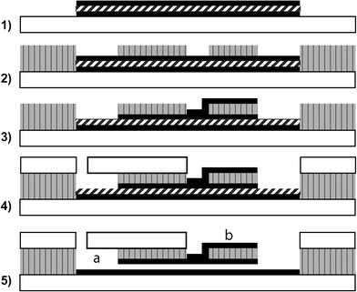 | ||
| Fig. 1 Process for SU-8 nanofluidic channel with top/bottom electrodes and integrated microchannels. (1) Top electrode, bottom electrode (black, solid) and sacrificial layer (thick black slanted line) patterned. (2) SU-8 (gray, vertical black lines) patterned with microchannels and electrode access holes/vias. (3) Metal layer sputtered for contact pads and contact with top electrode. (4) Patterned glass or PDMS bonded to structural SU-8. (5) Sacrificial layer removed, (a) represents a microchannel (running into the plane) or a contact pad for the bottom electrode, (b) represents the top electrode contact pad. The bottom electrode contact pad and the microchannels are shown colocated, though this is not necessary. The via to the left of (b) must be small enough at the bottom such that the metal membrane will not significantly deflect, or an additional layer of SU-8 must be used as a structural support. | ||
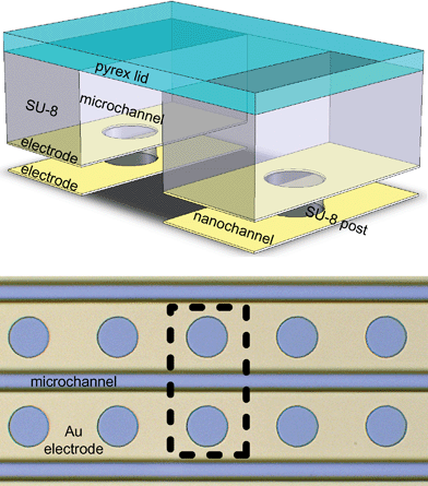 | ||
| Fig. 2 The top image shows a drawing (not to scale) of a glass covered (plate on top) SU-8 microchannel (center of drawing, SU-8 shown by rectangles and pillars), and nanochannels (gaps under SU-8 walls) with Au electrodes. The circles in the electrode layers allow posts of SU-8 to support the structure. The bottom image is a micrograph of such a system viewed from above, with the area shown in the top image indicated by the dashed line. The electrode layer is in focus. | ||
In step 2, a single layer of SU-8 was dispensed to a thickness of 15 µm and patterned to create microfluidic channels and access to the top and bottom electrodes. Standard manufacturer recommended processing was used.
In step 3, an additional metal layer was sputtered and patterned to create contact pads and electrical contacts with the top electrode. This layer should be sputtered at a pressure sufficient to ensure good step coverage. We obtained sufficient step coverage at 1 × 10⁻² bar. Ideally, this via should be small enough at the bottom such that insignificant deflection of the metal membrane occurs, and no additional support is needed. However, this requires careful tuning specific to the device, equipment, and surface reflectivity. If not initially practical, an additional SU-8 layer can be used to support the thin metal membrane.
In step 4, the microchannels that connect to the nanochannels are sealed using a patterned glass or PDMS lid. Standard PDMS processing can be used for PDMS lids. For glass lids, holes were etched using powder blasting, and bonding was achieved using a simple office laminator set to 150 °C. Interconnections with glass and PDMS lids have been well documented elsewhere.
Before sacrificial etching, it is important to once again expose and bake the SU-8 device for at least three times the recommended exposure time. For short channels that require minutes to hours of etching, this is less critical.
In step 5, the sacrificial layer was removed. Cr was etched in BASF Selectipur Chromium Etch, an ammonium cerium(IV) nitrate based etchant. Au was etched in KI : I2 : DI = 4 : 1 : 40. Etching within channels is limited by diffusion, and thus will be highly dependent on device geometry. Certain metal combinations will result in galvanic coupling that will significantly affect etch rates.25 Calibration for a specific system is possible by monitoring the impedance across the electrodes, as the etch proceeds.
We achieved equivalent results with SU-8, and the newer SU-8 3000 series, a version of SU-8 formulated in a solvent specifically designed to improve adhesion. The major difference was in yield; SU-8 3000 was far less sensitive to fouling of the metal surfaces. SU-8 2000 was not investigated.
Integration with microfluidic channels
Since the nanochannel structural material is SU-8, microchannels can be patterned in a single lithographic step. A variety of alternative designs could easily be constructed, such as interdigitated microchannels with nanochannels connecting the two sides. A lid can be attached to the SU-8 microchannels by bonding a patterned piece of glass26 or PDMS.27Channel geometries
Simple electrode geometries with planar channels can be constructed in a single lithography step. More complicated geometries require an additional step to define the electrodes/channel independently. For example, a channel with grooves could be constructed using two steps instead of the single step shown in Fig. 1, step 1. Any arbitrary structure that can be lithographically patterned can be used to define the nanochannels.Nanochannels with widths from 800 nm to 40 µm were fabricated. Channels with widths below 1 µm can be fabricated using e-beam lithography, or more advanced photolithography techniques. Channels with widths above 40 µm should be avoided due to channel collapse. For wide structures, pillars may be placed every 40 µm or less to extend the device's width (Fig. 2). Channels with heights from 20 nm to 400 nm were fabricated.
Stability of SU-8 in various etchants
SU-8 is a highly functionalized epoxy; removal typically requires harsh etchants or plasma treatments.28 Nonetheless, some slow dissolution will occur. To measure these slow etch rates, a thick grid pattern was fabricated on an SU-8 surface. For Au etchant testing and Cr etchant testing, a 1 µm thick Pyrex mask was sputtered using a Nordiko NM2000 (Nordiko, UK) onto an unpatterned, fully crosslinked SU-8 substrate, and was subsequently patterned in BHF using a Cr mask. For BHF testing, a 500 nm Cr mask was sputtered using a custom sputtering tool. Subsequently, etching experiments were conducted, the mask was removed, and an AFM scan (Digital Instruments Nanoscope III, Veeco, USA) was used to determine the relative SU-8 height before and after etching. Testing as described above revealed SU-8 etch rates in BASF Selectipur Chromium Etch to be less than 2 nm day–1, and in BHF to be less than 1 nm day–1. SU-8 etch rates in KI : I2 : DI = 4 : 1 : 40 (Au etchant) were too low to be measurable. It is important to note that this testing is only valid for SU-8 that has been crosslinked far in excess of the recommended exposure times. High resolution is still achievable in these substrates however, as the resist can be exposed normally, developed, and then reexposed to improve cross-linking.Metal layer surface roughness
All metal–etchant combinations marked as “+” in Table 1 were measured using a Digital Instruments Nanoscope III (Veeco Inc., USA) to determine the surface roughness of the thin films before and after etching (Table 2). Measurements were made on metallized, but unpatterned Si wafers (bare wafers without SU-8 structuring, or sacrificial layer removal) before and after 24 h exposure to the indicated etchants. The wafers were annealed at 95 °C for 15 min to simulate processing.| Cr | Au | Ti | Ti/W | ITO | Pt | Cu | Ta | |
|---|---|---|---|---|---|---|---|---|
| Cr Etcha | — | 2.8 | — | — | — | 1.2 | — | 0.4 |
| 2.6 | 3.7 | 3.9 | ||||||
| Au Etchb | 1.5 | — | 0.9 | 0.4 | 0.7 | 1.2 | — | 0.4 |
| 1.4 | 0.6 | 0.8 | 3.0 | 1.2 | 0.3 | |||
| BHF | 1.5 | 2.8 | — | — | — | 1.2 | 5.2 | — |
| 3.9 | 1.0 | 9.8 | 4.9 |
Channel hydrophobicity
The hydrophobic–hydrophilic combination of the SU-8 nanochannel on a Si or Pyrex substrate (without electrodes) spontaneously fills with both DI water and Octane. Metallized nanochannels will fill dependent on the surface properties of the metal.Acknowledgements
This research was financially supported by the Technology Foundation STW, applied science division of NWO and the technology program of the Ministry of Economic Affairs of The Netherlands (project no. 6626).References
- J. C. T. Eijkel, J. Bomer, N. R. Tas and A. van den Berg, Lab Chip, 2004, 4, 161–163 RSC.
- D. Mijatovic, J. C. T. Eijkel and A. Van Den Berg, Lab Chip, 2005, 5, 492–500 RSC.
- M. B. Stern, M. W. Geis and J. E. Curtin, J. Vac. Sci. Technol., B: Microelectron. Nanometer Struct.–Process., Meas., Phenom., 1997, 15, 2887 Search PubMed.
- B. Ilic, D. Czaplewski, M. Zalalutdinov, B. Schmidt and H. G. Craighead, J. Vac. Sci. Technol., B: Microelectron. Nanometer Struct.–Process., Meas., Phenom., 2002, 20, 2459 Search PubMed.
- W. J. Nam, S. Bae, A. K. Kalkan and S. J. Fonash, J. Vac. Sci. Technol., A, 2001, 19, 1229 CrossRef CAS.
- D. W. M. Arrigan, Analyst, 2004, 129, 1157–1165 RSC.
- M. Pumera, S. Sanchez, I. Ichinose and J. Tang, Sens. Actuators, B, 2007, 123, 1195–1205 CrossRef.
- A. J. Bard, F. R. F. Fan, J. Kwak and O. Lev, Anal. Chem., 1989, 61, 132–138 CrossRef CAS.
- B. X. Ge, Y. C. Huang, D. Sen and H. Z. Yu, J. Electroanal. Chem., 2007, 602, 156–162 CrossRef CAS.
- A. Calzolari and R. Di Felice, J. Phys.: Condens. Matter, 2007, 19, 305018–305028 CrossRef.
- R. B. M. Schasfoort, S. Schlautmann, L. Hendrikse and A. van den Berg, Science, 1999, 286, 942–945 CrossRef CAS.
- P. Olk, J. Renger, T. Hartling, M. T. Wenzel and L. M. Eng, Nano Lett., 2007, 7, 1736–1740 CrossRef CAS.
- X. Wang, Y. Cui and B. Ren, Chemical Journal of Chinese Universities-Chinese, 2007, 28, 522–525 Search PubMed.
- S. W. Bishnoi, C. J. Rozell, C. S. Levin, M. K. Gheith, B. R. Johnson, D. H. Johnson and N. J. Halas, Nano Lett., 2006, 6, 1687–1692 CrossRef CAS.
- B. Q. Xu and N. J. J. Tao, Science, 2003, 301, 1221–1223 CrossRef CAS.
- G. J. Cheng, D. Pirzada and P. Dutta, J. Microlithogr. Microfabr. Microsyst., 2005, 4, 013009 Search PubMed.
- N. R. Tas, P. Mela, T. Kramer, J. W. Berenschot and A. van den Berg, Nano Lett., 2003, 3, 1537–1540 CrossRef CAS.
- A. Hibara, T. Saito, H. B. Kim, M. Tokeshi, T. Ooi, M. Nakao and T. Kitamori, Anal. Chem., 2002, 74, 6170–6176 CrossRef CAS.
- J. O. Tegenfeldt, C. Prinz, H. Cao, S. Chou, W. W. Reisner, R. Riehn, Y. M. Wang, E. C. Cox, J. C. Sturm and P. Silberzan, Proc. Natl. Acad. Sci. U. S. A., 2004, 101, 10979–10983 CrossRef CAS.
- S. S. Verbridge, J. B. Edel, S. M. Stavis, J. M. Moran-Mirabal, S. D. Allen, G. Coates and H. G. Craighead, J. Appl. Phys., 2005, 97, 124317 CrossRef.
- L. C. Campbell, M. J. Wilkinson, A. Manz, P. Camilleri and C. J. Humphreys, Lab Chip, 2004, 4, 225–229 RSC.
- H. Craighead, Nature, 2006, 442, 387–393 CrossRef CAS.
- H. Andersson and A. van den Berg, Curr. Opin. Biotechnol., 2004, 15, 44–49 CrossRef CAS.
- M. Nordstrom, A. Johansson, E. S. Nogueron, B. Clausen, M. Calleja and A. Boisen, Microelectron. Eng., 2005, 78–79, 152–157 CrossRef.
- P. R. Roberge, Handbook of Corrosion Engineering, McGraw-Hill Professional, New York, 1999 Search PubMed.
- F. J. Blanco, M. Agirregabiria, J. Garcia, J. Berganzo, M. Tijero, M. T. Arroyo, J. M. Ruano, I. Aramburu and K. Mayora, J. Micromech. Microeng., 2004, 14, 1047–1056 CrossRef.
- L. S. Wang, L. Flanagan and A. P. Lee, J. Microelectromech. Syst., 2007, 16, 454–461 CrossRef CAS.
- P. M. Dentinger, W. M. Clift and S. H. Goods, Microelectron. Eng., 2002, 61–2, 993–1000 CrossRef.
Footnote |
| † The HTML version of this article has been enhanced with colour images. |
| This journal is © The Royal Society of Chemistry 2008 |