Freestanding nanowire arrays from soft-etch block copolymer templates†
Edward J. W.
Crossland
,
Sabine
Ludwigs‡
,
Marc A.
Hillmyer§
and
Ullrich
Steiner
*
Department of Physics, Cavendish Laboratories, University of Cambridge, Cambridge, UK CB3 0HE and University of Cambridge Nanoscience Centre, 11 J. J. Thomson Avenue, Cambridge, UK CB3 0FF Web: http://www.bss.hpy.cam.ac.uk
First published on 6th November 2006
Abstract
Nanoporous poly(4-fluorostyrene) templates on gold-coated silicon/silicon oxide substrates were prepared by the electric field alignment of poly(4-fluorostyrene)-b-poly(D,L-lactide) block copolymer thin films followed by mild degradation of the polylactide phase using dilute aqueous base. Electrochemical deposition of nanowires was accomplished using a protocol for the preparation of copper oxide. Freestanding nanowires were observed after removal of the template by either simple dissolution of the poly(4-fluorostyrene) or by treatment with UV irradiation. The annealing time, the electric field strength used to align the block copolymer films, and the template removal method are shown to influence the freestanding nanowire arrays. The “soft-etch” method described is generally useful for the preparation of templates and nanostructures that are sensitive to more aggressive template removal processes.
Introduction
Block copolymers are a class of materials that self-assemble on macromolecular dimensions and have enormous potential in nanoscale patterning and device manufacture.1,2 They have the benefit of low production costs since they are readily processed from solution and can be easily deposited over large areas. As such, significant effort has been invested in recent years towards understanding and tailoring these systems for various nanotechnologies. Using etched sphere and cylinder forming block copolymer thin films as nanoporous templates or lithographic masks has been a particularly useful strategy for the formation of nanostructured material arrays,3–6 as these templates can exhibit exquisite structural ordering on the 5–50 nanometre scale over arbitrarily large areas. An especially exciting application of these systems is for the formation of large-area arrays of nanodots or nanowires. These structures themselves have a wealth of potential uses, from studies of anisotropic material properties and confinement effects, to high-density storage media, photovoltaic and sensory applications.7Control over block copolymer structure in thin films is critical for the intended application. There exist various approaches to manipulate morphology and orientation in thin films: small molecule and homopolymer blending strategies,8,9 thermal and solvent processing,10–13 substrate patterning,14 substrate surface energy modification,15 and the application of electric fields.16 In the case of nanowire array templating it is often desirable to form cylindrical structures that span the entire film thickness from the underlying substrate to the film surface. To this end, Thurn-Albrecht et al. applied an electric field to a cylinder forming polystyrene-b-polymethylmethacrylate (PS-PMMA)block copolymer film confined in a parallel-plate capacitor geometry to align the PMMA cylinders perpendicular to the substrate. The template was subsequently used in the first demonstration of an electrochemically grown nanowire array in a nanoporous block copolymer template.17
In the approach described by Thurn-Albrecht et al., the minority component PMMA was removed by UV photodegradation . This step has the unavoidable side-effect of cross-linking the surrounding polystyrene matrix phase, creating an insoluble nanoporous membrane. Any aggressive degradation such as this has the drawbacks of (i) limiting the choice of suitable matrix (template) materials and (ii) potentially compromising the integrity of the templated structures upon removal of the template. In this report, we present a system which is amenable to a “soft” chemical etch of the sacrificial component. Specifically, we have used a cylinder forming poly(4-fluorostyrene)-b-poly(D,L-lactide) (PFS-PLA) block copolymer in which the minority PLA component is removed by a mild hydrolytic degradation without altering the matrix phase.18,19 Nanowire arrays were then grown electrochemically in these templates and subsequent removal of the template could be accomplished by simple dissolution . Fig. 1 shows a schematic representation of the template fabrication and nanowire growth procedure.
 | ||
| Fig. 1 Schematic representation of the formation of an ordered nanoporous PFS template followed by electrochemical growth of freestanding nanowire arrays. | ||
Results and discussion
The principal PFS-PLA sample used in this study had a molecular weight Mn of 30 kg mol–1, a polydispersity index (PDI) of 1.17 and contained 30 wt% PLA (see Experimental section for synthetic details). Samples of PFS-PLA analyzed by differential scanning calorimetry (DSC) showed two distinct glass transition temperatures Tg at 57 °C (PLA) and 103 °C (PFS), consistent with microphase separation. Also consistent with an ordered block copolymer , one-dimensional small angle X-ray scattering (SAXS) data at room temperature (RT) gave one reflection with a principal spacing of 26 nm. At 150 °C the principal peak was diminished in intensity but still consistent with an ordered material based on the peak width. Assuming a cylindrical morphology (see below) and that the density of PFS is identical to PS, a cylinder diameter of 17 nm and center-to-center distance of 30 nm were calculated from the SAXS data for the known PFS-PLA composition. The molecular and morphological data for PFS-PLA in combination with the thin film results below are consistent with an ordered block copolymer containing nanoscopic cylinders of PLA in a matrix of PFS.We prepared PFS-PLA films with thicknesses of approximately 300 nm by spin coating on gold coated silicon (Si/SiO2) substrates. We subsequently aligned the cylindrical PLA microdomains normal to the film surface using an electric field (Fig. 1). The system free energy is reduced when material interfaces with dielectric contrast align parallel to the electric field vector.20 The strength of the electric field must be sufficient to overcome the surface energy effects that generally tend to favour microdomain alignment parallel to the substrates.21 Due to the relatively low dielectric contrast between PFS and PLA (εrPLA ≈ 3.4 and εrPFS ≈ 3.1) rather large field strengths were required to achieve high degrees of alignment. PFS-PLA films that were annealed in the absence of an applied electric field (either with or without a top electrode) did not show the surface structure of Fig. 1 indicating the absence of perpendicular alignment of the cylinders at the air surface.
PFS-PLA thin films were annealed at 140 °C for 35 h under applied fields between 80 and 155 V µm–1 and cooled to RT before removing the field. Immersing the films in a 0.05 M NaOH solution in water–methanol (60 : 40 by vol.) for 4 h resulted in the selective hydrolytic degradation of the PLA component. Importantly, the remaining PFS films did not delaminate from the gold coated silicon substrate over the PLA degradation time. A typical tapping mode AFM image of the upper surface (Fig. 2a) shows a highly ordered array of cylindrical pits with an average diameter of 15 ± 4 nm and center-to-center distance of 32 ± 2 nm, consistent with the SAXS data for the bulk sample. The tapping mode AFM image of the underside suggested a less well-ordered nanoporous structure, however the roughness of the film (presumably from the film removal procedure) resulted in non-ideal imaging conditions.
 | ||
| Fig. 2 (a) Tapping mode AFM height image of the top surface of the nanoporous PFS template. (b) SEM image of nanoporous PFS after electrochemical deposition of nanowires. The PFS-PLA template was aligned using an electric field strength of 155 V µm–1. The scale bar represents 100 nm. | ||
Using a protocol for the electrochemical deposition of Cu2O, we were able to grow nanowires in the nanoporous PFS templates (see Experimental section).22 A typical SEM image of a PFS-PLA film which was aligned at 155 V µm–1 and partially filled electrochemically after removal of the PLA component is shown in Fig. 2b. The nanopores in the PFS film are clearly visible and overgrowth of the electroplated material is evident as florets in some areas of the film. The SEM image suggests a somewhat smaller hole diameter of 12 ± 1 nm. The wire deposition process is an indication of the absence of an adsorbed PFS layer at the bottom of the cylindrical holes, which inhibits electrodeposition (unpublished results).
The PFS matrix could be removed by either rinsing the film with toluene or exposing the film to 172 nm UV radiation. In both cases an array of freestanding wires was observed by SEM (Fig. 3a and b). The SEM data are consistent with complete penetration of the cylinders through the film. The matrix removal method appears to influence the structural stability of the freestanding array. Following solvent dissolution of the PFS matrix the wires appear to bunch together (Fig. 3b), whereas the UV treatment led to less clustering of the nanowires. This phenomenon has been previously observed in nanowire array processing and is likely attributable to the large capillary forces present during the liquid solvent evaporation.23 Wide-angle X-ray diffraction of both the nanowires and the material grown on flat gold substrates showed evidence for both Cu and Cu2O. The robustness of the wires during the washing demonstrates their strong connection to the substrate.
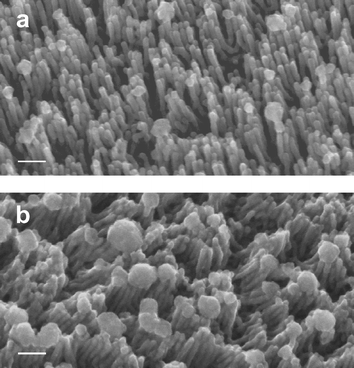 | ||
| Fig. 3 SEM images of (a) freestanding, electrodeposited nanowires following UV degradation of the PFS matrix and (b) freestanding wires following solvent dissolution of the PFS matrix in toluene. The PFS-PLA template was aligned using an electric field strength of 155 V µm–1. The scale bar represents 100 nm. | ||
PFS-PLA films annealed with an applied electric field of 80 V µm–1 also showed highly ordered arrays on the top surface (as in Fig. 2). Interestingly, following successful electrodeposition through these films and removal of the PFS phase with UV irradiation we found a disordered freestanding structure of branched nanowires (Fig. 4). This result shows that at a reduced electric field it is possible to obtain continuous channels through the film despite not forming a hexagonally ordered array of cylinders spanning the entire film thickness.
 | ||
| Fig. 4 SEM image of electrodeposited nanowires using a nanoporous PFS template prepared from a PFS-PLA thin film aligned using an electric field strength of 80 V µm–1. The scale bar represents 100 nm. | ||
This, on one hand, directly reflects the competition between the surface energy difference of the two blocks at both surfaces that results in a preferential alignment of the microphase morphology parallel to both surfaces and the electric field, causing them to stand up. These surface forces are clearly stronger at the more polar Au bottom surface compared to the top surface which was in contact with PDMS. On the other hand, these results also demonstrate that the electric field is able to overcome grain boundaries in the microphase morphology which are common in the bulk and in thin films with asymmetrical boundaries. Our results demonstrate the long-range order that can be induced in copolymer films by electric fields in a direct fashion.
In addition to the effect of the electric field strength on the degree of ordered alignment through the film, we also observed structural differences attributable to the alignment kinetics. Fig. 5 shows cross sectional SEM images of two films filled electrochemically after annealing under identical field strengths of 155 V µm–1 for (a) 14 h and (b) 35 h. The PFS matrix supports the nanowire structures in both cases. After 14 h the upper third of the film cross section shows ordered structures parallel to the electric field, while the lower portion of the film is disordered as in the image shown in Fig. 4. After 35 h annealing the aligned structures are clearly ordered through the full cross section. These results suggest that regions close to the upper surface are the first to fully align with the electric field.
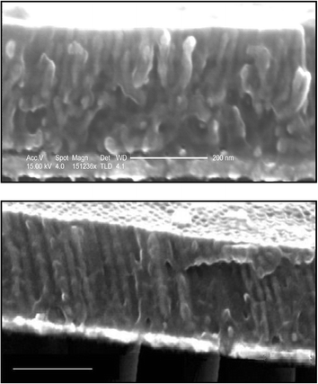 | ||
| Fig. 5 Cross sectional SEM images of electrodeposited nanowires in a nanoporous PFS template annealed for (a) 14 h (b) 35 h under a field of 155 V µm–1. The scale bars represent 200 nm. | ||
Conclusion
In conclusion, we have shown that a new cylinder forming block copolymer with sufficient dielectric contrast and a sacrificial block (PLA) that can be removed under mild conditions is useful as a template for the electrochemical growth of freestanding nanowire arrays. The method by which the template (PFS) is removed after nanowire deposition affects the clustering of the nanowire arrays. Furthermore, the electric field strength and duration play an important role in the degree of order in both the PFS templates and resulting nanowire arrays. Electric fields that are too low or that are not applied for long enough times lead to either nanopores that do not span the entire film thickness or a disorganized, branched nanoporous structure that is nonetheless amenable to nanowire deposition. Further development of this “soft-etch” technology will open the door to nanoscale templating of functional polymer systems such as conjugated polymers for photovoltaic applications.Experimental
Synthesis of poly(4-fluorostyrene)-b-poly(D,L-lactide) [PFS-PLA]
First, the PLA block was synthesized by the controlled, aluminium-catalyzed ring-opening polymerization of D,L-lactide using a mixture of benzyl alcohol and triethyl aluminium as the initiating system. The polymerization was carried out in toluene at 90 °C for 5 h and terminated with acidic water. The resulting hydroxy terminated polylactide was converted to the corresponding trithiocarbonate by reaction with the acid chloride of S-1-dodecyl-S′-(α,α′-dimethyl-α″-acetic acid) trithiocarbonate using an established procedure.24 The molecular weight of the resulting macromolecular chain transfer agent was determined to be 10 kg mol–1 by 1H NMR spectroscopy (assuming one trithiocarbonate moiety per chain), consistent with the targeted PLA molecular weight and conversion of lactide. The PDI of this material by size-exclusion chromatography (SEC) was determined to be 1.12. The controlled reversible addition fragmentation transfer (RAFT) polymerization25 of 4-fluorostyrene was carried out by first dissolving a 0.4 g portion of this functionalized PLA in 1.6 g of 4-fluorostyrene (purified by passage through an alumina column). The solution was degassed and then heated in a sealed flask to 120 °C for 6.3 h. Autoinitiation of the 4-fluorostyrene was the likely source of initiating free radicals. The resulting solid was dissolved in methylene chloride, precipitated in methanol, and the white powder was dried under reduced pressure at 75 °C. By SEC , a distinct shift to higher molecular weight was observed for the PFS-PLA product compared to the PLA starting material, and the PDI of PFS-PLA was 1.17. By 1H NMR spectroscopy, the overall molecular weight of PFS-PLA was 30 kg mol–1 corresponding to a PLA mass fraction of 0.33.Template preparation
Thin films of PFS-PLA (∼300 nm) were spin-cast from toluene solutions onto gold-coated silicon substrates. The upper-electrode was prepared from a 25 µm sheet of Kapton CR (Dupont) with a 50 nm thermally evaporated Au layer on the reverse side. In order to make conformal contact with the polymer layer, a thin layer (∼4.5 µm) of poly(dimethylsiloxane) (PDMS , Sylgard 184, Dow Corning) was spin-cast on the front side of the Kapton sheet from a 30 wt% solution in chloroform and cross-linked at 80 °C for 10 h. A potential difference between 2 and 4 kV was applied to the entire ensemble which was annealed at 140 °C in a N2 atmosphere for 14 or 35 h, and cooled to RT before removing the applied voltage. The calculated field inside the PFS-PLA film was 80 to 155 V µm–1. The films were subsequently immersed in 0.05 M NaOH solutions in water–methanol (60 : 40 by vol.) at room temperature for 6 h in order to remove the minority PLA component. An etching solution of bromine in methanol (80 : 1 wt bromine : methanol) was used to etch the underlying Au substrate layer and release the film following the PLA degradation. This allowed AFM imaging of the underside of the film.Electrochemical deposition
Nanowires were grown potentiostatically in a standard three-electrode setup using a CH Instruments potentiostat. Either pure Au substrates or Au substrates supporting the nanoporous templates on top were used as working electrodes, a platinum mesh acted as counter electrode and a silver/silver chloride (3 M KCl) electrode was used as the reference electrode. The electrolyte solution consisted of 0.4 M cupric sulfate and 3 M lactic acid in a methanol–water mixture (40 : 60 by volume). The presence of methanol is crucial in the electrolyte solution, since it ensures sufficient wetting of the pores by the solution. The pH was adjusted to pH 9 using sodium hydroxide.22 The deposition was performed at 55 °C at a constant potential of –0.4 V. Following deposition, the material was characterized with X-ray diffraction analysis using a Philips X'Pert PW3020 diffractometer with CuKα radiation (λ = 1.540598 Å). Films deposited on pure Au substrates gave evidence of a mixture of copper and copper oxide (Cu2O), with the majority phase being copper. To remove the PFS template after electrodeposition we used either a 15 min exposure to 172 nm UV radiation from a SUS-128 excimer radiation system (Ushio Europe B.V.) or simple dissolution in toluene.Imaging
Atomic force microscopy (AFM) and scanning electron microscopy (SEM ) were used to investigate the surface structure of the materials. AFM images were obtained using a Nanoscope IV (Digital Instruments 3100) in tapping mode with a silicon cantilever of resonant frequency 250–400 kHz. SEM imaging was performed on a FEI Philips XL30 sFEG at an accelerating voltage of 10 kV with no additional coating. Cross sectional images were obtained by immersing the entire sample in liquid nitrogen and fracturing the substrate.Acknowledgements
We thank Steve Scroggins for providing S-1-Dodecyl-S′-(α,α′-dimethyl-α″-acetic acid) trithiocarbonate and Dr Rajeswari Kasi for SAXS analysis of PFS-PLA. M. A. H. thanks the Leverhulme Trust for support under their Visiting Professorship program. S. L. and U. S. acknowledge financial support from the European network “Polyfilm” under RTN-6.References
- I. W. Hamley, The Physics of Block Copolymers, Oxford University Press, Oxford, 1998 Search PubMed.
- M. Li, C. A. Coenjarts and C. K. Ober, Adv. Polym. Sci., 2005, 190, 183 CAS.
- M. A. Hillmyer, Adv. Polym. Sci., 2005, 190, 137 CAS.
- M. Park, P. M. Chaikin, R. A. Register and D. H. Adamson, Appl. Phys. Lett., 2001, 79, 257 CrossRef CAS.
- M. J. Misner, H. Skaff, T. Emrick and T. P. Russell, Adv. Mater., 2003, 15, 221 CrossRef CAS.
- G. Liu and J. Ding, Adv. Mater., 1998, 10, 69 CrossRef CAS.
- C. Park, J. Yoon and E. L. Thomas, Polymer, 2003, 44, 6725 CrossRef CAS.
- U. Jeong, D. U. Ryu, D. H. Kho, J. K. Kim, J. T. Goldbach, D. H. Kim and T. P. Russell, Adv. Mater., 2004, 16, 533 CrossRef CAS.
- Y. Lin, A. Böker, J. He, J. Sill, H. Xiang, C. Abetz, X. Li, J. Wang, T. Emrick, S. Long, Q. Wang, A. Balazs and T. P. Russell, Nature, 2005, 434, 55 CrossRef CAS.
- S. H. Kim, M. J. Misner, T. Xu, M. Kimura and T. P. Russell, Adv. Mater., 2004, 16, 226 CrossRef CAS.
- Y. Xuan, J. Peng, L. Cui, H. Wang, B. Li and Y. Han, Macromolecules, 2004, 37, 7301 CrossRef CAS.
- G. Krausch and R. Magerle, Adv. Mater., 2002, 14, 1579 CrossRef CAS.
- J. Peng, Y. Xuan, H. Wang, Y. Yang, B. Li and Y. Han, J. Chem. Phys., 2004, 120, 11163 CrossRef CAS.
- S. O. Kim, H. H. Solak, M. P. Stoykovich, N. J. Ferrier, J. J. de Pablo and P. F. Nealey, Nature, 2003, 424, 411 CrossRef CAS.
- T. Xu, C. J. Hawker and T. P. Russell, Macromolecules, 2005, 38, 2802 CrossRef CAS.
- T. Thurn-Albrecht, R. Steiner, J. DeRouchey, C. M. Stafford, E. Huang, M. Bal, M. Tuominen, C. J. Hawker and T. P. Russell, Adv. Mater., 2000, 12, 787 CrossRef CAS.
- T. Thurn-Albrecht, J. Schotter, G. A. Kästle, N. Emley, T. Shibauchi, L. Krusin-Elbaum, K. Guarini, C. T. Black, M. T. Tuominen and T. P. Russell, Science, 2000, 290, 2126 CrossRef CAS.
- R. Olayo-Valles, M. S. Lund, C. Leighton and M. A. Hillmyer, J. Mater. Chem., 2004, 14, 2729 RSC.
- R. Olayo-Valles, S. Guo, M. Lund, C. Leighton and M. Hillmyer, Macromolecules, 2005, 38, 10101 CrossRef CAS.
- L. D. Landau, E. M. Lifshitz and L. P. Pitaevskii, Landau and Lifshitz Course of Theoretical Physics, Electrodynamics of Continuous Media, Pergamon Press, New York, 2nd edn, 1984, vol. 8, p. 44 Search PubMed.
- T. Xu, C. J. Hawker and T. P. Russell, Macromolecules, 2003, 36, 6178 CrossRef CAS.
- A. E. Rakhshani and J. Varghese, Thin Solid Films, 1988, 157, 87 CrossRef CAS; T. D. Golden, M. G. Shumsky, Y. Zhou, R. A. VanderWerf, R. A. Van Leeuwen and J. A. Switzer, Chem. Mater., 1996, 8, 2499 CrossRef CAS.
- Y. Liang, C. Zhen, D. Zou and D. Xu, J. Am. Chem. Soc., 2004, 126, 16338 CrossRef CAS.
- J. Rzayev and M. A. Hillmyer, J. Am. Chem. Soc., 2005, 127, 13373 CrossRef CAS.
- G. Moad, E. Rizzardo and S. H. Thang, Aust. J. Chem., 2005, 58, 379 CrossRef CAS.
Footnotes |
| † The HTML version of this article has been enhanced with colour images. |
| ‡ Present address: Institut für Makromolekulare Chemie, Albert-Ludwigs-Universität Freiberg, 79104 Freiberg, Germany. |
| § Permanent address: Department of Chemistry, University of Minnesota, Minneapolis, MN 55455-0431, USA. |
| This journal is © The Royal Society of Chemistry 2007 |