Ultrawide ZnO nanosheets
Jae-Hwan
Park
*,
Heon-Jin
Choi
,
Young-Jin
Choi
,
Seong-Hyung
Sohn
and
Jae-Gwan
Park
Materials Science and Technology Division, Korea Institute of Science and Technology, PO Box 131, Cheongryang, Seoul 130-650, Korea. E-mail: parkjh@kist.re.kr
First published on 27th November 2003
Abstract
Ultrawide ZnO nanosheets together with their formation mechanism have been reported. As the width and thickness of the sheets are in the range of 50–100 µm and 50–100 nm respectively, the width-to-thickness ratios of the sheets reach up to one thousand.
Bottom-up approaches to nanoelectronics using nanoscale building blocks such as quantum dots, nanowires, and nanotubes have received considerable attention to date.1–3 However, the feasibility of realizing highly integrated functional devices is still questionable due to the difficulties in the alignment and assembly of the building blocks. In this regard, the creation of new types of nanostructures of various sizes and shapes would be of interest. Here, we report on “seeable and touchable” ultrawide ZnO nanosheets which can be easily manipulated by conventional lithography and/or assembly techniques, while maintaining nano-sized features.
Our objective was to grow well-aligned 2D and 3D nanostructures of ZnO semiconducting oxide, which is one of the most promising materials for electronic and optoelectronic applications, by a carbothermal reduction process.4,5 Equal amounts of ZnO and graphite powders (99.9%, ∼325 mesh) were mixed and transferred to an alumina boat inside the processing tube. Above the alumina boat, Si substrates coated with 5–30 Å of Au were loaded. The nanostructures were fabricated on an Au-coated silicon substrate by heating a 1 ∶ 1 mixture of ZnO and graphite under a constant flow of gases for 5–120 min. The processing temperature varied from 800 °C to 950 °C and the amount of additional oxygen was controlled in the range of 1–20% with 20 sccm of Ar gas. By controlling the processing temperature and oxygen contents systematically, we could synthesize various 2D and 3D nanostructures including nanowires and nanosheets. The predominant structures under certain processing temperatures and oxygen contents can be categorized as shown in Fig. 1. We note here that the nanosheet structure is far different from the various well-known ZnO nanostructures.6–10
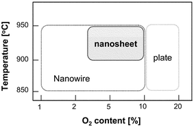 | ||
| Fig. 1 A summary of the predominant structures of ZnO under certain processing temperatures and oxygen contents. | ||
Fig. 2 shows scanning electron microscope images of ultrawide ZnO nanosheets obtained under a specified range of experimental conditions as illustrated in Fig. 1. As the width and thickness of the sheets are in the ranges of 50–100 µm and 50–100 nm respectively, the width-to-thickness ratio of the sheets reaches up to one thousand, i.e. the aspect ratio of writing paper. The length of the sheets reaches several mm. There have been a few reports on nanobelts and nanoribbons, whose widths were several hundred nm and the width-to-thickness ratios were in the range of 3–10.7,8 Thus, they have been categorized as 1D nanowires with different cross-sectional shapes. The ultrawide nanosheets in this work, however, could be categorized as 2D nanostructures due to their high width-to-thickness ratios.
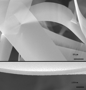 | ||
| Fig. 2 SEM images of the ultrawide nanosheets. The inset shows the edge of the sheet. | ||
We then examined the formation mechanism of such wide nanosheets by controlling the growth time.11Fig. 3a shows the sequential evolutionary stages of the nanosheets with the processing time. At first, 1D nanowires are grown. As the reaction time increases, dendritic sidebranch nanowires begin to grow along the basal nanowires, resulting in highly defined and aligned comb-like architectures. With further heat treatment, the sidebranches continue to grow and planar filling of the interspaces between the evenly spaced sidebranches proceeds, eventually resulting in an ultrawide nanosheet.
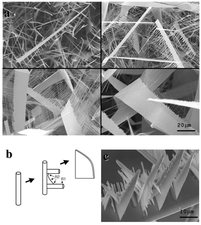 | ||
| Fig. 3 (a) SEM images showing the evolutionary stages of the nanosheets from the comb-like structure toward the sheet structure, which were obtained by controlling the growth time from a few seconds to several hours. (b) A schematic illustration showing the possible growth mechanism of the ultrawide nanosheets. (c) Hierarchical 3D arrays of nanosheets. | ||
It is noteworthy that the ultrawide nanosheets in this study are not formed in a continuous layer-by-layer fashion, but by a “1D branching and subsequent 2D interspace filling” process. We can summarize this process as illustrated in Fig. 3b. At first, nanowires are grown by the well-known vapor–liquid–solid (VLS) mechanism via an Au catalyst.4 As we could not detect any Au catalyst along the dendritic sidebranches from quantitative analysis, the comb-like sidebranching from the basal nanowire can not be attributed to the VLS mechanism. Dendritic crystals are fairly common in bulk crystals and usually result from the diffusion-limited and supersaturated vapor environment. In such an environment, the morphological instability can initiate, via a vapor–solid (VS) growth mechanism without catalyst, dendrites typically observed in fern-like ice crystals.12,13 Thus, the dendritic comb-like sidebranching in this work could be related to the diffusion-limited supersaturated environments. The intentional injection of O2 gas in our process seems to offer the excessive supersaturation level of reactant vapors. As the processing temperature and the oxygen content increase, the nanostructures evolve from 1D (nanowires) to 2D (sheets), and eventually, 3D (plates) structures as described earlier in Fig. 1a. From this result, we can also suspect that the dendritic sidebranching is related to the supersaturation of reactant vapors. The planar filling of the sidebranch interspaces can be attributed to the selective condensation of vapors on the concave corner sites between the branches (R2), where the chemical potential (i.e. equilibrium partial vapor pressure) is lower than the other convex (R1) or flat surface sites according to the Gibbs–Thomson relation. In summary, the growth of ultrawide nanosheets can be described with three sequential mechanisms: (i) basal nanowire formation (VLS process with catalyst), (ii) sidebranching (VS process by supersaturation), and (iii) planar filling (selective condensation). Fig. 3c shows the “sheets on a sheet” structure, i.e. hierarchical 3D arrays of nanosheets, with an extreme case of supersaturation and processing time. Upon a basal nanosheet, several sheets are aligned vertically. Furthermore, smaller sheets are initiated along the vertically aligned sheets: nanosheets are hierarchically arrayed and combined.
Fig. 4 shows transmission electron microscope (TEM) analysis for the nanowire, dendritic sidebranches, and interspaces evolving between the sidebranches. The nanowires are growing along the [0![[1 with combining macron]](https://www.rsc.org/images/entities/char_0031_0304.gif) 10] direction whereas dendritic sidebranches grow along the [0001] direction. The selected area electron diffraction (SAED) analysis confirms that the nanostructure is a single crystal of wurtzite structure. In Fig. 4(b), SAED patterns for every position, including S1 (sheet) and S2 (wire), were exactly identical as shown in the inset.
10] direction whereas dendritic sidebranches grow along the [0001] direction. The selected area electron diffraction (SAED) analysis confirms that the nanostructure is a single crystal of wurtzite structure. In Fig. 4(b), SAED patterns for every position, including S1 (sheet) and S2 (wire), were exactly identical as shown in the inset.
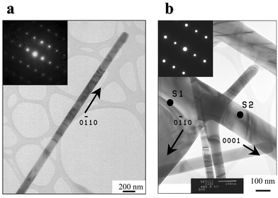 | ||
| Fig. 4 Transmission electron microscopy (TEM) analysis for (a) the nanowire and (b) dendritic sidebranches and interspaces evolving between the sidebranches. | ||
The width-to-thickness ratio of one thousand in this work is incomparably higher than those of nanoribbons or nanobelts. It means that the “1D branching and 2D filling” process presented here is a unique and efficient way to prepare ultrawide nanostructures. We believe that the growth process of the ultrawide ZnO nanosheets presented here could be applied to generate highly defined and hierarchical planar nanostructures of other material systems by controlling supersaturation levels of reactant vapors. We note that the ultrawide nanosheets and nanocombs are large enough to see with the human eye and to handle with TEM tweezers, while still maintaining nanosizes in their thickness directions.
As the ZnO nanosheets are large enough, they would be easy manipulable into specific architectures without arduous lithography on a nanometer scale. Due to their good crystallinity, semiconductivity, and high specific surface area, this kind of structure may find applications in sensors, optoelectronics, catalysts, and electrochemical nanodevices.
Notes and references
- P. Alivisatos, Pure Appl. Chem., 2000, 72, 3 Search PubMed.
- Y. Xia, P. Yang, Y. Sun, Y. Wu, B. Mayers, B. Gates, Y. Yin, F. Kim and H. Yan, Adv. Mater., 2003, 15, 353 CrossRef CAS.
- H. Dai, Surf. Sci., 2002, 500, 218 CrossRef CAS.
- M. H. Huang, Y. Wu, H. Feick, N. Tran, E. Weber and P. Yang, Adv. Mater., 2001, 13, 113 CrossRef CAS.
- Y. Chen, X. Cui, K. Zhang, D. Pan, S. Zhang, B. Wang and J. G. Hou, Chem. Phys. Lett., 2003, 369, 16 CrossRef CAS.
- J. G. Wen, Chem. Phys. Lett., 2003, 372, 717 CrossRef CAS.
- Z. W. Pan, Z. R. Dai and Z. L. Wang, Science, 2001, 291, 1947 CrossRef CAS.
- J. Liu, J. Cai, Y.-C. Son, Q. Gao, S. L. Suib and M. Aindow, J. Phys. Chem. B, 2002, 106, 9761 CrossRef CAS.
- H. Q. Yan, J. Am. Chem. Soc., 2003, 125, 4728 CrossRef CAS.
- Z. R. Dai, Z. W. Pan and Z. L. Wang, Adv. Funct. Mater., 2003, 13, 9 CrossRef CAS.
- To observe the evolutionary stages from nanowires to nanosheets, we tried to control the growth time of the synthesis. It is, however, impossible to limit the reaction time down to a few seconds at elevated temperatures higher than 800 °C. Thus, we controlled the injection time of oxygen gas. As the oxygen gas is crucial to forming the comb-like and sheet-like structures from the basal nanowires, it is possible to adjust the reaction time practically by controlling the flow valve of O2 from a few seconds to several hours at elevated temperatures.
- W. W. Mullins and R. F. Sekerka, J. Appl. Phys., 1964, 35, 444.
- D. T. J. Hurle, Handbook of Crystal Growth Vol.1b, North-Holland, Amsterdam, 1993 Search PubMed.
| This journal is © The Royal Society of Chemistry 2004 |