Engineered films for display technologies
William A.
MacDonald
DuPont Teijin Films, PO Box 2002 Wilton, Middlesbrough, UK TS90 8JF. E-mail: bill.a.macdonald@gbr.dupont.com
First published on 21st November 2003
Abstract
Flexible displays and flexible electronics is an area generating considerable interest at present. This article will discuss the requirements of a base substrate for flexible displays and contrast the plastic films that are being developed for this application. The review will cover how the surfaces and properties of the films are being engineered to make them suitable for laying down barrier coatings and for laying down thin film transistor arrays. The barrier technologies that are being developed and the issues facing the development of a “flexible glass” will be discussed.
 Bill MacDonald | Bill MacDonald studied chemistry at The University of St Andrews and joined the ICI Plastic Division in 1980. He was initially involved in research into advance materials, primarily liquid crystal polymers, and moved into the Polyester Films Business in the early 1990s. The Films Business was sold to DuPont and Bill MacDonald is currently a Business Research Associate in DuPont Teijin Films, a 50 ∶ 50 Joint Venture between DuPont and Teijin. He has coauthored 37 papers including several book chapters and has filed 9 patents. DuPont Teijin Films is the world's premier producer of PET and PEN polyester films. They specialise in film products and related services for application areas including Safety and Protection, Security, Imaging, Printing and Recording media, Advanced photo systems, Electronics Packaging and Industrial Applications. The company has reported sales of $1.4 billion and employs about 4,000 people in all regions of the world. Earlier this year DuPont Teijin Films UK Ltd. received a Queen's Award for Enterprise in the Innovation category, for its development of Melinex® Core 1. This material was developed largely at the company's global research and development centre based at Wilton in the NE of England. www.dupontteijinfilms.com |
Introduction
There is currently considerable interest in flexible displays1,2 and many electronic based companies currently are actively researching flexible displays based on primarily liquid crystal displays (LCD),3–5 organic light emitting diodes (OLEDs)6–8 and electrophoretic displays.9 An example of a flexible OLED display is shown in Fig. 1.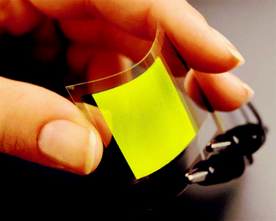 | ||
| Fig. 1 Photograph of a flexible OLED display (courtesy of DuPont Displays). | ||
Flexible displays offer substantial rewards in terms of being able to develop displays that are thinner, lighter, robust, conformable and can be rolled away when not required. In addition plastic based substrates coupled with the recent developments in solution deposition and ink jet printing for laying down OLED materials10 and active matrix thin film transistor (TFTs) arrays11 open up the possibility of cost effective processing in high volumes using roll to roll processing.12 To replace glass however, a plastic substrate needs to be able to offer the properties of glass i.e. clarity, dimensional stability, thermal stability, barrier, solvent resistance, low coefficient of thermal expansion (CLTE) coupled with a smooth surface. No plastic film offers all these properties so any plastic based substrate will almost certainly be a multilayer composite structure.1,2 This review will discuss and contrast the leading candidates for plastic based flexible substrates and discuss the technologies being developed to meet the demanding barrier targets. It should be noted that this is a fast evolving field and some of the results discussed in the literature may not represent what the flexible substrate suppliers would (or will in the future) present as their preferred tailored candidates. The author in this review has tried to present a comparison based on his knowledge of the available substrates at this time.
Polymer substrates
This review will focus only on plastic films that have been given serious consideration as flexible substrates for flexible electronics. The main candidates are shown in Fig. 2 which lists the substrates in terms of increasing glass transition (Tg).13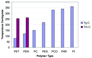 | ||
| Fig. 2 Comparison of a range of plastic substrates by glass transition. | ||
The polymers can be further categorised into films that are semi-crystalline, amorphous, but thermoplastic and amorphous, but solvent cast. The group of thermoplastic semi-crystalline polymers includes polyethylene terephthalate (PET)
e.g. DuPont Teijin Films Melinex®![[thin space (1/6-em)]](https://www.rsc.org/images/entities/char_2009.gif) 14 and polyethylene naphthalate (PEN)
e.g. DuPont Teijin Films Teonex®.14 PEN with a Tg of ∼120 °C, is in the upper temperature range for the semi-crystalline thermoplastic polymers that can still be melt processed. Polymers with Tg's higher than 140 °C tend generally to have melting points that are too high to allow the polymers to be melt processed without significant degradation. The next category are polymers that are thermoplastic, but non-crystalline and these range from polycarbonate (PC)
e.g. Teijins PURE-ACE®15 and GE's Lexan®16 with a Tg of ∼150 °C to polyethersulfone (PES)
e.g. Sumitomo Bakelite's Sumilite®17 with a Tg of ∼220 °C. Although thermoplastic these polymers may also be solvent cast to give high optical clarity. The third category are high Tg materials that cannot be melt processed and include aromatic fluorene containing polyarylates (PAR)
e.g. Ferranias Arylite®,18 polycyclic olefin (PCO-also known as polynorbornene)
e.g. Promerus's Appear®19 and polyimide (PI)
e.g. DuPont's Kapton®.20
14 and polyethylene naphthalate (PEN)
e.g. DuPont Teijin Films Teonex®.14 PEN with a Tg of ∼120 °C, is in the upper temperature range for the semi-crystalline thermoplastic polymers that can still be melt processed. Polymers with Tg's higher than 140 °C tend generally to have melting points that are too high to allow the polymers to be melt processed without significant degradation. The next category are polymers that are thermoplastic, but non-crystalline and these range from polycarbonate (PC)
e.g. Teijins PURE-ACE®15 and GE's Lexan®16 with a Tg of ∼150 °C to polyethersulfone (PES)
e.g. Sumitomo Bakelite's Sumilite®17 with a Tg of ∼220 °C. Although thermoplastic these polymers may also be solvent cast to give high optical clarity. The third category are high Tg materials that cannot be melt processed and include aromatic fluorene containing polyarylates (PAR)
e.g. Ferranias Arylite®,18 polycyclic olefin (PCO-also known as polynorbornene)
e.g. Promerus's Appear®19 and polyimide (PI)
e.g. DuPont's Kapton®.20
This review will focus primarily on the crystalline biaxially oriented films which have different properties compared to amorphous films and for simplicity these two basic categories will be used when comparing and contrasting the properties of the film types.
Optical properties
Clarity of the film is important for bottom emissive displays and a total light transmission (TLT) of >85% over 400–800 nm coupled with a haze of less than 0.7% are typical of what is required. All the base films in Table 1 except for polyimide which is yellow meet this criteria with polycarbonate in particular having excellent optical properties.| Base polymer | PET14 | PEN14 | PC15,16 | PES17 | PAR18 | PCO19 | PI20 |
|---|---|---|---|---|---|---|---|
| a CLTE. b Not available. c N.B. The information in this table is taken from different datasheets and should only be taken as illustrative. | |||||||
| CTE (−55 to 85 °C) ppm/°C | 15a | 13a | 60–70 | 54 | 53 | 74 | 30–60 |
| %Transmission (400–700 nm) | >85 | 0.85 | >90 | 90 | 90 | 91.6 | Yellow |
| Water absorption (%) | 0.14 | 0.14 | 0.4 | 1.4 | 0.4 | 0.03 | 1.8 |
| Young's modulus/GPa | 5.3 | 6.1 | 1.7 | 2.2 | 2.9 | 1.9 | 2.5 |
| Tensile strength/MPa | 225 | 275 | NAb | 83 | 100 | 50 | 231 |
For top emissive displays clarity in the base substrate is not essential and this opens up the possibility of building display devices on non transparent substrates such as stainless steel or polyimide which is yellow. However top emissive displays will still need an optically clear barrier film as an encapsulant.
Biaxially oriented films such as polyethylene terephthalate and polyethylene naphthalate are birefringent. The dependence on light of known polarisation in LC displays means that birefringent films, which would change the polarisation state, are unlikely to be used as substrates. Films based on amorphous polymer are not birefringent and are more suitable for LC displays. Birefringence is not an issue with OLED displays.
Thermal properties
Thermal and dimensional stability are critical, in enabling a film to withstand the high temperatures of deposition of the barrier and indium tin oxide coatings; to ensure precision registration of the different layers in the final device; and for the multilayer device to be able to withstand thermal cycling. Plastic films undergo a variable and undesirable change in dimensions at the ‘Tg’, due to both molecular relaxation events associated with the increased mobility of the polymer chains and also ‘shrinkage’ or ‘expansion’ associated with the relaxation of residual strain within the oriented parts of the film structure. With biaxially oriented polyesters this is a consequence of the film manufacturing conditions. However, it is important to consider what are the key property requirements when choosing materials for device manufacture — ‘Tg’ is an obvious characteristic to focus on initially. Polymers undergo a change in physical and mechanical properties at the glass transition ‘Tg’. However for OLED manufacture it is not the change in mechanical properties that is of prime importance, but rather the control of the dimensional reproducibility as the film is cycled in temperature. This is manifested in two ways. Firstly, the shrinkage a film undergoes when heated and then cooled to the starting temperature. Low levels of shrinkage are desired to make accurate alignments on the substrates after each thermal processing step. Secondly, the natural expansion of the film as temperature is cycled as measured by the coefficient of linear thermal expansion (CLTE). A low CLTE typically <20 ppm/°C is desirable to match the thermal expansion of the base film to the layers which are subsequently deposited.3 A mismatch in thermal expansion means that the deposited layers become strained and cracked under thermal cycling.
Polyethylene terephthalate and polyethylene naphthalate films with Tg's of 78 and 120 °C respectively would at first sight be considered to have too low a Tg to impart the thermal and dimensional stability necessary to support OLED manufacture. However, the dimensional stability of polyethylene terephthalate and polyethylene naphthalate films can be enhanced by a heat stabilisation process,13,21,22 in which the internal strain in the film is relaxed by exposure to high temperature whilst under minimum line tension. The majority of polymer films, when heated to temperatures above the nominal Tg, show some tendency to shrink or expand along selected axes. Shrinkage at a given temperature is measured by placing the sample in a heated oven for a given period of time. The percentage shrinkage is calculated as the % change of dimension of the film in a given direction or molecular axis before and after the heating process. Heat-stabilised polyethylene naphthalate film exhibits minimal shrinkage in the order of <0.1% and typically <0.05% when exposed to temperatures of up to 180 °C for 5 minutes. In addition, once heat stabilised, the Tg effects described above are essentially negated and polyethylene naphthalate film remains a dimensionally reproducible substrate up to 200 °C i.e. within the performance requirements of a flexible substrate for an OLED display. Polyethylene terephthalate film exhibits minimal shrinkage up to 150 °C. How the dimensions change with temperature and time is clearly illustrated by results from thermal mechanical analysis carried out using a thermomechanical analyser (TMA-7, Perkin Elmer). These data compare heat stabilised 125 micron polyethylene naphthalate film to non-heat stabilised 125 micron polyethylene naphthalate film (Fig. 3)13,22 and heat stabilised polyethylene naphthalate film to heat stabilised polyethylene terephthalate film (Fig. 4).
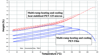 | ||
| Fig. 3 Thermal mechanical analysis of 125 micron polyethylene naphthalate (PEN) and heat stabilised polyethylene naphthalate (PEN) films. | ||
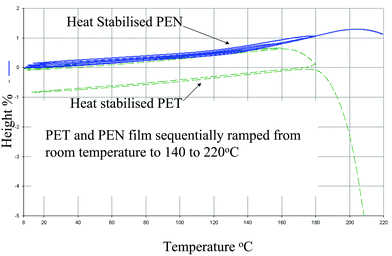 | ||
| Fig. 4 Thermal mechanical analysis of heat stabilised polyethylene terephthalate (PET) and polyethylene naphthalate films. | ||
In the evaluation, the films have been heated and subsequently cooled between 8 °C and 140 °C, 160 °C, 180 °C and 220 °C respectively and any permanent change in dimensions on cooling back to room temperature before the next heating cycle are recorded in the y-axis. This is illustrated in Fig. 3 where heat stabilised polyethylene naphthalate film follows reproducibly the same expansion and contraction path as the sample is heated through the Tg and to higher temperatures and then cooled. Under the same conditions, non stabilised polyethylene naphthalate film remains dimensionally stable up to 120 °C, but shrinks above this temperature. Heat stabilised polyethylene terephthalate film follows the same expansion and contraction path up to 150 °C (Fig. 4).
The rates of expansion against temperature vary and are known to be dependent on factors such as draw ratio, heat setting temperatures and subsequent heat treatment or thermal mechanical history. The coefficient of linear thermal expansion (CLTE) values13 (Table 2) are generally lower than for most equivalent polyethylene terephthalate based films (by ∼25%) and the higher glass/rubber transition, Tg, for polyethylene naphthalate film would mean that relaxation events (related to increased molecular mobility), would also therefore occur at relatively higher temperatures.
|
CLTE
PPM −50 to 0 °C |
CLTE
PPM 0–50 °C |
CLTE
PPM 50–100 °C |
CLTE
PPM 100–150 °C |
|
|---|---|---|---|---|
|
Machine
direction |
13 | 16 | 18 | 25 |
|
Transverse
direction |
8 | 11 | 18 | 29 |
Once shrinkage, or additional expansion effects, (principally due to release of residual strain effects within the oriented parts of the structure) have been removed by the heat stabilisation process outlined above, the changes in the CLTE value with temperature are essentially predictable. The differential measured along the two principal axes, machine direction (MD) and transverse direction (TD), reflects the degree of orientation within each molecular axis within the plane of the polyethylene naphthalate film; i.e. the lower the CLTE value the higher the degree of orientation. The CLTE value for unoriented isotropic polyethylene naphthalate by comparison is measured at ∼35 ppm/°C. In common with the majority of polymer systems, there will be an increase in relative CLTE values above the Tg, and for a heat stabilised polyethylene naphthalate film. This will predominantly depend upon the natural or intrinsic thermal expansion of the film. Non-stabilised film on the other hand will undergo additional relaxation due to the removal of unrelaxed stress and strain effects which can result in permanent deformation.
Taking the CLTE and shrinkage data together, heat stabilised polyethylene terephthalate and polyethylene naphthalate films are therefore dimensionally predictable substrates below the temperature ranges at which they have been heat stabilised. It is the ability to firstly limit and secondly to predict changes in dimension with temperature that are exploited in the OLED manufacturing process.
The amorphous family of polymers exhibit very low shrinkages when cycled to temperatures below their respective Tg's and therefore the higher the Tg the higher the operating window although there are limits on this (see below). However, amorphous polymers typically have CLTE of the order of 50 ppm/°C (Table 1).
Recent research has shown that the shrinkage values of both amorphous and semicrystalline films can be pushed further by annealing the films at elevated temperatures for extended periods of time. Polyimide, polyarylate and polycyclic olefin films exhibited shrinkages of <10 ppm h−1 when annealed at 300 °C for 10–100 h.23,24 Polyethersulfone exhibited a similar shrinkage when annealed at 180 °C for a similar period of time.3 Polyethylene naphthalate shrinkages of 25 ppm during thin film transistor backplane processing, after an annealing process have recently been reported.25
In addition to dimensional stability another important factor to be considered is the upper processing temperature (Tmax) that a film can be used at. Although as outlined above the Tg does not define Tmax with the semi-crystalline polymers, it largely does with the amorphous polymers. However again the picture is not quite as simple as that as the films based on amorphous polymers may be hardcoated to give solvent resistance (see next section) and the Tmax is then defined by the thermal stability of the hardcoat. This can bring Tmax down to 220 °C for some of the solvent cast amorphous polymers.
Moisture and solvent resistance
A wide range of solvents and chemicals can potentially be used when laying down the various layers in the display depending on the processing steps involved. Amorphous polymers in general have poor solvent resistance compared to semi-crystalline polymers. This deficiency is overcome by the application of a hard coat to the amorphous resins which significantly improves the solvent and chemical resistance to solvents such as NMP, IPA, acetone, methanol, THF, ethyl acetate, 98% sulfuric acid, glacial acetic acid, 30% hydrogen peroxide and saturated bases such as sodium hydroxide.24An area that has not been discussed in the literature is the effect of water absorption on dimensional stability where the levels of water absorbed can be of an order that will have a considerably detrimental effect on dimensional stability. This will become increasingly important as processing moves towards roll to roll. Polyethylene terephthalate and polyethylene naphthalate films have an inherent advantage over the amorphous polymers films being both semi-crystalline and biaxially oriented polymers and typically will absorb approximately 1400 ppm of moisture at equilibrium (the exact figure depending upon temperature and relative humidity). Polyethersulfone and polyimide films are particularly problematic and will absorb over 1% moisture at equilibrium.17,20 Polycyclic olefin film is an exception to the above and has a very low moisture absorption level of 300 ppm.19
Although pre-annealing the substrate can greatly reduce shrinkage and careful process design can reduce the effects of swelling due to solvents and water, it is very likely that alignment equipment will require special adaptations.
Mechanical properties
Production of glass based displays currently involves moving batches of glass between the different processing stages. The mechanical difference, in particular stiffness, between rigid glass and flexible substrates will likely require very different methods of processing polyethylene terephthalate and polyethylene naphthalate films are inherently stiffer than amorphous films with their Young's Modulus being typically three times higher — an artefact of being semi-crystalline and biaxially oriented (Table 1). This stiffness may prove to be an advantage in the current batch based display manufacturing process.Surface quality
The surface smoothness and cleanliness of the flexible substrates are both essential to ensure the integrity of subsequent layers such as barrier and conductive coatings (see the section on Barriers). In the case of polyethylene terephthalate and polyethylene naphthalate films improvements in surface quality can be achieved through control of recipe and film process. This is demonstrated in Figs. 5, 6 and 7 which highlights the substantial reduction of surface defect peaks with two different grades of polyethylene naphthalate film.13,22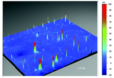 | ||
| Fig. 5 Surface smoothness of industrial grade polyethylene naphthalate (PEN) film. | ||
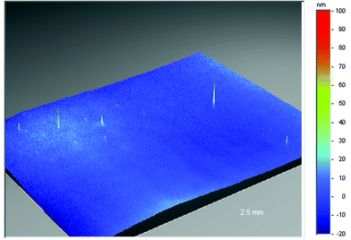 | ||
| Fig. 6 Surface smoothness of untreated Teonex® Q65 (polyethylene naphthalate (PEN) film). | ||
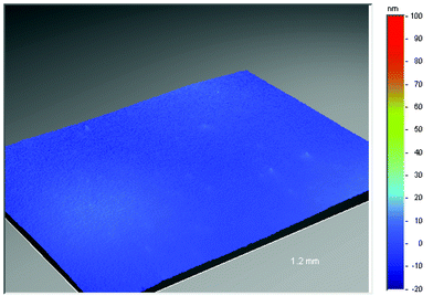 | ||
| Fig. 7 Surface smoothness of surface tailored Teonex® Q65 (polyethylene naphthalate (PEN) film). | ||
A 2.5 millimeter square area of industrial grade polyethylene naphthalate (Fig. 5), as measured using conventional non-contacting, white-light, phase-shifting interferometry techniques (the instrument used was a Wyko NT3300 surface profiler), contains over ten peaks greater than 100 nanometers in height and numerous peaks over 50 nanometers. A comparison of this to optical grade polyethylene naphthalate (Teonex® Q65) (Fig. 6), where only five peaks greater than 50 nanometers exist throughout the same measured area, indicates how the surface quality can be controlled by recipe and process optimisation alone. The surface defects which remain in the Teonex® Q65 however are still detrimental to the performance of thin overlying layers. To remove these entirely requires the application of a coating layer, typically comprised of a scratch resistant material. This acts to smooth over all the underlying polyethylene naphthalate surface defects and additionally helps to prevent surface scratches on handling. The coated film surface is now tailored for the deposition of subsequent layers. Fig. 7 depicts the surface topography of a surface tailored Teonex® Q65 over a 1.2 millimeter square area and demonstrates that all the surface defects are removed. Polyarylate and polycyclic olefin films are also surface coated to both improve surface quality and also give solvent resistance.24
Barriers
One of the key properties of any substrate that replaces glass will be to offer glass-like barrier properties. OLED materials in particular are 10,000 times more sensitive than LCD's to moisture and oxygen. This is because the OLED and component layers are of the order of 50 nm and any defect that protrudes from the surface by 100 nm or more is likely to cause a defect. In addition the OLED materials are themselves chemically unstable in the presence of air and moisture and degrade thereby creating black spots and ruining a display.The plastic substrates that are under consideration as flexible substrates typically have barriers of the order 1–10 g m−2 day−1 for water vapour transmission rate and of ca. 1–10 mL m−2 day−1 for oxygen. OLED displays will require water vapour transmission rates of <10−6 g m−2 day−1 and oxygen transmission rates of <10−5 mL m−2 day−1. No polymer meets this extremely demanding requirement.
A major issue in the development of barrier substrates is how to measure barriers at this level. At present there is no standard method for measuring water vapour permeabilities below 5 × 10⁻³ g m−2 day−1 and 5 × 10⁻³ mL m−2 day−1 for oxygen. A calcium degradation test has been developed by researchers in Philips.26–28 This involves depositing a thin calcium layer on glass in an oxygen and water free environment which is then encapsulated with a thin film barrier within the same vacuum system. The calcium layer which is initially a metallic mirror degrades to an increasingly transparent layer of calcium salt. Automated image analysis of the photos yields the distribution of optical transmission of the calcium layer. Optical modelling of the transmission of calcium–calcium salt stacks enables determination of the distribution of the calcium oxide thickness in the cell. The latter can then be related to the amount of absorbed water as a function of time, yielding the effective permeation rate of the encapsulant. Water vapour transmission rates down to 10−6 g m−2 day−1 have been reported.
Barrier coatings on films have been extensively researched for a number of years29–37 because of the necessity to prolong the shelf-life of packaged food products by reducing water and oxygen ingress and metal and dielectric layers are now routinely coated on polymers for this purpose with great success. However the permeability specification for OLED applications is several orders of magnitude lower than that for food packaging27,38 and for optical applications it is of course not possible to use opaque metal films.
In principle, a perfect layer of silica only a few nanometres thick should reduce the diffusion of water and oxygen to acceptable levels (just as the 2–3 nanometres native oxide layer on silicon wafers protects the wafer surface from further oxidation). The problem in practice is that thin film coatings can have defects that provide easy paths for water and oxygen molecules to penetrate.31 Also, surface defects on the polymer substrates cause pinholes in the final coating and lead to catastrophic failure of barrier properties. However, even clean, pinhole-free coatings are not perfect. In the particular case of vacuum-deposited thin film barrier coatings, this is due to the tendency of such films to show columnar growth and to exhibit densities less than the bulk material.35 Water and oxygen molecules can then diffuse through the nano-spacings between columns.39 On the relatively rough surfaces of normally processed polymer sheet this effect is enhanced. Heating substrates to elevated temperatures can help reduce columnar growth but this option is not open with all polymer substrates.
Thin film diffusion barrier encapsulants and substrates based on vacuum deposited organic–inorganic multi layers offer a promising route to transparent packaging for OLED displays.39–43 Several organisations are currently developing optically transparent multilayer barrier coatings for flexible substrates. The approach being used by Vitex Systems typifies the technology being used. Their barrier coating, called Barix®,44 is comprised of alternating layers of polymer and ceramic film applied in vacuum. The total thickness of the coating is about 3 microns. In this technology a liquid acrylate is applied under vacuum to the surface of the film and this is then UV cured. This coating covers any imperfections and provides an atomically smooth surface. Next, a ceramic film, only about 500 angstroms thick, is deposited on top of the polymer layer. Because the surface is so smooth, the ceramic film has very few defects and is therefore an almost perfect moisture barrier. This process is repeated creating a stack of multiple polymer and ceramic layers in which each ceramic film is a near-perfect moisture barrier. This combination of ceramic and polymer layers, with a total thickness of about 3 microns, creates a moisture barrier whose water permeability has been measured in the range of 10−6 g m−2 day−1 and OLED displays on barrier coated of polyethylene terephthalate with preliminary operating lifetimes of >200 h have been reported. An electron micrograph of a barrier coating is shown in Fig. 8 and a simplified schematic of a passive matrix OLED display is shown in Fig. 9.
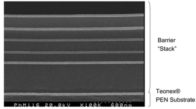 | ||
| Fig. 8 Electron micrograph of barrier structure (SEM courtesy of Vitex Systems). | ||
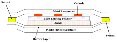 | ||
| Fig. 9 Schematic of a passive matrix OLED display. | ||
Bottom emission displays are currently encapsulated in metal cans. The move towards higher specification displays will require active matrix addressing and this will likely require silicon based thin film transistors on the substrate. These may partially block light thereby reducing the display efficiency and putting a limit on resolution. A transparent barrier film opens up the possibility of designing the display so that the light exits the top of the display, significantly boosting the efficiency and enabling much higher resolution.
The requirements for OLED displays are particularly demanding. In the course of developing barrier technologies for this application it is likely that films with improved barrier performance for example water permeability in the range of 10−3 g m−2 day−1 will be developed and these will find application in less demanding devices such as electronic paper.
Mechanical properties of the composite structure
As outlined above the final engineered substrate will be a multilayer structure. Issues such as adhesion at the interface between the different layers under thermal cycling and environmental testing, curl, the wetting characteristics, ability to withstand flex testing etc. must be critical to determining their robustness in use. To date there has been very little published work in this area and there is an important need to both define test protocols and determine how the structures behave on testing. Published work to date has focused on the behaviour of transparent conductive coatings on flexible substrates on flexing,45,46 but this is outside the scope of this review.Fabrication
Discussion on the move from patterned indium tin oxide based passive matrix displays towards active matrix displays and whether amorphous silicon thin film transistors (TFTs) or poly-silicon TFT's or organic based TFT's are the most suitable devices for active matrix is beyond the scope of this article. Simply stated however, the technology direction will be towards active matrix addressing as this offers benefits with regard to high image quality and is almost certainly essential for larger displays. There are two possible methods of fabrication for flexible displays:3(i) standard poly-silicon TFT fabrication on glass substrates and transfer of the array to a polymer substrate
(ii) direct fabrication on the polymer substrate itself.
The first approach has been demonstrated by several research groups47,48 and offers the benefits that the TFT array can be manufactured on existing production lines once the transfer process has been established. The cost will always be higher than for a glass based display because of the wasted glass substrate and the additional transfer process. However low temperature flexible substrates can subsequently be used.
Direct fabrication is a more attractive option but there are significant issues with regards to active matrix technology and manufacturing equipment. There are three basic approaches and although again detailed discussion is beyond the scope of this article these approaches can be used to highlight the pros and cons of the various options.
(i) to develop novel low temperature processes (<200 °C) for building silicon based TFT's that can be carried out on the lower temperature performance substrates (semi-crystalline and amorphous melt processable films). This option has the benefit of using lower cost substrates but may require new processing technology for silicon based TFT's to achieve the desired mobilities.
(ii) to adapt existing silicon processes to reasonably low temperature (250–300 °C) for use on higher temperature films (amorphous solvent cast films). This route exploits existing silicon processing technology but will likely require new substrate development as none of the existing amorphous cast films offer the ideal property mix (CLTE <20 ppm/°C, good colour and ability to withstand a processing temperature of 300 °C).
(iii) to exploit organic based TFTs with processing temperatures <200 °C depending on the coating process. The ink jet printing11 of organic based TFT's is a genuine game changing technology which pushes processing temperatures down below 120 °C — at these processing temperatures polyethylene terephthalate starts to become viable as a substrate and it has a considerable cost advantage over the other film options.
All three approaches are currently being explored and again detailed discussion is beyond the scope of this article. However as a generalisation there is a technology trend towards lower processing temperatures which favours the lower temperature and lower cost film substrates.
Concluding remarks
No particular display technology will serve all applications and several technologies will coexist. This means that all the substrates discussed in this article will likely find use and that the choice of a substrate for a particular application will depend on the operating requirements of that particular technology. This general area of structural materials underpinning functional materials opens up new avenues of material research that can build on the fundamental science that has been developed in the structural polymers and composites area. It is also likely that the material developments made to underpin the display area will find spin-offs into other technology areas. The fabrication technology is also evolving and the requirements for the substrate will change as advances are made.Engineered substrates for display application are still at a development stage and there are many technical issues still to be resolved, but the attractiveness of flexible displays is such that flexible displays will be commercialised — the question is not if but when.
Acknowledgements
The author would like to acknowledge contributions from Karl Rakos and Robert Eveson of DuPont Teijin Films, Phil Willcocks of ICI and Prof. Frank Placido of the University of Paisley.References
- P. J. Slikkerveer, Inf. Disp., 2003, 3, 20–24 Search PubMed.
- P. J. Slikkerveer, Conference Proceedings from 22nd International Display Research Conference, 2002, 273–276.
- N. D. Young, M. J. Trainor, S-Y Yoon, D. J. McCulloch, R. W. Wilks, A. Pearson, S. Godfrey, P. W. Green, S. Roosendaal and E. Hallworth, Mater. Res. Soc. Symp. Proc., 2003, 769, paper H2.1.
- S. H. Won, C. B. Lee, H. C. Nam, J. Jang, J. K. Chung, M. Hong, B. S. Kim, Y. U. Lee, S. H. Yang, J. M. Huh and K. Chung, Society For Information Display, Digest of Technical Papers, 2003, 992–995 Search PubMed.
- Y. H. Kim, S. K. Park, J. I. Han, D. G. Moon and W. K. Kim, Society For Information Display, Digest of Technical Papers, 2003, 996–999 Search PubMed.
- K. Heeks and S. Hough, Inf. Disp., 2003, 4&5, 14–19 Search PubMed.
- J. G. Innocenzo, R. A. Wessel, M. O'Regan and M Sellars, Society For Information Display, Digest of Technical Papers, 2003, 1329–1335 Search PubMed.
- A. B. Chwang, M. A. Rothman, S. Y. Mao, R. H. Hewitt, M. S. Weaver, J. A. Silvernail, K. Rajan, M. Hack, J. J. Brown, X. Chu, L. Moro, T. Krajewski and N Rutherford, Society For Information Display, Digest of Technical Papers, 2003, 868–871 Search PubMed.
- Y. Chen, J. Au, P. Kazlas, A. Ritenour, H. Gates and M. McCreary, Nature, 2003, 423, 136 CrossRef CAS.
- C. MacPherson, M. Anzlowar, J. Innocenzo, D. Kolosov, W. Lehr, M. O'Regan, P. Sant, M. Stainer, S. Sysavat and S. Venkatesh, Society For Information Display, Digest of Technical Papers, 2003, 1191–1193 Search PubMed.
- H Sirringhaus, S. E. Burns, C Kuhn, K. Jacobs, J. D. MacKenzie, M. Etchells, K Chalmers, P. Devine, N. Murton, N. Stone, D Wilson, P. Cain, T. Brown, A. C. Arais, J. Mills and R. H. Friend, Society For Information Display, Digest of Technical Papers, 2003, 1084–1087 Search PubMed.
- R. van den Berg, Displays Europe, 2001,(Autumn), 15–19 Search PubMed.
- B. A. MacDonald, K. Rollins, R. Eveson, K. Rakos, B. A. Rustin and M. Handa, Mater. Res. Soc. Symp. Proc., 2003, 769, paper H9.3.
- Melinex™, Teonex™, DuPont Teijin Films Luxembourg S.A., P.O. Box 1681, L-1016 Luxembourg.
- PURE-ACE™, Teijin Chemicals Ltd., 1-2-2 Uchisaiwai-cho, Chiyoda-ku, Tokyo, Japan.
- Lexan™, GE Plastics, One Plastics Ave., Pittsfield, MA 01201, USA.
- Sumilite™, Sumitomo Bakelite Co. Ltd., Ten-Nouzu Parkside Blgd., 5-8,2-Chome, Higashi-Shinagawa, Shinagawa-Ku, Tokyo, 140-0002, Japan.
- Arylite™, Ferrania S.p.A.,Centro Direzionale, Via Rivoltana, 2/d, Edificio A ,I 20090 Segrate (MI), Italy.
- Appear™, Promerus LLC, 9921 Brecksville Road, Brecksville, Ohio 44141, USA.
- Kapton™, DuPont High Performance Films, P.O. Box 89, Route 23 South and DuPont Road, Circleville, OH 43113, USA.
- W. A. MacDonald, J. M. Mace and N. P. Polack, 45th Annual Technical Conference Proceedings of the Society of Vacuum Coaters, 2002, 482.
- W A MacDonald, K Rollins, R Eveson, R A Rustin and M Handa, Society For Information Display, Digest of Technical Papers, 2003, 264–267 Search PubMed.
- S. Angiolini, M. Avidano, R. Bracco, C. Barlocco, R Bracco, J. J. Bacskay, J.-H. Lipian, P. S. Neal, L. F. Rhodes, R. A. Shick, X-M. Zhao and G Freeman, Society For Information Display, Digest of Technical Papers, 2000, 1–4 Search PubMed.
- S. Angiolini, M. Avidano, R. Bracco, C. Barlocco, N. G. Young, M Trainor and X.-M Zhao, Society For Information Display, Digest of Technical Papers, 2003, 1325 Search PubMed.
- K. R. Sarma, C. Chanley, S. Dodd, J. Roush, J. Schmidt, G. Srdanov, M. Stevenson, R. Wessel, J. Innocenzo, G. Yu, M. O'Regan, W. A. Macdonald, R. Eveson, K. Long, H. Gleskova, S. Wagner and J. C. Sturm, Proceedings from SPIE Aerosense, Techologies and Systems for Defense and Security, April 22–25, 2003 (to be published).
- G. Nisato, P. C. P. Bouten, P. J. Slikkerveer, W. D. Bennet, G. L. Graff, N. Rutherford and L. Wiese, Proceedings Asia, Display/IDW 2001, 1435.
- G. Nisato, P. C. P. Bouten, P. J. Slikkerveer, W. D. Bennett, G. L. Graff, N. Rutherford and L. Weise, SID J.,, 2001,(Nov.) Search PubMed.
- G. Nisato, M Kuilder, P. Bouten, L Moro, O. Philips and N. Rutherford, Society For Information Display, Digest of Technical Papers, 2003, 550–553 Search PubMed.
- W. Prins and J. J. Hermans, J. Phys. Chem., 1959, 63, 716 CrossRef CAS.
- E. H. H. Jamieson and A. H. Windle, J. Mater. Sci., 1983, 18, 64–80 CAS.
- G. Rossi and M. Nulman, J. Appl. Phys., 1993, 74, 5471 CrossRef.
- R. W. Philips, T. M. Markantes and C. LeGallee, 36th Annual Technical Conference Proceedings of the Society of Vacuum Coaters, 1993, 293.
- S. Amberg-Schwab, M. Hoffmann, H. Bader and M. Gessler, J. Sol-Gel Sci. Technol., 1998, 1(2), 141 Search PubMed.
- U. Moosheimer and H.-C. Langowski, 42nd Annual Technical Conference Proceedings of the Society of Vacuum Coaters, 1999, 408.
- B. M. Henry, A. G. Erlat, C. R. M. Grovenor, C. S. Deng, G. A. D. Briggs, T. Miyamoto, N. Noguchi, T. Niijima and Y. Tsukahara, 44th Annual Technical Conference Proceedings of the Society of Vacuum Coaters, 2001, 469.
- A. W. Smith, N. Copeland, D. Gerrard and D. Nicholas, 45th Annual Technical Conference Proceedings of the Society of Vacuum Coaters, 2002, 525.
- B. M. Henry A. G. Erlat C. R. M. Grovenor G. A. D. Briggs Y. Tsukahara, 45th Annual Technical Conference Proceedings of the Society of Vacuum Coaters, 2002, 503.
- R. D. Maixner, 45th Annual Technical Conference Proceedings of the Society of Vacuum Coaters, 2002, 461.
- H.-C. Langowski, A. Melzer and D. Schubert, 45th Annual Technical Conference Proceedings of the Society of Vacuum Coaters, 2002, 471.
- J. D. Affinato, M. E. Gross, C. A. Coronado, G. L. Graff, E. N. Greenwell and P. M. Martin, Thin Solid Films, 1996, 290–291, 63–67 CrossRef.
- I. C. Bright, US Patent 20020022156A1, 2000.
- G. L. Graff, M. E. Gross, M. K. Shi, M. G. Hall, P. M. Martin and E. S. Mast, WO 01/81649 A1, 2001.
- G. L. Graff, M. E. Gross, M. K. Shi, M. G. Hall, P. M. Martin and E. S. Mast, WO 01/82389 A1, 2001.
- Barix®, Vitex Systems Inc., 3047 Orchard parkway, san Jose, CA 95134.
- S. Gorkhali, D. R. Cairns and G. P. Crawford, Society For Information Display, Digest of Technical Papers, 2003, 1332–1335 Search PubMed.
- P. C. T. Bouten, 22nd International Display Research Conference Conference Proceedings, 2002, 313–316.
- A. Asano and T. Kinoshita, Society For Information Display, Digest of Technical Papers, 2002, 37 Search PubMed.
- C. Berge, T. A. Wagner, W. Brendle, C Craff-Castillo, M. B. Schubert and J. H. Werner, Mater. Res. Soc. Symp. Proc., 2003, 769, paper H2.7.1.
| This journal is © The Royal Society of Chemistry 2004 |