
 Open Access Article
 This Open Access Article is licensed under a
 Creative Commons Attribution 3.0 Unported Licence
Improved stability and electronic homogeneity in perovskite solar cells via a nanoengineered buried oxide interlayer†
W. Hashini K.
Perera
 a,
Tony J.
Woodgate
a,
Dong Kuk
Kim
b,
Rachel C.
Kilbride
c,
Mateus G.
Masteghin
a,
Christopher T. G.
Smith
a,
Steven J.
Hinder
d,
Sebastian
Wood
b,
K. D. G. Imalka
Jayawardena
*a and
S. Ravi P.
Silva
*a
a,
Tony J.
Woodgate
a,
Dong Kuk
Kim
b,
Rachel C.
Kilbride
c,
Mateus G.
Masteghin
a,
Christopher T. G.
Smith
a,
Steven J.
Hinder
d,
Sebastian
Wood
b,
K. D. G. Imalka
Jayawardena
*a and
S. Ravi P.
Silva
*a
aAdvanced Technology Institute, School of Computer Science and Electronic Engineering, University of Surrey, Guildford, Surrey GU2 7XH, UK. E-mail: s.silva@surrey.ac.uk; i.jayawardena@surrey.ac.uk
bElectromagnetic and Electrochemical Technologies Department, National Physical Laboratory, Teddington, Middlesex, TW11 0LW, UK
cDepartment of Chemistry, University of Sheffield, Sheffield S3 7HF, UK
dThe Surface Analysis Laboratory, Faculty of Engineering and Physical Sciences, University of Surrey, Guildford, Surrey GU2 7XH, UK
First published on 20th February 2025
Abstract
Self-assembled monolayers (SAMs) are a popular choice for achieving high-efficiency perovskite solar cells (PSCs). However, the incomplete wetting of the perovskite on (4-(3,6-dimethyl-9H-carbazol-9-yl)butyl)phosphonic acid (Me-4PACz) SAMs in PSCs has proven to be a challenge. Recently, the use of surface modifiers such as alumina nanoparticles and poly(9,9-bis(3′-(N,N-dimethyl)-N-ethylammonium-propyl-2,7-fluorene)-alt-2,7-(9,9-dioctylfluorene))dibromide (PFN–Br) has been demonstrated to eliminate this bottleneck. However, the influence of these surface modifiers on device stability has not been reported. Here, we studied the influence of alumina nanoparticles and PFN–Br on Me-4PACz device stability when stressed under ISOS-D-2I and ISOS-D-2 conditions (at 65 °C). The use of alumina nanoparticles leads to efficient scavenging of iodine, improved bulk electrical and surface electronic homogeneity in fresh films, which is preserved even when the films are degraded, and the formation of 2D perovskites, which act as a barrier against moisture induced degradation. In comparison, perovskites based on PFN–Br show a distinct lack of similar characteristics for fresh and degraded samples. This allows the realisation of alumina modified Me-4PACz based PSCs with a tenfold improved T80 lifetime of 1530 h under ISOS-D-2 conditions compared to the PFN–Br based device stack. Our study uncovers a new approach towards enhancing PSC stability, which could potentially be applied under more strenuous ISOS test conditions to further improve device stability.
Broader contextSelf-assembled monolayers (SAMs) have emerged as contact modifiers that enable high efficiency perovskite solar cells (PSCs) to be realised. Within the vast family of SAM molecules, hydrophobic molecules have been a key driver towards realising high efficiencies. However, improving the device yield on such hydrophobic molecules requires surface modifiers such as alumina nanoparticles and conjugated polyelectrolytes such as poly(9,9-bis(3′-(N,N-dimethyl)-N-ethylammoinium-propyl-2,7-fluorene)-alt-2,7-(9,9-dioctylfluorene))dibromide (PFN–Br). Despite the adoption of these surface modifiers, there is a lack of studies focusing on the influence of molecular modifiers on the nanoscale electrical and electronic properties of the perovskite and device stability. In this work, we show that PSCs utilising alumina nanoparticles as a surface modifier on SAMs have higher device stability in comparison to devices with PFN–Br. We further show that alumina nanoparticles, compared to PFN–Br, result in multiple beneficial effects including the homogenisation of surface electronic properties and bulk electrical conduction, both of which do not significantly vary when degraded under heat and ambient conditions. Alumina is further shown to contribute to scavenging of iodine that can form during the degradation of perovskites, leading to improved device stability. Our work provides a new pathway for improving both the performance homogeneity and stability of PSCs. |
Introduction
Perovskite solar cells (PSCs) have shown impressive growth in power conversion efficiencies (PCE) over the last decade, since their first implementation in 2009.1 However, the lack of long-term device stability remains a key challenge that must be overcome to ensure their commercial potential.2 For well-established material technologies like silicon, qualification standards such as those described by the International Electrotechnical Commission (IEC) (e.g., IEC 61215-1 (ref. 3)) are implemented. However, due to the fundamental differences in the material and device properties of PSCs in comparison to silicon, protocols developed for organic photovoltaics (PVs) at the 2010 International Summit on Organic PV Stability (ISOS), Roskilde, Denmark,4 have been adopted, where stress test conditions for PSCs are now defined through either individual or multiple stressors applied to the device. For PSCs, this involves stressors such as light, heat (typically 65 °C or 85 °C), moisture and oxygen, which lead to device degradation through reaction pathways (1)–(4) (ref. 5 and 6) outlined below for a simple perovskite composition:| CH(N2H4)PbI3 ↔ CH(N2H4)I + PbI2 | (1) |
| CH(N2H4)I → CH(N2H3) + HI | (2) |
| PbI2 → Pb0 + I2 | (3) |
| CH(N2H3) → HCN + NH3 | (4) |
From the noted reaction pathways, the generation of molecular iodine (I2) as outlined in reaction (3) is a major factor inducing degradation processes in PSCs,7 particularly through electrochemical pathways. Once formed, I2, due to its highly volatile nature, can penetrate easily through the bulk of the perovskite, triggering chain reactions, which further degrade the perovskite.7,8 I2 is also known to drive halide segregation in mixed halide (I and Br) wide bandgap perovskites9–11 and oxidation and degradation of lead-tin mixed perovskites,12,13 with implications for high efficiency device architectures. Developing I2 trapping strategies to suppress I2 induced reactions is therefore crucial for achieving long-term stability in PSCs.
With a view to improving stability against I2 generated within PSCs, we screened for scavengers that can be incorporated under low temperature processing for PSCs. We specifically focused on I2 scavengers that are used in the nuclear industry, where I2 formed from the long-lived 129I and short-lived 131I is of particular concern due to its impact on the environment and human health.14 Among these, gamma-alumina (γ-Al2O3) is a well-known iodine scavenger in the nuclear industry and in environmental remediation, due to its high reactivity with I2.14 As reported by Miller et al., the adsorption of I2 onto surface hydroxyl (–OH) sites of γ-Al2O3 (henceforth referred to as Al2O3) proceeds via a highly energetically favourable pathway, leading to the formation of hydroxyl surface complexes.15
The use of Al2O3 in PSCs was first reported by Lee et al., where Al2O3 nanoparticles (NPs) were used as an insulating scaffold, resulting in a PCE of 10.9%.16 Guarnera et al. modified this architecture, incorporating an additional Al2O3 NP buffer layer in between the perovskite and the hole transporting layer (HTL) in an n–i–p device stack.17 This was shown to prevent the metal ion migration into the perovskite, thereby improving device stability. Subsequently, Al2O3 NPs were used to achieve dense perovskite absorbers on hydrophobic organic HTLs such as P3HT, PTAA and poly-TPD.18,19
PSCs based on self-assembled monolayers (SAMs) have also benefitted from the use of Al2O3 NPs, particularly devices based on the hydrophobic, methyl substituted carbazole based SAM, (4-(3,6-dimethyl-9H-carbazol-9-yl)butyl)phosphonic acid (Me-4PACz).20–22 Me-4PACz has been shown to enable fast hole extraction,23 which has led to its use in record efficiency perovskite/Si tandem cells since 2019,24 and also in the record perovskite/CIGS tandem device.25 However, the poor wettability of the perovskite on the Me-4PACz surface has also resulted in reproducibility challenges.20,26,27 Previously, we have addressed this challenge by modifying the Me-4PACz surface using Al2O3 NPs, which results in wettability improvement as well as enhanced recombination lifetimes, translating into efficiencies approaching 20%,20 an approach that is now widely reported in the literature.21
Here, we report a T80 lifetime of 1530 h for PSCs incorporating Al2O3 NPs when stressed under ISOS-D-2 conditions (65 °C and 35% relative humidity or RH), which is a more than 10 fold improvement compared to poly(9,9-bis(3′-(N,N-dimethyl)-N-ethylammonium-propyl-2,7-fluorene)-alt-2,7-(9,9-dioctylfluorene))dibromide (PFN–Br) based PSCs. This corresponds to a PCE of 13.1% at ∼1520 h for a champion cell with Al2O3 NPs, which demonstrated a starting PCE of 16.4% (note: for stability testing, Cu was used in place of Ag for the cathode contact as used for champion cells). We attribute this improved stability to multiple (beneficial) effects associated with the incorporation of Al2O3 NPs. Using optical spectroscopy, we demonstrate the effectiveness of Al2O3 NPs as an I2 scavenger, which in turn leads to lower I2 release from perovskite absorbers when thermally stressed. We further demonstrate that the surface potential of perovskites formed on Al2O3 NPs is more homogenised as compared to perovskites on PFN–Br, indicative of improved compositional homogeneity of the film, which reflects electrical homogeneity within the perovskite bulk. Our work provides new insights into an important, but hidden role played by Al2O3 NPs in PSCs as a nanoengineered interlayer that templates the structure above it.
Results and discussion
Iodine scavenging efficacy of Al2O3 NPs vs. PFN–Br
To demonstrate the enhanced iodine scavenging effect of Al2O3 NPs over PFN–Br, we periodically evaluated the change in the intensity of the ∼500 nm optical absorption feature of I2 (ref. 28 and 29) in I2/toluene solutions exposed to PFN–Br and Al2O3 NP powders. Over a duration of 5.5 h, a continuous reduction in the intensity of this absorbance peak was observed for I2/toluene exposed to Al2O3 NPs, while there was no noticeable change in I2/toluene exposed to PFN–Br (Fig. 1a–c and S1, ESI†). This is in agreement with the reported work on I2 scavenging by Al2O3 NPs.14 Further, the lack of any noticeable change in the absorbance intensity for I2 following the addition of PFN–Br indicates that it is unlikely to play a stabilising role of the perovskite absorber against I2 induced degradation.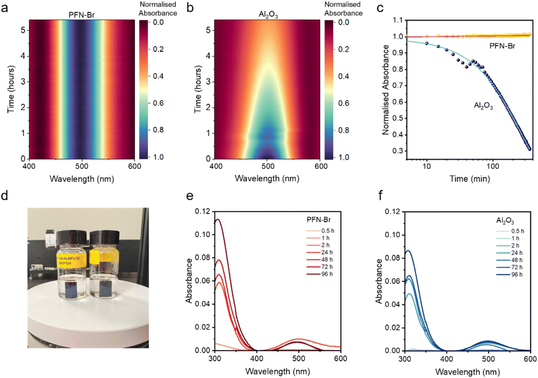 | ||
| Fig. 1 Study of the changes in I2 concentration in toluene with time. Heat maps showing the change in the I2 absorption peak intensity at 500 nm for toluene containing: (a) PFN–Br powder and (b) Al2O3 powder. (c) Temporal variation of I2 absorbance peak intensity for PFN–Br and Al2O3 normalised to the peak intensity at t = 0. The feature observed in (b) within the period of 40–60 min is attributed to changes in the lab environment, which is observed to affect the background of the spectrum. (d) Perovskite films deposited on PFN–Br and Al2O3 immersed in toluene to monitor the liberation of I2. UV-vis absorbance spectra of I2 liberated from the perovskite films deposited on (e) PFN–Br and (f) Al2O3. Curves corresponding to 0.5 h and 1 h are not visible in the figures due to the very weak absorbance signals at these time intervals resulting from very low generation of I2. | ||
We next studied the evolution of I2 from perovskite films formed on Me-4PACz modified with PFN–Br and Al2O3 NPs as the films are degraded. For this, Cs0.05FA0.79MA0.16Pb(I0.83Br0.17)3 films deposited on glass/Me-4PACz/(PFN–Br or Al2O3 NPs) were immersed in toluene and thermally degraded at a temperature of 65 °C in the dark, under ambient conditions, at a RH of ∼35% (Fig. 1d) to mimic the stress conditions used for ISOS-D-2 stability testing of devices discussed later. While the absence of the barrier layers as well as the C60, BCP and Cu layers in the films immersed in toluene can influence the degradation rate, the use of toluene as an I2 absorbing medium allows a relatively simple method to assess the iodine generation and escape for the above films. UV-vis optical absorption spectra of toluene were recorded periodically for 96 h to observe changes in the concentration of I2 generated as described by eqn (3) during the degradation of the perovskite absorber. For perovskite films on Me-4PACz/PFN–Br and Me-4PACz/Al2O3 NPs, the evolution of I2 was evaluated based on the I2 absorbance peaks at ∼310 nm in place of the peak at 500 nm, as the former peak shows a clear differentiation of I2 concentration over the period of study for these samples as compared to the 500 nm absorbance peak. We observed a higher intensity for the I2 absorbance peaks for perovskite films on Me-4PACz/PFN–Br (Fig. 1e and S2, ESI†) compared to perovskites on Me-4PACz/Al2O3 NPs (Fig. 1f), indicating that the I2 released during thermal degradation of the perovskite is scavenged by the NPs. Based on the absorbance measurements, it is evident that Al2O3 NPs can contribute towards improving device stability due to their ability to scavenge the iodine generated within the perovskite by moisture uptake. We note that Al2O3 NPs also provide additional benefits including homogenising the electrical characteristics of the bulk and the surface electronic properties, which contributes to an improved stability (discussed later).
Effect of the Me-4PACz surface modifier on device stability
Based on the observed efficacy of scavenging of I2 by Al2O3 NPs, its impact on device performance and stability was examined. For stability tests, a device architecture of glass/ITO/Me-4PACz/(Al2O3 or PFN–Br)/perovskite/C60/BCP/Cu as shown in Fig. 2a and g was used for comparing the performance of different perovskites. Fig. 2b shows the current density–voltage (J–V) curves of Cs0.05FA0.79MA0.16Pb(I0.83Br0.17)3 (bandgap ≈ 1.63 eV) on Me-4PACz, where similar to our previous work,20 devices with Al2O3 NPs show a higher PCE of 20.3% compared to a PCE of 15.8% for PFN–Br. The lower performance driven by losses for all device performance parameters for PFN–Br is attributed to higher recombination losses as well as reduced work function with PFN–Br treatment.20 We further utilised the Al2O3 NP modification strategy on a 1.55 eV Cs0.05FA0.85MA0.10PbI3 perovskite, which resulted in a champion PCE of 23.1%, while devices based on PFN–Br showed a champion PCE of 14.2%. The statistical distribution of the device performance parameters and the external quantum efficiency spectrum for the above are shown in ESI Fig. S3 and S4,† respectively. | ||
| Fig. 2 ISOS-D-2 and ISOS-D-2I stability testing of devices. (a) Device architecture of the PSCs used in this study (left) and a photograph of a device (right). (b) J–V curves of the champion devices fabricated on Me-4PACz modified with PFN–Br and Al2O3 for a 1.63 eV bandgap absorber. The device characteristics for a 1.55 eV perovskite absorber on Me-4PACz modified with Al2O3 and PFN–Br are also shown. Stability testing of devices modified with PFN–Br and Al2O3 under (c) ISOS-D-2I (n = 10) and (d) ISOS-D-2 (n = 8) conditions. Photographs of degraded devices are shown on the right. J–V curves in reverse scan direction of champion devices based on (e) PFN–Br under ISOS-D-2I conditions, (f) Al2O3 under ISOS-D-2I conditions, (g) PFN–Br under ISOS-D-2 conditions, and (h) Al2O3 under ISOS-D-2 conditions. | ||
For stability testing under ISOS-D-2 and ISOS-D-2I, devices were encapsulated with a moisture barrier layer consisting of poly(p-xylylene) sandwiched between two layers of diamond-like carbon, which we have previously reported as a moisture barrier coating for space applications and have undergone testing for space qualification.30 Under accelerated conditions of temperature and humidity (60 °C and 85% RH), this coating has excellent barrier properties with a low water permeation rate of approximately 4 × 10⁻³ g per m2 per day. This is significantly lower compared to the water uptake observed with single-layer alumina coatings.31 Further details of the moisture barrier coatings are reported in our previous work.30 The performance characteristics of the devices used for stability testing with Cu as the metal cathode are given in ESI Fig. S5.† Cu is typically preferred over Ag for stability testing due to the ion migration induced degradation of the latter.32 However, the use of Cu as the metal cathode also results in lower device performance,33 which explains the lower starting PCE observed for these devices. Further, for stability testing under ISOS-D-2 and ISOS-D-2I, the 1.63 eV perovskite absorber was chosen over the 1.55 eV absorber. This is due to the faster degradation of the latter absorber as a result of the thiocyanate additive as previously reported by us.12 Furthermore, while early studies suggested a correlation between higher device stability and higher device efficiency,34 recent research has shown that the highest-performing devices are not necessarily the most stable.35
For ISOS-D-2 stability testing, devices were placed in ambient air at a temperature of 65 °C and ∼35% RH. As shown in Fig. 2c, devices modified with PFN–Br show severe degradation, with >67% of their average initial PCE being lost over a test period of ∼2100 h. We estimated the average T80 lifetime of PFN–Br modified devices to be ∼160 h, while the T80 lifetime of the champion device was ∼139 h (ESI Fig. S6†). In comparison, devices based on Al2O3 NPs degraded over ∼2100 h showed superior stability, retaining >68% of their initial average PCE with an average T80 lifetime of 1350 h, while the champion device demonstrated a T80 value of ∼1530 h. These values correspond to an improvement in T80 lifetimes of over 8-fold (for average PCE) and over 10-fold (for champion PCE) compared to PFN–Br. To evaluate the impact of a perfect encapsulation, we assessed the degradation of similar devices fabricated in the same batch under ISOS-D-2I (dark, N2, and 65 °C) conditions. The variations in average and champion PCEs for these devices are given in Fig. 2d and ESI Fig. S6,† respectively. Considering the champion device PCE, a T80 lifetime of ∼750 h is estimated for the PFN–Br based PSC, while the device with Al2O3 NPs maintains more than 80% of its starting PCE following degradation for over ∼2100 h. While both device types maintain their PCEs following an initial degradation, it is evident that PFN–Br devices are less stable than devices with Al2O3 NPs, even when well encapsulated, which we attribute to a combination of I2 induced degradation and changes in the bulk electrical and surface electronic properties. Fig. 2e–h depict the J–V curves of the champion devices in reverse scan direction acquired during the aging period under both testing conditions (forward direction scans are given in ESI Fig. S7†). Under ISOS-D-2 testing, the severe degradation of PSCs with PFN–Br is dominated by losses in the device short circuit current density (JSC), open circuit voltage (VOC) and fill factor (FF) (ESI Fig. S8†). In comparison, performance parameters for PSCs with Al2O3 NPs demonstrate less severe degradation over the same testing period. Less degradation of device performance parameters is also observed under ISOS-D-2I testing for both PFN–Br and Al2O3 NP based devices (ESI Fig. S9†).
Chemical composition of degraded films
Subsequent to the degradation of devices, we characterised the perovskite absorber from degraded devices for chemical, structural and electronic changes to identify the reasons for improved stability of PSCs with Al2O3 NPs. To probe the perovskite absorber, the C60/BCP/Cu/moisture barrier coating stack was removed as shown in Fig. 3a for devices tested under ISOS-D-2 and ISOS-D-2I conditions (see the Experimental section for additional details). Following the peeling-off process, the samples were washed with chlorobenzene as reported by Yang et al.,36 to remove any residual C60 on the surface.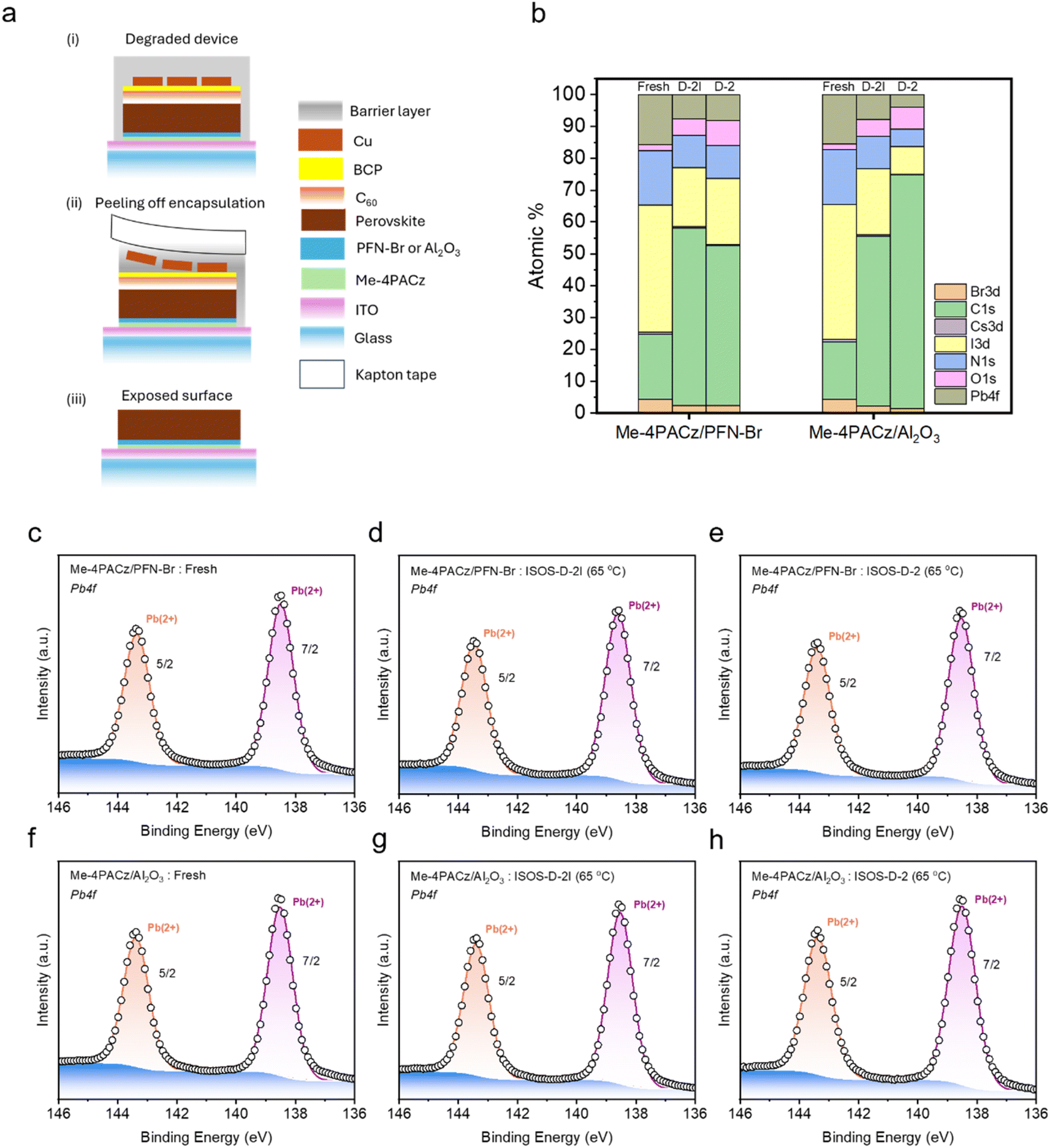 | ||
| Fig. 3 Study of the surface compositions of perovskites on PFN–Br and Al2O3. (a) Schematic showing the peeling off of the C60/BCP/Cu/moisture barrier layer from the degraded devices. (b) Surface composition analysis of fresh and degraded perovskite films on PFN–Br and Al2O3. Pb 4f XPS spectra of (c) fresh perovskite on PFN–Br, (d) perovskite on PFN–Br degraded under ISOS-D-2 conditions, (e) perovskite on PFN–Br degraded under ISOS-D-2I conditions, (f) fresh perovskite on Al2O3, (g) perovskite on Al2O3 degraded under ISOS-D-2 conditions, and (h) perovskite on Al2O3 degraded under ISOS-D-2I conditions. | ||
X-ray photoelectron spectroscopy (XPS) measurements were conducted on fresh and degraded (ISOS-D-2I and ISOS-D-2) perovskite films on PFN–Br and Al2O3 NPs (Fig. 3b–h and S10–S14, ESI†). We initially assessed changes in the elemental composition of the perovskite surface for fresh and degraded samples. The atomic percentages (atomic %) of elements are presented in Fig. 3b, showing contributions from Pb (from the B site of the perovskite), I and Br (from the X site of the perovskite), and Cs, C, N, and O. The O atomic % reflects exposure to ambient conditions and N atomic % is influenced by N2 from the glove box environment, ambient air, and organic cations, while the C atomic % is influenced by adventitious carbon and the organic cations in the perovskite. We eliminate the presence of C60 due to the absence of a peak at a binding energy (BE) of 290 eV (ESI Fig. S14†) corresponding to the π–π* shake-up peak.37 For perovskites on Al2O3 NPs, the Pb atomic % was estimated to be 15.4 at%, 7.7 at% and 3.9 at% for fresh, ISOS-D-2I and ISOS-D-2 degraded samples, respectively. This indicates that, within the probed depth of the samples (∼5 nm),38 thermal effects in an inert environment (ISOS-D-2I) lead to a decrease in Pb atomic %, with a further decrease being observed when the samples are degraded under ambient (ISOS-D-2) conditions. This decrease in Pb atomic % is attributed to the carbon enrichment at the surface. We note that, although the samples are encapsulated during degradation studies, some level of moisture penetration (∼0.08%) still occurs. While this can induce structural changes within the perovskite due to the limited solubility of lead salts in water, heating at 65 °C is expected to further impact the microstructure of the samples.
We analysed the Pb 4f and I 3d signals in detail to determine whether metallic Pb (Pb0) and I2 are formed in both fresh and degraded samples, as the formation of Pb0 and I2 signifies the degradation of the perovskite (eqn (3)). For both PFN–Br/perovskite and Al2O3 NP/perovskite, we observed a single Pb 4f7/2 peak at a BE of ∼138.5 eV, which corresponds to lead halides,39 while a peak corresponding to Pb0 (a BE of ∼136.2 eV)40 was not observed irrespective of whether the samples are fresh or degraded (Fig. 3c–h). In the I 3d spectra of PFN–Br and Al2O3 NP based samples, we observed a single peak at 619.4 eV, which corresponds to iodides,41 while no I2 peaks (expected to appear at 620 eV (ref. 42)) were detected irrespective of whether the samples are fresh or degraded (ESI Fig. S12†).
We studied the surface of the moisture barrier layer for the presence of any trapped I2 in the degraded samples (ESI Fig. S15†). For PSCs incorporating PFN–Br, we observed the presence of both iodides and I2 when the samples are degraded under ISOS-D-2 and ISOS-D-2I. For PSCs with Al2O3 NPs, an I2 signal was only visible when degraded under ISOS-D-2 conditions, while an I2 signal cannot be clearly identified when the samples are degraded under ISOS-D-2I conditions.
Based on eqn (3), it is evident that the generation of I2 proceeds simultaneously with the formation of Pb0. Since no distinct I2 signal is detected in either the fresh or degraded samples, it is likely that I2 formation occurs at levels below the detection limits of the XPS for both surface modifiers. This is probably due to the low moisture permeability provided by the barrier layers used for device encapsulation. Taking into consideration the I2 scavenging ability of Al2O3 NPs, it is also reasonable to expect that samples with this surface modifier will have lower I2 generation compared to samples with PFN–Br.
Electronic homogeneity at the surface
The influence of the modifiers on the surface electronic homogeneity of fresh and degraded samples was studied using scanning Kelvin probe force microscopy (KPFM, Fig. 4). KPFM offers nanoscale resolution mapping of surface potential and is able to resolve variations in chemical composition and homogeneity across the perovskite film, which have been associated with increased ionic motion and reduced operational stability.43,44 Surface potential is measured as the contact potential difference (CPD) with respect to the work function of the metallic probe. In this experimental configuration, a higher (more positive) CPD value corresponds to the sample having a smaller (shallower) work function (assuming a constant tip-work function). Whilst quantitative work function measurements are possible, the trends can be more precisely compared from the CPD data. Here, we observe clear differences in the distribution of surface potentials and the mean CPD values (ESI Fig. S16†). The corresponding topographic maps, representative scanning electron micrographs and grain size analyses are given in ESI Fig. S17–S19,† respectively. The histograms of CPD values for each pixel in the maps show a broad CPD distribution for fresh perovskite films on PFN–Br (Fig. 4a), which becomes narrower for degraded samples, with the narrowest distribution being observed for ISOS-D-2 samples. In comparison, a much narrower CPD distribution is observed for absorbers on Al2O3 NPs for both fresh and degraded films (Fig. 4b), while the change in CPD upon degradation is also significantly lower compared to films on PFN–Br. The width of the CPD distribution is indicative of the homogeneity of the material in terms of both chemical composition and the distribution of near-surface trap states. This suggests that the film incorporating Al2O3 NPs is more homogeneous. Inhomogeneous films with unpassivated surface trap states and grain boundaries have been shown to be more susceptible to degradation.43 As a result, the CPD distribution for such a sample will narrow as degradation progresses.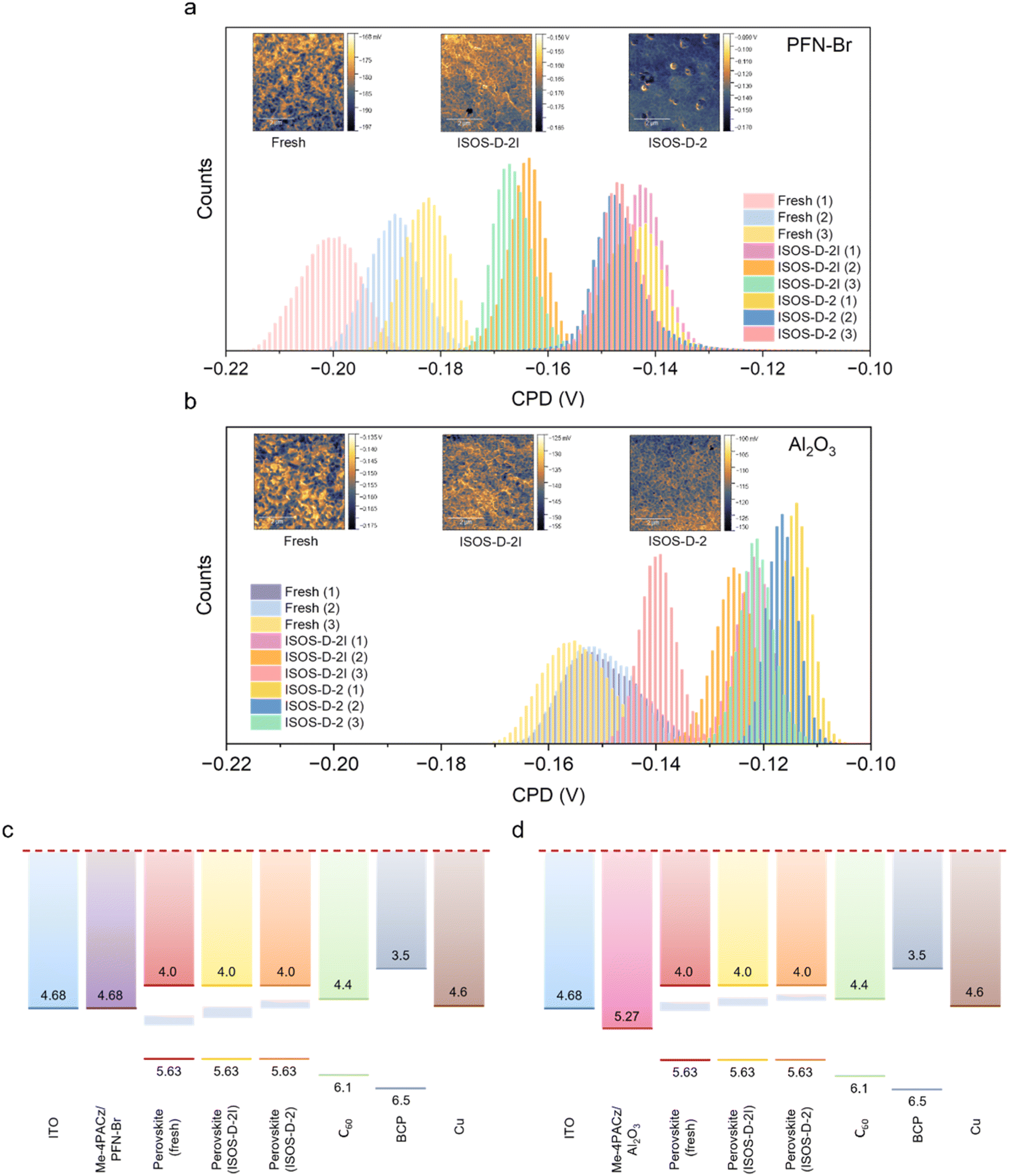 | ||
| Fig. 4 Electronic homogeneity of perovskites on PFN–Br and Al2O3. CPD distribution of fresh perovskite films and films degraded under ISOS-D-2 and ISOS-D-2I conditions, deposited on (a) PFN–Br and (b) Al2O3. CPD mappings of the samples are shown in the insets. Representative band diagrams for the devices studied in this work. The trends for the shift of the Fermi levels of the fresh and degraded perovskite absorbers on (c) PFN–Br and (d) Al2O3 are indicated by the blue bands within the perovskite bandgap. | ||
Having considered the changes in the distribution of near-surface trap states, we now consider the potential origins of these traps based on their relative position within the absorber bandgap for perovskites formed on the two surface modifiers. The increase in the CPD (less negative values) for samples with Al2O3 NPs compared to samples with PFN–Br indicates a reduction in work function or a more n-type behaviour (increased density of shallower electron donor states) for the former (Fig. 4c–d). In metal halide perovskites, Pb and organic cation vacancies are theoretically predicted to result in a more p-type behaviour, while halide vacancies contribute to a more n-type behavior.45 From XPS measurements (Fig. 3b), we observed a reduction in the I− content on the surface of perovskites on Al2O3 NPs following degradation under ISOS-D-2 and ISOS-D-2I conditions, which explains the observed n-type behaviour for these samples. For perovskites on PFN–Br, the XPS measurements also indicate the loss of I− following degradation (Fig. 3b), again explaining the observed transition to increased n-type doping. The observation of a broader distribution of trap states for the fresh perovskite indicates that Pb2+ and/or organic cation vacancies exist at the perovskite surface for these samples. As XPS for the fresh perovskite on PFN–Br indicates a high Pb at% (in the form of Pb 4f), this suggests the presence of a higher PbI2 content compared to when this perovskite is degraded and also compared to perovskites on Al2O3. Further, based on work reported in the literature,46 this excess PbI2 is also expected to accelerate the degradation of the perovskite on PFN–Br.
Influence of surface modifiers on the bulk absorber crystallinity
Following the evaluation of the role of the two surface modifiers (PFN–Br and Al2O3 NPs) on I2 capture, device degradation and changes in surface chemistry, we assessed the bulk properties of the films using grazing incidence wide angle X-ray scattering (GIWAXS) for fresh films and those degraded under ISOS-D-2 and ISOS-D-2I conditions (Fig. 5a, b and S20 ESI†). We used incident angles of 0.3° and 1°, which allowed us to probe the first ∼70 nm and ∼300 nm of the films, respectively (see the Methods for the calculation), to observe changes in the bulk and surface microstructure. For all PFN–Br and Al2O3 NPs samples studied, we observed peaks corresponding to the (100), (110), (111), (200) and (210) planes of the perovskite phase.47 We also observe the (001) PbI2 peak at q ≈ 0.92 Å−1 for fresh films on both PFN–Br and Al2O3 NP samples at both angles of incidence. This excess PbI2 is maintained when the films are degraded under both ISOS-D-2 and ISOS-D-2I conditions. | ||
| Fig. 5 Study of the bulk structural and electrical conduction properties of the perovskite using grazing incidence wide angle X-ray scattering (GIWAXS). 2D GIWAXS patterns of perovskite films on PFN–Br and Al2O3 NP modified Me-4PACz at incident angles of (a) 0.3° and (b) 1°. The indexed scattering peaks are indicated in the Al2O3 ISOS-D-2 scan at an incident angle of 1°. * and indicate scattering patterns corresponding to PbI2 and ITO, respectively. Current distribution of fresh perovskite films and films degraded under ISOS-D-2 and ISOS-D-2I conditions, deposited on (c) PFN–Br and (d) Al2O3. Associated nanoscale electrical current maps of the samples are shown in the insets. | ||
Analysing the GIWAXS plots for films degraded under ISOS-D-2 conditions, we observe the emergence of new oriented peaks at 0.5 Å−1 < q < 0.9 Å−1, which are more intense for PSCs with Al2O3 NPs compared to PSCs with PFN–Br. We attribute these new peaks to 2D perovskite phases such as FA2PbI4 and MA2PbI4.48,49
These 2D perovskites have shown promising stability even when unencapsulated and tested under ambient conditions for periods exceeding 400 h. The higher intensity of these peaks for PSCs with Al2O3 NPs indicates a higher abundance of these 2D perovskites in this device architecture compared to PSCs with PFN–Br, which contributes to the superior stability observed for Al2O3 based PSCs. While peaks within the same q range can also be attributed to the formation of KBrxI1−x, K2PbI4 or K2PbBr4 phases,50 this is ruled out based on the absence of any K based additives within our perovskite as well as considering the K content of the lead iodide source used in this work.51 The absence of these 2D peaks for films degraded under ISOS-D-2I conditions suggests that a minute level of moisture permeation (a water vapor transmission rate of 4 × 10⁻³ g per m2 per day for the moisture barrier coating used) is required for the formation of the 2D phase. This solvation at trace levels can assist in recrystallisation of the perovskite,52 leading to the formation of 2D phases through slow crystallisation facilitated by the heat applied during the degradation tests. The lower intensity of these 2D peaks on PSCs with PFN–Br degraded under ISOS-D-2 conditions is attributed to the diffusion of PFN–Br into the perovskite bulk,53 which can impede the growth of these 2D phases.
Bulk electrical conductivity at the nanoscale
The impact of the surface modifiers PFN–Br and Al2O3 NPs on the electrical homogeneity of the bulk perovskite under fresh and degraded conditions is examined next. It is evaluated using conductive atomic force microscopy (c-AFM) maps obtained by applying a negative bias to the tip. Similar to our analysis of CPD maps, we evaluated the homogeneity of current maps, which are given in Fig. 5c and d.Analysis of the current distribution indicates a very narrow spread in the measured currents for perovskites on Me-4PACz/Al2O3 NPs, irrespective of whether the films are fresh or have undergone degradation under ISOS-D-2I and ISOS-D-2 conditions. For example, the currents measured for fresh samples do not exceed −2.5 pA, indicating the highly intrinsic nature of the absorber. Comparing the current maps with topography maps for these samples (ESI Fig. S21†), the spatial distribution of electrical current appears much more homogeneous than the topographic features observed, giving some confidence that the results are not entirely due to crosstalk from the sample topography. Such highly homogeneous electrical conductivity and photoconductivity have been observed elsewhere54 and we note the work of Jones et al.,55 which points towards the existence of bulk super grains in perovskites with similar compositions.
Evaluating the Me-4PACz/PFN–Br/perovskite stack, we observe a narrow spread in the measured currents for fresh samples, similar to perovskites on Me-4PACz/Al2O3 NPs. When degraded under ISOS-D-2I conditions, the devices maintain a narrow spatial distribution of current with a small shift towards a higher average current, which suggests an increase in current shunting pathways that would explain the drop in PCE for PFN–Br devices degraded under ISOS-D-2I conditions (Fig. 2d). In comparison, when degraded under ISOS-D-2 conditions, we see a broader spatial distribution of current, which can reach values as high as ∼25 pA. As the KPFM maps indicate a more uniform CPD for perovskites on Me-4PACz/PFN–Br when degraded under ISOS-D-2 conditions (Fig. 4a), this suggests a high level of electrical shunting through the device bulk, whereas the surface material remains homogeneous.
Degradation mechanism
Based on the combined surface and bulk characterisation conducted, we showed that Al2O3 NPs show excellent I2 scavenging capability. This is expected to contribute to the improved ISOS-D-2 stability observed for the Me-4PACz/Al2O3 NP stack compared to the Me-4PACz/PFN–Br stack. In addition, the stability was improved as a result of a relatively higher abundance of 2D perovskite phases in this stack. Further better material homogeneity in terms of nanoscale surface potential coupled with intrinsic behaviour for fresh and degraded PSCs based on the Me-4PACz/Al2O3 NP stack was noted. A similar homogeneity was observed for conduction maps for the same stack for fresh and degraded samples. In comparison, more heterogeneous surface electronic properties for perovskites on Me-4PACz/PFN–Br were observed, while conduction maps showed a strong increase in electrical conductivity through the bulk film after ISOS-D-2 degradation, which can contribute to PCE losses in these devices.Based on device stability measurements and bulk and surface level film characterisation conducted thus far, the following pathway for the stabilisation of devices based on Al2O3 NPs is hypothesised. First, the oxide NPs act as pinning sites that ensure the formation of a dense, conformal perovskite film that is further passivated due to the amphoteric nature of Al2O3 (discussed in our previous work20). The interaction of Al2O3 NPs with multiple ionic species ensures the growth of a perovskite film with homogeneity, which results in bulk electrical and surface electronic homogeneity. During degradation, three factors contribute to the improved device stability: (i) I2 scavenging by the Al2O3 NPs, (ii) the formation of 2D phases such as FA2PbI4 and MA2PbI4 that impede degradation under exposure to moisture, and (iii) better compositional homogeneity, which has been demonstrated to contribute to improving device stability.56,57 For example, Singh et al. reported the usability of hydrophilic SAMs in mitigating these instability effects, while demonstrating that hydrophobic HTLs lead to the formation of compositionally heterogenous perovskite films with higher ion migration and hence poor stability.56 Liang et al. reported improved ISOS-L-1I and ISOS-D-3 stability in Cs-based PSCs by incorporating additives to suppress cation segregation, which homogenised the perovskite layer.57 While our work discussed here provides a starting point for understanding how devices incorporating the Me-4PACz/Al2O3 NP stack provide a pathway for improved PSC stability, we highlight the need for more detailed work focusing on identifying changes in the crystallisation pathway during film formation and high-resolution studies on the absorber crystal structure.
Conclusions
In conclusion, we have shown that the incorporation of Al2O3 NPs at the perovskite/Me-4PACz interface enables numerous favourable effects that lead to improved stability in PSCs. These include (i) the scavenging of I2 by Al2O3 NPs, which suppresses chain reactions that accelerate the perovskite degradation process, (ii) better compositional and consequently electrical and electronic homogeneity of perovskite absorbers, (iii) less n-doping due to the potential absence of PbI2 and (iv) a formation pathway for 2D perovskites that impedes any moisture induced degradation. The combination of these beneficial effects allows the realisation of Al2O3 modified Me-4PACz based PSCs with a champion T80 lifetime of 1530 h under ISOS-D-2 conditions, a significant improvement compared to the T80 lifetime realised on the champion PSC with the more widely adopted PFN–Br based modification. Our work identifies a new pathway for improving the PSC stability, which can potentially be expanded to more demanding ISOS test conditions (including under illumination) to further improve device stability under those conditions.Experimental
Materials
Formamidinium iodide (FAI, ≥99.99%), methylammonium bromide (MABr, ≥99.99%), and methylammonium iodide (MAI, >99.99%) were purchased from GreatCell Solar Materials, Australia. Caesium iodide (CsI, 99.999%), guanidinium thiocyanate (GASCN, >99%) and aluminium oxide (Al2O3, 20% w/w in 2-propanol) were purchased from Sigma-Aldrich (UK). Lead (II) iodide (PbI2, 99.99%) and lead (II) bromide (PbBr2, >98.0%) were purchased from Tokyo Chemical Industry Co., Ltd (TCI, Japan). Methylammonium chloride (MACl, 99.5%) was purchased from Xi'an Yuri Solar Co. Ltd, China. Poly[(9,9-bis(3′-((N,N-dimethyl)-N-ethylammonium)-propyl)-2,7-fluorene)-alt-2,7-(9,9-dioctylfluorene)]dibromide (PFN–Br) was purchased from 1-material, Canada. [4-(3,6-dimethyl-9H-carbazol-9-yl)butyl]phosphonic acid (Me-4PACz) was purchased from Dyenamo, Sweden. C60 and bathocuproine (BCP, sublimed grade >99.5%) were purchased from Ossila, UK. Iodine (I2) beads were purchased from Fischer Scientific, UK. Dimethyl sulfoxide (DMSO, anhydrous, ≥99.9%), N,N-dimethylformamide (DMF, anhydrous, 99.8%), chlorobenzene (anhydrous, 99.8%), methanol (HPLC grade, ≥99.9%), ethanol (anhydrous, >99.5%), 2-propanol (anhydrous, 99.5%) and toluene (anhydrous, 99.8%) solvents were purchased from Sigma-Aldrich, UK.Substrate cleaning and preparation
ITO-coated glass substrates purchased from South China Science and Technology Ltd (20 mm × 20 mm with a thickness of 1.1 mm and a sheet resistance of 15 Ω sq−1) were first cleaned by sonicating in a 2% v/v Hellmanex in water solution for 30 min. The substrates were then rinsed with deionised water and sonicated in water for a further 30 min. Thereafter, they were sequentially cleaned using acetone, 2-propanol, and methanol in an ultrasonic bath at ≈40 °C for 15 min each and blow dried with N2. Prior to coating with Me-4PACz, the substrates were subjected to a UV-O3 pretreatment for 10 min using a Jelight UVO-Cleaner Model 24.Solution preparation
![[thin space (1/6-em)]](https://www.rsc.org/images/entities/char_2009.gif) :1. Then, 50 μL of a 1.5 M CsI solution was added to 950 μL of the above mixture. A DMF:DMSO ratio of 4:1 was used for the FAPbI3 and MAPbBr3 solutions, while the CsI solution was prepared using DMSO only. The mixture was left shaking overnight in a glove box at room temperature.
:DMSO (4:1, v/v). The molar ratio of CsI/FAI/MAI was 0.05:0.85:0.1. 10% molar excess of PbI2 was added and the mixture was left shaking overnight in a glove box at room temperature. The precursor was then added into a vial containing MACl and shaken for 15 min to obtain a precursor with 10 mg mL−1 of MACl. Following this, the precursor was transferred to another vial containing GASCN and shaken for at least another 15 min to obtain a precursor with 8 mg mL−1 GASCN. The precursor was filtered using a 0.22 μm polytetrafluoroethylene membrane prior to use.
:1. Then, 50 μL of a 1.5 M CsI solution was added to 950 μL of the above mixture. A DMF:DMSO ratio of 4:1 was used for the FAPbI3 and MAPbBr3 solutions, while the CsI solution was prepared using DMSO only. The mixture was left shaking overnight in a glove box at room temperature.
:DMSO (4:1, v/v). The molar ratio of CsI/FAI/MAI was 0.05:0.85:0.1. 10% molar excess of PbI2 was added and the mixture was left shaking overnight in a glove box at room temperature. The precursor was then added into a vial containing MACl and shaken for 15 min to obtain a precursor with 10 mg mL−1 of MACl. Following this, the precursor was transferred to another vial containing GASCN and shaken for at least another 15 min to obtain a precursor with 8 mg mL−1 GASCN. The precursor was filtered using a 0.22 μm polytetrafluoroethylene membrane prior to use.
Device fabrication
Spin coating of Me-4PACz on the substrates was carried out immediately following UV-O3 treatment to ensure adhesion of the SAM to the substrate. 50 μL of the solution was spread on the substrate and after a waiting time of 5 s, it was spun at 3000 rpm for 30 s. The films were then annealed at 100 °C for 10 min. For PFN–Br-based modification, 30 μL of the PFN–Br solution was dispensed on a substrate spinning at 5000 rpm, at 5 s from the spin start time while the overall spin coating duration was kept at 30 s. For Al2O3-based modification, 40 μL of the solution was deposited by spin coating at 4000 rpm for 30 s. The spin coating of perovskite was carried out immediately following the surface modification of Me-4PACz using PFN–Br or Al2O3.For 1.63 eV bandgap devices, the Cs0.05FA0.79MA0.16Pb(I0.83Br0.17)3 perovskite precursor was spin-coated using an antisolvent-assisted method and a two-step spin program. 50 μL of the perovskite precursor was spread over the substrate prior to starting the spinning process. The substrates were first spun at 2000 rpm for 10 s and then at 3500 rpm for 30 s. At 10 s before the end of the spin program, 120 μL of CB was dispensed on the substrate as antisolvent. The substrates were then transferred to a hot plate at 100 °C and annealed for 30 min.
For 1.55 eV bandgap devices, 50 μL of the Cs0.05FA0.85MA0.10PbI3 perovskite precursor was spread over the substrate prior to starting the spinning process. The substrates were first spun at 1000 rpm for 10 s and then at 6000 rpm for 30 s. 130 μL of CB was dispensed on the substrate at 25 s into the second step. The substrates were then transferred to a hot plate at 100 °C and annealed for 20 min.
For the 1.63 eV bandgap devices, C60 (20 nm), BCP (7 nm) and Ag (100 nm) were thermally evaporated in an Angstrom EvoVac system. For the 1.55 eV bandgap devices, C60 (25 nm), BCP (7 nm) and Ag (100 nm) were thermally evaporated in an Angstrom EvoVac system. For the 1.63 eV devices used for stability testing, Cu (100 nm) was used in place of Ag. For deposition of Cu, the samples deposited with C60 and BCP were taken out of the glove box and loaded into an evaporator (Moorfield) placed outside the glove box. A bilayer moisture barrier coating composed of poly(p-xylylene) and diamond-like carbon was deposited using a custom-built PECVD coating system as described by Anguita et al.30
Device characterisation
EQE measurements of the fabricated devices were carried out using a Bentham PVE300 system. All measurements were carried out under ambient conditions at a temperature of ≈25 °C and a relative humidity of 30–35%.
Thin film characterisation
SEM images of the perovskite films were obtained using a TESCAN FERA3 dual beam/focused ion beam SEM at an accelerating voltage of 5 kV.GIXRD measurements were taken using a Panalytical X'Pert Pro diffractometer using a GI stage with an incident angle of 0.25° using a Cu Kα1 (1.54 Å) X-ray source driven at 40 kV.
XPS spectra were obtained on a Thermo Fisher Scientific Instruments K-Alpha + spectrometer consisting of a monochromated Al Kα X-ray source (hν = 1486.6 eV) with a spot size of ≈400 μm in radius. A pass energy of 200 eV was used for acquisition of the survey spectra. For obtaining high resolution core level spectra, a pass energy of 50 eV was used for all elements. For correction of possible charging effects that can occur during acquisition, the obtained spectra were charge referenced against the C 1s peak (285 eV). Fitting of the spectra was carried out using the manufacturers' Avantage software.
GIWAXS was carried out using a lab-based Xenocs Xeuss 2.0 system combining a Ga MetalJet source (Excillum) with a Pilatus3R 1M hybrid photon counting (HPC) detector (Dectris). X-ray photons with an energy of 9.243 keV (λ = 1.341 Å) were directed towards an aligned sample surface held at grazing incidence angles of 0.3° and 1°, resulting in attenuation lengths of ∼70 nm and ∼300 nm into the film (attenuation lengths were calculated using https://gixa.ati.tuwien.ac.at/tools/penetrationdepth.xhtml). Scattered X-rays were collected using a 2D HPC detector, which was positioned ∼0.3 m from the sample, with the sample chamber, detector and flight tube held under vacuum during measurement to prevent air scattering. The alignment was calibrated using AgBe, and the 2D data were integrated and reshaped using scripts based on the pyFAI and pygix libraries.59,60
The CPD and c-AFM maps of the perovskite films were acquired using an AIST-NT Combiscope 1000 system. For CPD maps, an amplitude-modulated 2-pass scanning Kelvin probe microscope equipped with a MikroMasch HQ:NSC14/Pt tip (force constant = 5 N m−1) was used. C-AFM maps were obtained using an OPUS 240AC-PP tip (force constant = 2 N m−1). All measurements were carried out under ambient conditions in the dark.
UV-vis spectra were acquired using a Cary 5000 UV-vis-NIR spectrophotometer. For the I2 scavenging measurements with powders, 0.03 mM I2 in toluene solution was loaded into a quartz cuvette containing the powder and measured over 6 h. For the I2 generation measurements of thin films, the perovskite films were coated on 15 mm × 20 mm ITO coated glass (Ossila, UK). The films were then placed in 20 mL amber vials and 6 mL of toluene was added. The vials were then kept on a hot plate at 65 °C in the dark in air. Aliquots of toluene were extracted every hour and measured using a Cary 5000.
Data availability
Data for this article are available at the University of Surrey Open Research Repository at https://openresearch.surrey.ac.uk/esploro/.Author contributions
W. H. K. P., K. D. G. I. J. and S. R. P. S. designed the project and directed experiments. W. H. K. P. prepared all samples used in this study. W. H. K. P. fabricated all the devices studied herein and conducted photovoltaic device characterisation and EQE measurements. W. H. K. P. and K. D. G. I. J. carried out the stability testing of devices and W. H. K. P. analysed the data. T. J. W. carried out the UV-vis measurements and T. J. W. and W. H. K. P. analysed the data. M. G. M. carried out the electron microscopic imaging and grain size analysis. D. K. K. carried out the KPFM and c-AFM measurements and D. K. K. and S. W. analysed the data. R. C. K. carried out GIWAXS measurements and analysed the data. C. T. G. S. deposited the moisture barrier layer for the stability test devices. S. J. H. conducted the XPS measurements and W. H. K. P. analysed the data. S. R. P. S. and K. D. G. I. J. supervised the research. All authors contributed to the discussion of results and writing of the manuscript.Conflicts of interest
The authors declare no conflicts of interest.Acknowledgements
S. R. P. S. acknowledges support from the Engineering and Physical Sciences Research Council (EPSRC) Reference EP/V027131/1. S. R. P. S. and K. D. G. I. J. acknowledge funding from the Equality Foundation of Hong Kong. W. H. K. P. gratefully acknowledges funding from the University of Surrey Doctoral College through the DCSA4 scheme. K. D. G. I. J. acknowledges support from the Royal Society of Chemistry, UK (Grant ID: RGS\R1\211403). S. W. and D. K. K. acknowledge support from the UK Department for Science, Innovation and Technology (DSIT) through the National Measurement System. R. C. K. acknowledges funding via EPSRC grant EP/V055127/1. The authors also acknowledge the EPSRC for the capital equipment grants to purchase (EP/M028437/1) and upgrade (EP/V034804/1) the laboratory-based Xenocs/Excillum X-ray scattering instrument.Notes and references
- M. A. Green, E. D. Dunlop, M. Yoshita, N. Kopidakis, K. Bothe, G. Siefer, D. Hinken, M. Rauer, J. Hohl-Ebinger and X. Hao, Prog. Photovoltaics Res. Appl., 2024, 32, 425–441 CrossRef.
- S. M. Park and E. H. Sargent, Matter, 2023, 6, 2488–2490 CrossRef CAS.
- IEC 61215-1-3:2021/AMD1, 2022, Amendment 1 - Terrestrial photovoltaic (PV) modules - Design qualification and type approval - Part 1-3: Special requirements for testing of thin-film amorphous silicon based photovoltaic (PV) modules, https://webstore.iec.ch/en/publication/68747.
- M. V. Khenkin, E. A. Katz, A. Abate, G. Bardizza, J. J. Berry, C. Brabec, F. Brunetti, V. Bulović, Q. Burlingame, A. Di Carlo, R. Cheacharoen, Y. B. Cheng, A. Colsmann, S. Cros, K. Domanski, M. Dusza, C. J. Fell, S. R. Forrest, Y. Galagan, D. Di Girolamo, M. Grätzel, A. Hagfeldt, E. von Hauff, H. Hoppe, J. Kettle, H. Köbler, M. S. Leite, S. (Frank) Liu, Y. L. Loo, J. M. Luther, C. Q. Ma, M. Madsen, M. Manceau, M. Matheron, M. McGehee, R. Meitzner, M. K. Nazeeruddin, A. F. Nogueira, Ç. Odabaşı, A. Osherov, N. G. Park, M. O. Reese, F. De Rossi, M. Saliba, U. S. Schubert, H. J. Snaith, S. D. Stranks, W. Tress, P. A. Troshin, V. Turkovic, S. Veenstra, I. Visoly-Fisher, A. Walsh, T. Watson, H. Xie, R. Yıldırım, S. M. Zakeeruddin, K. Zhu and M. Lira-Cantu, Nat. Energy, 2020, 5, 35–49 CrossRef.
- J. Zhou, Z. Liu, P. Yu, G. Tong, R. Chen, L. K. Ono, R. Chen, H. Wang, F. Ren, S. Liu, J. Wang, Z. Lan, Y. Qi and W. Chen, Nat. Commun., 2023, 14, 6120 CrossRef CAS PubMed.
- J. M. Frost, K. T. Butler, F. Brivio, C. H. Hendon, M. van Schilfgaarde and A. Walsh, Nano Lett., 2014, 14, 2584–2590 CrossRef CAS PubMed.
- S. Wang, Y. Jiang, E. J. Juarez-Perez, L. K. Ono and Y. Qi, Nat. Energy, 2016, 2, 16195 CrossRef.
- A. F. Akbulatov, S. Y. Luchkin, L. A. Frolova, N. N. Dremova, K. L. Gerasimov, I. S. Zhidkov, D. V Anokhin, E. Z. Kurmaev, K. J. Stevenson and P. A. Troshin, J. Phys. Chem. Lett., 2017, 8, 1211–1218 CrossRef CAS PubMed.
- L. E. Mundt, F. Zhang, A. F. Palmstrom, J. Xu, R. Tirawat, L. L. Kelly, K. H. Stone, K. Zhu, J. J. Berry, M. F. Toney and L. T. Schelhas, ACS Energy Lett., 2022, 7, 471–480 CrossRef CAS.
- L. T. Schelhas, Z. Li, J. A. Christians, A. Goyal, P. Kairys, S. P. Harvey, D. H. Kim, K. H. Stone, J. M. Luther, K. Zhu, V. Stevanovic and J. J. Berry, Energy Environ. Sci., 2019, 12, 1341–1348 RSC.
- Y. Zhou, S. C. W. van Laar, D. Meggiolaro, L. Gregori, S. Martani, J.-Y. Heng, K. Datta, J. Jiménez-López, F. Wang, E. L. Wong, I. Poli, A. Treglia, D. Cortecchia, M. Prato, L. Kobera, F. Gao, N. Zhao, R. A. J. Janssen, F. De Angelis and A. Petrozza, Adv. Mater., 2024, 36, 2305567 CrossRef CAS PubMed.
- W. H. K. Perera, T. Webb, Y. Xu, J. Zhu, Y. Zhou, G. Trindade, M. G. Masteghin, S. P. Harvey, S. Jenatsch, L. Dai, S. Sathasivam, T. Macdonald, S. Hinder, Y. Zhao, S. D. Stranks, D. Zhao, W. Zhang, K. D. G. I. Jayawardena, S. A. Haque and S. R. P. Silva, Energy Environ. Sci., 2025, 18, 439–453 RSC.
- A. Alsulami, L. Lanzetta, L. Huerta Hernandez, D. Rosas Villalva, A. Sharma, S. P. Gonzalez Lopez, A.-H. Emwas, A. Yazmaciyan, F. Laquai, I. Yavuz and D. Baran, J. Am. Chem. Soc., 2024, 146, 22970–22981 CrossRef CAS PubMed.
- C. Muhire, A. Tesfay Reda, D. Zhang, X. Xu and C. Cui, Chem. Eng. J., 2022, 431, 133816 CrossRef CAS.
- K. K. Miller, A. de Rezende, A. J. A. Aquino, D. Tunega and M. L. Pantoya, Phys. Chem. Chem. Phys., 2022, 24, 11501–11509 RSC.
- M. M. Lee, J. Teuscher, T. Miyasaka, T. N. Murakami and H. J. Snaith, Science, 2012, 338, 643–648 CrossRef CAS PubMed.
- S. Guarnera, A. Abate, W. Zhang, J. M. Foster, G. Richardson, A. Petrozza and H. J. Snaith, J. Phys. Chem. Lett., 2015, 6, 432–437 CrossRef CAS PubMed.
- J. You, F. Guo, S. Qiu, W. He, C. Wang, X. Liu, W. Xu and Y. Mai, J. Energy Chem., 2019, 38, 192–198 CrossRef.
- S. M. Park, M. Wei, J. Xu, H. R. Atapattu, F. T. Eickemeyer, K. Darabi, L. Grater, Y. Yang, C. Liu, S. Teale, B. Chen, H. Chen, T. Wang, L. Zeng, A. Maxwell, Z. Wang, K. R. Rao, Z. Cai, S. M. Zakeeruddin, J. T. Pham, C. M. Risko, A. Amassian, M. G. Kanatzidis, K. R. Graham, M. Grätzel and E. H. Sargent, Science, 2023, 381, 209–215 CrossRef CAS PubMed.
- W. H. K. Perera, M. G. Masteghin, H. Shim, J. D. Davies, J. L. Ryan, S. J. Hinder, J. S. Yun, W. Zhang, K. D. G. I. Jayawardena and S. R. P. Silva, Sol. RRL, 2023, 7, 2300388 CrossRef CAS.
- W. Peng, K. Mao, F. Cai, H. Meng, Z. Zhu, T. Li, S. Yuan, Z. Xu, X. Feng, J. Xu, M. D. McGehee and J. Xu, Science, 2023, 379, 683–690 CrossRef CAS PubMed.
- E. J. Cassella, R. D. J. Oliver, T. Thornber, S. Tucker, R. Goodwin, D. G. Lidzey and A. J. Ramadan, J. Mater. Chem. C, 2024, 12, 13332–13342 RSC.
- A. Al-Ashouri, E. Köhnen, B. Li, A. Magomedov, H. Hempel, P. Caprioglio, J. A. Márquez, A. B. M. Vilches, E. Kasparavicius, J. A. Smith, N. Phung, D. Menzel, M. Grischek, L. Kegelmann, D. Skroblin, C. Gollwitzer, T. Malinauskas, M. Jošt, G. Matič, B. Rech, R. Schlatmann, M. Topič, L. Korte, A. Abate, B. Stannowski, D. Neher, M. Stolterfoht, T. Unold, V. Getautis and S. Albrecht, Science, 2020, 370, 1300–1309 CrossRef CAS PubMed.
- E. Ugur, A. A. Said, P. Dally, S. Zhang, C. E. Petoukhoff, D. Rosas-Villalva, S. Zhumagali, B. K. Yildirim, A. Razzaq, S. Sarwade, A. Yazmaciyan, D. Baran, F. Laquai, C. Deger, I. Yavuz, T. G. Allen, E. Aydin and S. De Wolf, Science, 2024, 385, 533–538 CrossRef CAS PubMed.
- M. Jošt, E. Köhnen, A. Al-Ashouri, T. Bertram, Š. Tomšič, A. Magomedov, E. Kasparavicius, T. Kodalle, B. Lipovšek, V. Getautis, R. Schlatmann, C. A. Kaufmann, S. Albrecht and M. Topič, ACS Energy Lett., 2022, 7, 1298–1307 CrossRef.
- A. Al-Ashouri, M. Marčinskas, E. Kasparavičius, T. Malinauskas, A. Palmstrom, V. Getautis, S. Albrecht, M. D. Mcgehee and A. Magomedov, ACS Energy Lett., 2023, 8, 898–900 CrossRef CAS.
- K. Hossain, A. Kulkarni, U. Bothra, B. Klingebiel, T. Kirchartz, M. Saliba and D. Kabra, ACS Energy Lett., 2023, 8, 3860–3867 CrossRef CAS.
- Y.-H. Lin, N. Sakai, P. Da, J. Wu, H. C. Sansom, A. J. Ramadan, S. Mahesh, J. Liu, R. D. J. Oliver, J. Lim, L. Aspitarte, K. Sharma, P. K. Madhu, A. B. Morales-Vilches, P. K. Nayak, S. Bai, F. Gao, C. R. M. Grovenor, M. B. Johnston, J. G. Labram, J. R. Durrant, J. M. Ball, B. Wenger, B. Stannowski and H. J. Snaith, Science, 2020, 369, 96–102 CrossRef CAS PubMed.
- J. Wang, M. A. Uddin, B. Chen, X. Ying, Z. Ni, Y. Zhou, M. Li, M. Wang, Z. Yu and J. Huang, Adv. Energy Mater., 2023, 13, 2204115 CrossRef CAS.
- J. V. Anguita, C. T. G. Smith, T. Stute, M. Funke, M. Delkowski and S. R. P. Silva, Nat. Mater., 2020, 19, 317–322 CrossRef CAS PubMed.
- H. Choi, S. Lee, H. Jung, S. Shin, G. Ham, H. Seo and H. Jeon, Jpn. J. Appl. Phys., 2013, 52, 35502 CrossRef.
- Z. Xu, R. A. Kerner, S. P. Harvey, K. Zhu, J. J. Berry and B. P. Rand, ACS Energy Lett., 2023, 8, 513–520 CrossRef CAS.
- H. Li, Y. Peng, W. Zhou, J. Guo, C. Gao, Y. He, M. Pan, C. Yang and H. Huang, ACS Appl. Mater. Interfaces, 2024, 16, 36471–36478 CrossRef CAS PubMed.
- F. Scheler, S. Mariotti, D. Mantione, S. Shah, D. Menzel, H. Köbler, M. Simmonds, T. W. Gries, J. Kurpiers, V. Škorjanc, J. Li, A. Al-Ashouri, P. Wagner, S. P. Harvey, F. Yang, M. Rusu, T. Unold, B. Stannowski, K. Zhu, F. Lang, D. Neher, E. Unger, A. Abate, D. Mecerreyes, M. Stolterfoht, E. Köhnen, L. Korte, M. Topič and S. Albrecht, Adv. Energy Mater., 2024, 2404726 CrossRef.
- N. T. P. Hartono, H. Köbler, P. Graniero, M. Khenkin, R. Schlatmann, C. Ulbrich and A. Abate, Nat. Commun., 2023, 14, 4869 CrossRef CAS PubMed.
- Q. Yang, W. Duan, A. Eberst, B. Klingebiel, Y. Wang, A. Kulkarni, A. Lambertz, K. Bittkau, Y. Zhang, S. Vitusevich, U. Rau, T. Kirchartz and K. Ding, J. Mater. Chem. A, 2024, 12, 14816–14827 RSC.
- A. Hasanzadeh, A. Khataee, M. Zarei and Y. Zhang, Sci. Rep., 2019, 9, 13780 CrossRef PubMed.
- S. Cacovich, P. Dally, G. Vidon, M. Legrand, S. Gbegnon, J. Rousset, J.-B. Puel, J.-F. Guillemoles, P. Schulz, M. Bouttemy and A. Etcheberry, ACS Appl. Mater. Interfaces, 2022, 14, 34228–34237 CrossRef CAS PubMed.
- W.-C. Lin, W.-C. Lo, J.-X. Li, Y.-K. Wang, J.-F. Tang and Z.-Y. Fong, npj Mater. Degrad., 2021, 5, 13 CrossRef CAS.
- J. D. McGettrick, K. Hooper, A. Pockett, J. Baker, J. Troughton, M. Carnie and T. Watson, Mater. Lett., 2019, 251, 98–101 CrossRef CAS.
- Z. Zheng, S. Wang, D. Li, A. Liu, B. Huang, H. Zhao and L. Zhang, J. Cryst. Growth, 2007, 308, 398–405 CrossRef CAS.
- J. F. Moulder, W. F. Stickle, P. E. Sobol and K. D. Bomben, Handbook of X-Ray Photoelectron Spectroscopy, 1992 Search PubMed.
- F. Richheimer, D. Toth, B. Hailegnaw, M. A. Baker, R. A. Dorey, F. Kienberger, F. A. Castro, M. Kaltenbrunner, M. C. Scharber, G. Gramse and S. Wood, Nanoscale, 2022, 14, 2605–2616 RSC.
- D. Toth, B. Hailegnaw, F. Richheimer, F. A. Castro, F. Kienberger, M. C. Scharber, S. Wood and G. Gramse, ACS Appl. Mater. Interfaces, 2020, 12, 48057–48066 CrossRef CAS PubMed.
- L. A. Frolova, N. N. Dremova and P. A. Troshin, Chem. Commun., 2015, 51, 14917–14920 RSC.
- T. J. Jacobsson, J.-P. Correa-Baena, E. Halvani Anaraki, B. Philippe, S. D. Stranks, M. E. F. Bouduban, W. Tress, K. Schenk, J. Teuscher, J.-E. Moser, H. Rensmo and A. Hagfeldt, J. Am. Chem. Soc., 2016, 138, 10331–10343 CrossRef CAS PubMed.
- R. Guo, D. Han, W. Chen, L. Dai, K. Ji, Q. Xiong, S. Li, L. K. Reb, M. A. Scheel, S. Pratap, N. Li, S. Yin, T. Xiao, S. Liang, A. L. Oechsle, C. L. Weindl, M. Schwartzkopf, H. Ebert, P. Gao, K. Wang, M. Yuan, N. C. Greenham, S. D. Stranks, S. V Roth, R. H. Friend and P. Müller-Buschbaum, Nat. Energy, 2021, 6, 977–986 CrossRef CAS.
- X. Zhu, Z. Xu, S. Zuo, J. Feng, Z. Wang, X. Zhang, K. Zhao, J. Zhang, H. Liu, S. Priya, S. F. Liu and D. Yang, Energy Environ. Sci., 2018, 11, 3349–3357 RSC.
- B. A. Rosales, L. E. Mundt, T. G. Allen, D. T. Moore, K. J. Prince, C. A. Wolden, G. Rumbles, L. T. Schelhas and L. M. Wheeler, Nat. Commun., 2020, 11, 5234 CrossRef CAS PubMed.
- M. Abdi-Jalebi, Z. Andaji-Garmaroudi, S. Cacovich, C. Stavrakas, B. Philippe, J. M. Richter, M. Alsari, E. P. Booker, E. M. Hutter, A. J. Pearson, S. Lilliu, T. J. Savenije, H. Rensmo, G. Divitini, C. Ducati, R. H. Friend and S. D. Stranks, Nature, 2018, 555, 497–501 CrossRef CAS PubMed.
- R. A. Kerner, E. D. Christensen, S. P. Harvey, J. Messinger, S. N. Habisreutinger, F. Zhang, G. E. Eperon, L. T. Schelhas, K. Zhu, J. J. Berry and D. T. Moore, ACS Appl. Energy Mater., 2023, 6, 295–301 CrossRef CAS.
- Y. Xiang, Y. Cao, W. Yang, R. Hu, S. Wood, B. Li, Q. Hu, F. Zhang, J. He, M. Yavari, J. Zhao, Y. Zhao, J. Song, J. Qu, R. Zhu, T. P. Russell, S. R. P. Silva and W. Zhang, Energy Environ. Mater., 2022, 5, 1189–1199 CrossRef CAS.
- B. Li, Y. Xiang, K. D. G. I. Jayawardena, D. Luo, J. F. Watts, S. Hinder, H. Li, V. Ferguson, H. Luo, R. Zhu, S. R. P. Silva and W. Zhang, Sol. RRL, 2020, 4, 2000060 CrossRef CAS.
- T. Du, F. Richheimer, K. Frohna, N. Gasparini, L. Mohan, G. Min, W. Xu, T. J. Macdonald, H. Yuan, S. R. Ratnasingham, S. Haque, F. A. Castro, J. R. Durrant, S. D. Stranks, S. Wood, M. A. McLachlan and J. Briscoe, Nano Lett., 2022, 22, 979–988 CrossRef CAS PubMed.
- T. W. Jones, A. Osherov, M. Alsari, M. Sponseller, B. C. Duck, Y.-K. Jung, C. Settens, F. Niroui, R. Brenes, C. V Stan, Y. Li, M. Abdi-Jalebi, N. Tamura, J. E. Macdonald, M. Burghammer, R. H. Friend, V. Bulović, A. Walsh, G. J. Wilson, S. Lilliu and S. D. Stranks, Energy Environ. Sci., 2019, 12, 596–606 RSC.
- S. Singh, E. Siliavka, M. Löffler and Y. Vaynzof, Adv. Funct. Mater., 2024, 34, 2402655 CrossRef CAS.
- Z. Liang, Y. Zhang, H. Xu, W. Chen, B. Liu, J. Zhang, H. Zhang, Z. Wang, D.-H. Kang, J. Zeng, X. Gao, Q. Wang, H. Hu, H. Zhou, X. Cai, X. Tian, P. Reiss, B. Xu, T. Kirchartz, Z. Xiao, S. Dai, N.-G. Park, J. Ye and X. Pan, Nature, 2023, 624, 557–563 CrossRef CAS PubMed.
- M. Saliba, T. Matsui, J.-Y. Seo, K. Domanski, J.-P. Correa-Baena, M. K. Nazeeruddin, S. M. Zakeeruddin, W. Tress, A. Abate, A. Hagfeldt and M. Grätzel, Energy Environ. Sci., 2016, 9, 1989–1997 RSC.
- G. Ashiotis, A. Deschildre, Z. Nawaz, J. P. Wright, D. Karkoulis, F. E. Picca and J. Kieffer, J. Appl. Crystallogr., 2015, 48, 510–519 CrossRef CAS PubMed.
- T. G. Dane, The pygix library, https://github.com/tgdane/pygix.
Footnote |
| † Electronic supplementary information (ESI) available. See DOI: https://doi.org/10.1039/d4el00029c |
| This journal is © The Royal Society of Chemistry 2025 |