PDMS 2D optical lens integrated with microfluidic channels: principle and characterization
S.
Camou
,
H.
Fujita
and
T.
Fujii
Institute of Industrial Science, Universuty of Tokyo, 4-6-1 Komaba, Meguro-ku, 153-8505, Tokyo, Japan. E-mail: tfujii@iis.u-tokyo.ac.jp
First published on 5th February 2003
Abstract
In this paper, the fabrication and characterization of PDMS 2D-optical lenses are reported. These lenses are designed in order to improve the performance of fluorescent spectroscopy detection performed on a portable chip using optical fibers. The fabrication process of the PDMS layer is first detailed, and the patterns are then checked with a SEM. By comparing various interfacial structures, it is shown that the beam properties of the light coming out from the fiber can be modified depending on the lens curvature radius. As a consequence, for a constant dye concentration, the use of such lenses can increase the intensity of fluorescent response close to the fiber or far from the fiber, compared to the same design with a flat interface. This excitation improvement corresponding to a stronger response from the dye then consequently leads to around three times higher sensitivity of the on-chip detection method for fluorescent spectroscopy.
Introduction
Spectroscopy based on fluorescence has been commonly used for many years in chemical and biochemical systems due to its numerous advantages like real-time and non-intrusive measurements, good reliability and sensitivity. It was also possible to extend this method to DNA detection by the use of fluorescent dyes that do not modify the basic properties of the target molecules. In parallel, the dye’s specific attachment to DNA guarantees a good selectivity of the method.Nowadays, the experimental set-up to perform fluorescent spectroscopy (for example in the case of electrophoresis) needs huge optical components like optical lenses, lamp and filters. But recently many applications (for example in health care or on-site measurement) require a small device able to achieve basic fluorescent detection, so a lot of international articles are now dealing with this new concept of ‘lab-on-a-chip’,1–3 which corresponds to the integration of all the components directly on a chip to perform a complete biochemical analysis, including a detection step.4
As the first step towards a real ‘lab-on-a-chip’, portable devices using optical fibers have been developed using various materials and technologies. The main drawback that appears is the energy losses of the excitation light due to numerous connecting parts, such as the weak coupling between the external light source and the fiber, or the fiber and microfluidic channels. The intensity of the fluorescent response is directly related to the excitation power so that these losses lead to a real decrease of the on-chip detection method sensitivity compared to the bulk equipment that is commercially available. Thus many efforts should be made to optimise the efficiency of fluorescent excitation in order to achieve lower detection limits.
To improve this parameter, many approaches have been studied and already published. Several papers have dealt with the fabrication of embedded waveguides5–7 using various materials and technologies. The main advantage of this technique is to guide the light very close to the microfluidic channel, and then ensure an excellent coupling efficiency between the waveguide and the microfluidic channel. However, this approach also exhibits some major drawbacks. The first one is the complexity of the fabrication processes to reduce the propagation losses. This leads to expensive microchips as a single use device. Several steps with precise alignments are needed to couple those waveguides with microfluidic channels. An optical fiber is often used to carry the light from the light source to the embedded waveguides: it also needs two connection parts that may introduce insertion losses in case of a slight misalignment.8
Various designs have been proposed with the optical fiber integrated onto the microchip.9–11 These devices with fibers set close to the microfluidic channel showed improved characteristics with a detection limit around a few tens of nM concentration, but they also exhibited some problems with the fabrication process.10 Other strategies were based on optical microlenses. These microlenses have been developed for several kinds of application, using various materials and techniques.12–17 Recently, polymer microlenses were used to focus light inside the microfluidic channel and then enhance the excitation of the fluorescent labels. These lenses were fabricated on the top of the device,18 or inside microchannels (with optical fibers,19,20 or at the end of a waveguide).21 The light beam is then focused precisely on the microfluidic channel, so a larger amount of the power initially launched from the fiber is used to excite fluorescent response from the chemical species flowing in the channel. Detection of few nM was achieved thanks to this method.18
In this paper, we present a set-up that takes into account the main drawback of the previously developed method cited above. Using PDMS (poly(dimethylsiloxane)) technology, a very cheap and disposable device is proposed with channels dedicated to the liquid flowing, and other ones for the insertion of fibers. These channels are very close to each other and so ensure good efficiency of the fluorescent excitation of dyes. The inserted fibers are then self-aligned with excellent accuracy. In parallel, taking advantage of the difference between the refractive indices in air and PDMS, we have also introduced in our design an optical lens to focus more efficiently the beam on the liquid containing active species.
The first part details the proposed portable device integrating 2D optical lenses, and the complete fabrication process is reported in the second part. The results with the use of fluorescent dye diluted in buffer solution are described in the third part, followed by the discussion and perspectives to conclude.
A portable device
The new design we propose in this article, including a PDMS layer bonded on a glass substrate, should be able to increase the sensitivity of this kind of device by the use of self-aligned optical fibers, and optical lenses designed in the PDMS layer (see Fig. 1).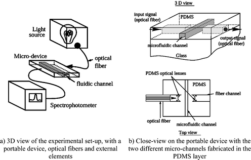 | ||
| Fig. 1 Schematic view of the experimental set-up. | ||
First, this design allows one to put the fiber very close to the microfluidic channel (distance from 50 microns to several hundreds of microns) without any bulge effect. The light is then guided inside the optical fiber with excellent accuracy (losses around 10 dB km−1) and emerges from the fiber near the channel. To improve the excitation efficiency, PDMS 2D optical lenses were also implemented.
The principle of the PDMS lenses can be described as follows. The optical fiber is inserted into the channel ending by a curved interface. The two media on each side of this interface (air and PDMS) possess different refractive indices so that the light beam going through this interface will be deflected, and focused according to the curvature radius of the interface and the incident angle of the light beam.
If we use the coordinate system defined as shown in Fig. 2b, this design cannot modify the light beam along the Z-direction. The efficiency of these lenses is then limited to a 2D plane defined by both the X-axis and Y-axis and parallel to the glass substrate–PDMS layer interface. This design allows the excitation light to be focused onto a specific area in the micro-fluidic channel. A large portion of the optical power launched from the fiber can excite fluorescent response from the sample.
 | ||
| Fig. 2 Characterization of the patterns using a scanning electron microscope. | ||
Therefore, these lenses should drastically increase the sensitivity of this device.
Fabrication process
Many microchips are fabricated using glass or quartz22–23 that do not allow for design flexibility, rapid prototyping and scalable manufacturing. The poly(dimethylsiloxane) material24 is a silicone rubber, which exhibits interesting properties for biological applications, such as biocompatibility, transparency in the visible range, etc. The other advantages of such devices are the low cost and the high reliability.The fabrication process of a PDMS layer can be divided into the following steps: the first step is patterning a mold master onto a glass or silicon substrate, and the second step is molding against the master. By coating and curing PDMS material, the patterned structure on the master can be easily replicated.
To fabricate the mold master, a thick negative photoresist called SU-8 (Micro-Chem Corp, Nano SU-8 50)25–26 is used because of its specific properties. Patterns with a typical thickness varying from a few to several hundred microns can be easily achieved. SU-8 patterns are made using a classic photolithography process as described in ref. 24. By adjusting the parameters (spin-coating speed, etc.), we can fabricate a thick layer with vertical side-walls (see Fig. 2a where a 130 μm thick, 70 μm curvature radius interface is shown).
The PDMS material is well known to replicate perfectly the SU-8 mold, with accuracy around a few tenths of nanometers. A PDMS layer (Sylgard 18424) is then made, reproducing the mold master. Fig. 2b shows the fabricated PDMS layer from the mold master shown in Fig. 2a.
By repeating the second step of the process, this method allows us to fabricate several PDMS layers from the same mold. This material is thus particularly well adapted to fulfill the requirements for industrial applications. Moreover all the steps can be achieved within one day, from the mask to the portable device, therefore this process is also particularly suitable for research and development.
The PDMS layer is then bonded onto a glass substrate (see Fig. 3a) in order to obtain a closed microfluidic channel (the wide channel in the center). On both side of the central channel, the arrays of parallel channels are for optical fiber insertion. The two holes on the lower part of the picture are the inlet and outlet ports, where the sample solution will be introduced into and collected from the channels respectively.
 | ||
| Fig. 3 Photos of the PDMS layer. | ||
The optical fiber is then put inside the channel (see Fig. 3b) as close as possible to the lens and facing the wide microfluidic channel. The central channel for sample solution is 1 mm wide and 130 μm high, and the ones for fiber insertion are 126 μm wide and 130 μm high. For our experiments, the mold master of microfluidic channels and the channels for fiber insertion were fabricated within one photolithography step. The height of all the channels was therefore constant. But SU-8 multi-step fabrication processes27 makes it possible to achieve mold masters with multiple heights.
In order to introduce the fiber into the channels, the typical height of the structure was designed to be around 130 μm. Thus, it was difficult to shorten the distance between the fiber and the microfluidic channel below a few tens of μm, due to the high aspect ratio of such a structure (130 μm in height and a few tens of μm in width). By setting a minimum distance around 50 μm, the peeling off process of PDMS could not be critical and no leakage from the microfluidic channel was observed.
Test of the PDMS lens efficiency
In our experimental set-up, Rhodamine B28 was used as a fluorescent dye to characterize the light beam inside the channels. Therefore, the light coming out from a white lamp was filtered by a narrow band-pass filter centred at 530 nm (green), which corresponds to the maximum of the dye absorption spectrum. The fluorescent emission of the dye is centred around 570 nm (orange). A multimode fiber with a numerical aperture of 0.22, a core diameter of 105 μm, and a clad diameter of 125 μm was used, allowing effective and easy collection of light from the light source. The losses at 500 nm wavelength were estimated around 10 dB km−1, which corresponds to the fact that more than 99.4% of the light power is transmitted per meter.Beam characterization
Systematic studies were carried in order to check the PDMS lens influence on the beam characteristics. The high gain mode was also set on the CCD camera to enhance the contrast and the fluorescent response from the dye. For these experiments, we used the 1 mm wide central microfluidic channel as shown in Fig. 3a.Fig. 4 gives all the details about how we proceeded to extract the two coefficients A and B. These two parameters are useful to compare the beams under different conditions, and then to draw conclusions about the effect of PDMS lenses. These analyses are based on some hypotheses that are detailed below.
 | ||
| Fig. 4 Three steps to define the two different coefficients, the slope A and the constant B. | ||
From the edge of the channel where the dye is flowing, we traced the light intensity profile along the perpendicular direction to the beam symmetry axis every 100 μm (see Fig. 4a). Four of these curves, drawn at 0, 100, 200 and 300 μm away from the border of the channel closer to the lens, are centered and described in Fig. 4b. All the curves exhibit saturation phenomena due to the CCD high gain mode. An arbitrary value was then chosen as reference line (50, or 1/5 of the maximum value) to check the width of the beam. By measuring the beam width on the reference line, several points were obtained and plotted on the same figure versus the distance from the border of the channel (see Fig. 4c).
Up to 300 μm, linear plots were obtained. After that value, and especially for the small curvature radius lens, the non-linear components were quite important and a fit by a linear function was then impossible. In order to keep a simple model, we then limited our study to the first 300 μm inside the microchannel.
Using freeware available on the Internet (Gnuplot29), we then performed a linear regression to determine the two linear coefficients A and B (see Fig. 4d): A corresponds to the slope (divergence of the beam), and B corresponds to the value at the origin (width of the beam at the border of the channel).
Experimental results
The above method was applied to various PDMS lens, and the results are gathered in Fig. 5a and Fig. 5b. | ||
| Fig. 5 Coefficients A and B obtained from a fit by a linear function, versus the PDMS lens curvature radius. | ||
The gray lines on Fig. 5a and Fig. 5b correspond to the reference value obtained with a flat air–PDMS interface at the tip of the fiber channel (no PDMS lens). The line thickness depends on the error bar we found for that parameter.
For coefficient A (slope of the fitting curve), we obtained a beam divergence versus the curvature radius always decreasing, but the slope of the curve tends to decrease gradually. For coefficient B, we obtained a value significantly smaller for 70, 90 and 110 μm than the reference one. But, when the radius is increased, the curve rapidly reaches a limit that corresponds to the reference value. Due to the method used, it was then impossible to see any difference in the values of coefficient B for lens radii bigger than 140 μm. In this study, the flat interface can be considered as a curve interface, with an infinite curvature radius. Parameters A and B obtained with a flat interface can then be understood as asymptotic limits for the two curves. Thus, for the parameter B, this limit is already reached with a 140 μm curvature radius PDMS lens.
Fluorescent emission improvement
Since one of the goals of the study is also to improve the fluorescent response from the dye by optimizing the excitation process, the effect of the PDMS lens on the light emitted by the fluorescent dye was also checked.A CCD camera with normal gain was used in order to avoid the saturation phenomenon that can be seen in the previous figures. For these experiments, the gain of the CCD camera was kept constant in order to enable a comparison of the arbitrary units systems. The light intensity profiles were drawn along a perpendicular axis to the symmetry axis of the light beam, 50 μm away from the border of the channel where the dye was flowing. To draw the light profile, the ‘Scion Image beta 4.02’ freeware30 was used. On two devices, we compared the fluorescent light intensity using several PDMS lenses, with curvature radius R varying from 70 μm to a flat interface (R = 8). The results are presented in Fig. 6a and Fig. 6b.
 | ||
| Fig. 6 Effect of the PDMS lens on the fluorescent light emission from the dye. | ||
Detection limit
In order to check the influence of lenses on the detection limit, systematic studies were carried out with two types of interfaces (70 μm curvature radius and flat interface) and two different distances between the fiber and the microfluidic channel (130 μm and 230 μm). FITC-labelled albumin31 diluted in deionized water was used with concentrations ranging from 1 g l−1 to 0.1 g l−1. The number of FITC molecules attached to one albumin is not precisely determined and varies from 7 to 12. Thus a 1 g l−1 FITC-labelled albumin solution corresponds approximately to a 170 μM FITC solution considering 12 as the ratio of attachment (upper limit).For these experiments, the microfluidic channel was 50 μm in width and 130 μm in height and the gain of the CCD camera was set at 0 dB. The results are presented in Fig. 7.
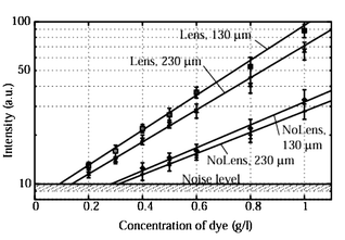 | ||
| Fig. 7 Response of the FITC-labelled albumin flowing inside a microchannel to excitation by an optical fiber: comparison of the design with lens (70 μm curvature radius lens) and without lens (flat air–PDMS interface). The second digit corresponds to the distance between the end of the fiber and the microfluidic channel. | ||
Discussion
Fig. 5 shows that we could slightly adapt the beam properties by just adding a curved interface at the end of the channel in which the optical fiber will be introduced. Two different settings with a small curvature and a medium curvature can be used according to the applications.The small curvature PDMS lenses (typically around 70 μm radius) decrease the width of the beam close to the lens (Fig. 5b). This focusing phenomenon (the spot width is 30% smaller than the flat interface one at the same distance considering Fig. 5) results in improvement of the excitation and emission to around 4 times brighter than the set-up with a flat interface using the same dye concentration (Fig. 6a and 6b).
The effect of such lenses on the detection limit was also checked in order to validate the principle. Fig. 7 shows the four linear curves we obtained depending on the interface shape (with or without 70 μm curvature radius lens) and the distance between the fiber and the microfluidic channel (130 μm and 230 μm).
The upper set of curves corresponds to the design including a PDMS 2D optical lens. Compared to the lower curves (flat interface), the slope is bigger and also the solution with 0.2 gl−1 FITC-labelled albumin diluted into deionized water was clearly detectable. That leads to a detection limit around 0.1 g l−1 of diluted FITC-labelled albumin. Unfortunately, it was impossible to detect this concentration with good accuracy. The detection limit is estimated at around 0.3 g l−1 of diluted FITC-labelled albumin in the case of a flat interface, three times higher than the set-up with small curvature lenses.
If the two upper curves are compared to each other (or the two lower ones), the distance between the fiber end and the microfluidic channel seemed to contribute also to the excitation efficiency. By setting the microfluidic channel 100 μm closer to the fiber, we could slightly improve the detection limit for both configurations.
The use of lenses increased the slope of the linear dependence of the light intensity upon the concentration of fluorescent labels. It should be advantageous for quantitative measurements because the larger slope means increased sensitivity to the concentration.
The other set-up that exhibits non-negligible improvements corresponds to the medium curvature radius PDMS lens (around 160 μm radius). The measurement method could not get any improvement in terms of beam width close to the fiber. But, far from the fiber, the beam divergence is significantly reduced. The light intensity then slowly and progressively decreases as the beam is propagating away. That consideration seems to fulfill the requirements for low concentration absorption measurement. When the concentration of fluorescent species is very low, the length of light path through the fluorescent labeled-protein solution has to be increased in order to achieve detectable absorption.11,20,32
But in the case of absorption measurement set-up, if the light beam divergence is too large, the receiving device will collect only a small part of the light. Including such a lens facing the excitation fiber, we can minimize beam divergence and therefore enhance the coupling between the excitation fiber and the devices to collect the fluorescent emission, e.g. another fiber, waveguide, detector, etc. This set-up should then improve the sensitivity of the absorption based detection method. With our set-up based on an optical fiber with 0.22 numerical aperture, the divergence was decreased by a factor of 2 with a 160 μm curvature radius interface compared to the flat one.
The curves showed in Fig. 5 also demonstrate that the use of lenses can enable one to control the light beam. In terms of fluorescent spectroscopy, it can be applied to avoid a direct coupling effect between the two fibers (excitation and collection) by tilting the two fibers on both sides of the microfluidic channel.
The present 2D optical lens is useless if we consider the Z-direction, perpendicular to substrate surface. This phenomenon, coupled with the roughness of the vertical side wall that we cannot control with a better accuracy than a few tenths of the excitation wavelength going through the lens, could explain the difficulty we had to focus the light beam inside a smaller diameter sphere. The aberration also was not taken into account in this study. These parameters should be carefully considered in order to improve the presented results.
Conclusion
We have presented in this paper a new approach with optical fibers directly inserted into channels that end with PDMS 2D optical lenses. This method exhibits several advantages, such as a cheap microchip with self-aligned fibers put close to the microfluidic channel. The efficiency of these lenses in terms of the fluorescent dye excitation was characterized. The results demonstrate non-negligible improvements compared to the commonly used flat interface, and two set-ups were pointed out in this article in terms of beam divergence and light emission intensity of the fluorescent dye.Considering the case of fluorescent spectroscopy, the 70 μm curvature radius PDMS 2D optical lens exhibits the best properties compared to the same design without any lens. The dye excitation was enhanced by a factor of 4. In terms of sensitivity, these lenses yield a lower detection limit threshold by a factor of 3.
For detection via absorbance, the use of a 160 μm curvature radius is more suitable. It leads a reduction of the light beam divergence by a factor of 2.
The present technique doesn’t require any specific fabrication step and can be easily applied to portable devices based on a PDMS layer and optical fibers. By a slight modification of the photolithography masks, the performance of such devices can be improved in term of excitation efficiency for both absorption and fluorescent measurements.
This design can also be applied to other detection methods, such as UV absorbance since the PDMS material absorption is small from the near UV to the IR wavelength. Depending on the application, to set the right fiber optimised for a certain wavelength is sufficient to adapt the present method to other domains of application.
Acknowledgements
This work was performed in the framework of collaboration among LIMMS/CNRS-IIS at the University of Tokyo and is partially supported by the JSPS (Japanese Society for the Promotion of Science).References
- H. M. Widmer, Trends in industrial analytical chemistry, Trends Anal. Chem., 1983, 2(1), 77–79 CrossRef.
- A. Manz, N. Graber and H. M. Widmer, Miniaturized total chemical analysis systems: a novel concept for chemical sensing, Sens. Actuators B, 1990, 1, 244–248 CrossRef.
- D. J. Harrison, K. Fluri, K. Seiler, Z. Fan, C. S. Effenhauser and A. Manz, Micromachining a Miniaturized Capillary Electrophoresis-Based Chemical Analysis System on a Chip, Science, 1993, 261, 895–897 CAS.
- J. R. Webster, M. A. Burns, D. T. Burke and C. H. Mastrangelo, Monolithic capillary electrophoresis device with integrated fluorescence detector, Anal. Chem., 2001, 73, 1622–1626 CrossRef CAS.
- P. Yang, G. Wirnsberger, H. C. Huang, S. R. Cordero, M. D. McGehee, B. Scott, T. Deng, G. M. Whitesides, B. F. Chmelka, S. Buratto and G. D. Stucky, Mirrorless lasing from mesostructured waveguides patterned by soft lithography, Science, 2000, 287, 465–467 CrossRef CAS.
- J. Hübner, K. B. Mogensen, A. M. Jorgensen, P. Friis, P. Telleman and J. P. Kutter, Integrated optical measurement system for fluorescence spectroscopy in microfluidic channels, Rev. Sci. Instrum., 2001, 72(1), 229–233 CrossRef CAS.
- H. Qiao, S. Goel, A. Grundmann and J. N. McMullin, Fabrication of Micro-Optic/Microfluidic biochips, in Proc. ICAPT 2002 International Conference On Applications Of Photonic Technnology, Quebec, Canada, 2002 Search PubMed.
- S. Ura and S. J. Sheard, A configuration for guided-wave excitation into a disposable integrated-optic head, Opt. Commun., 1998, 146, 85–89 CrossRef CAS.
- C. G. J. Schabmueller, J. R. Pollard, A. G. R. Evans, J. S. Wilkinson, G. Ensell and A. Brunnschweiler, Integrated diode detector and optical fibres for in situ detection within micromachined polymerase chain reaction chips, J. Micromech. Microeng., 2001, 329–333 CrossRef.
- M. L. Chabinyc, D. T. Chiu, J. C. McDonald, A. D. Stroock, J. F. Christian, A. M. Karger and G. M. Whitesides, An integrated fluorescence detection system in Poly(Dimethylsiloxane) for microfluidic application, Anal. Chem., 2001, AC010423Z.
- Z. Liang, N. Chiem, G. Ocvirk, T. Tang, K. Fluri and D. J. Harrison, Microfabrication of a Planar Absorbance and Fluorescence Cell for Integrated Capillary Electrophoresis Devices, Anal. Chem., 1996, 68, 1040–1046 CrossRef.
- D. A. Fletcher, N. U. Webb, S. K. Gordon, C. F. Quate and K. E. Goodson, Thermal Microscopy with a microfabricated solid immersion lens, in Proc. IEEE/LEOS Optical MEMS 2001, Okinawa, Japan, 2001, pp. 157–158 Search PubMed.
- E. M. Strzelecka, G. D. Robinson, L. A. Coldren and E. L. Hu, Fabrication of refractive microlenses in semiconductors by mask shape transfer in reactive ion etching, Microelectron. Eng., 1997, 35, 385–388 CrossRef CAS.
- C. Croutxe-Barghorn, O. Soppera and D. J. Lougnot, Fabrication of microlenses by direct photo-induced crosslinking polymerization, Appl. Surf. Sci., 2000, 168, 89–91 CrossRef CAS.
- H. Jiang, X. Yuan, Z. Yun, Y. C. Chan and Y. L. Lam, Fabrication of microlens in photosensitive hybrid sol–gel films using a gray scale mask, Mater. Sci. Eng. C, 2001, 16, 99–102 Search PubMed.
- K. Naessens, H. Ottevaere, P. Van Daele and R. Baets, Flexible fabrication of microlenses in polymer layers with excimer laser ablation, Appl. Surf. Sci., 2003, in press.
- P. C. Nicolson and J. Vogt, Soft contact lens polymers: an evolution, Biomaterials, 2001, 22(24), 3273–3283 CrossRef CAS.
- J-C. Roulet, R. Völkel, H. P. Herzig, E. Verpoorte, N. F. de Rooij and R. Dändliker, Fabrication of multilayer systems combining microfluidic and microoptical elements for fluorescence detection, J. Microelectromech. Syst., 2001, 10(4), 482–491 CrossRef CAS.
- S. Camou, T. Fujii, J. P. Guoy and H. Fujita, Design of a 2-D optical lens on a PDMS micro-chip to improve fluorescence spectroscopy using integrated optical fibers, in Proc. IEEE/LEOS Optical MEMS 2001, Okinawa, Japan, 2001, pp. 133–134 Search PubMed.
- K. W. Ro, B. C. Shim, K. Lim and J. H. Hahn, Integrated light collimating systems for extended optical-path-length absorbance detection in microchip-based capillary electrophoresis, in Proc. μTAS, ed. J. S. Ramsey and A. VandenBerg, Kluwer Academic Publishers, Dordrecht, 2001, pp. 274–276 Search PubMed.
- J. Seo and L. P. Lee, Integrated microfluidic optical system (iMOS) with LED, in Proc. μTAS, 2002, ed. Y. Baba, S. Shoji and A. VandenBerg, Kluwer Academic Publishers, Dordrecht, pp. 284–287 Search PubMed.
- I. Schneengass and J. M. Kohler, Flow-through Polymerase Chain Reactions in chip thermocyclers, Rev. Mol. Biotechnol., 2001, 82, 101–121 CrossRef.
- Q. Fang, F. R. Wang, S. L. Wang, S. S. Liu, S. K. Xu and Z. Lun, Sequential injection sample introduction microfluidic-chip based capillary electrophoresis system, Anal. Chim. Acta, 1999, 390, 27–37 CrossRef CAS.
- T. Yamamoto, T. Fujii, T. Nojima, J. W. Hong and I. Endo, Cell free protein synthesis in PDMS-glass hybrid microreactor, Proc. SPIE, 2000, 4177, 72–81 Search PubMed.
- H. Lorentz, M. Despont, N. Fahrni, J. Brugger, P. Vettiger and P. Renaud, High-aspect-ratio, ultrathick, negative-tone near-UV photoresist and its applications for MEMS, Sens. Actuators A, 1998, 64, 33–39 CrossRef.
- J. Zhang, K. L. Tan and H. Q. Gong, Characterization of the polymerisation of SU-8 photoresist and its applications in micro-electro-mechanical systems (MEMS), Polym. Test., 2001, 20, 693–701 CrossRef CAS.
- L. Griscom, P. Degenaar, B. LePioufle, E. Tamiya and H. Fujita, Techniques for patterning and guidance of primary culture neurons on micro-electrode arrays, Sens. Actuators B, 2002, 83, 15–21 CrossRef.
- Rhodamine B data sheets are available at this address: omlc.ogi.edu/spectra/PhotochemCAD/html/du98.html.
- Gnuplot freeware is available at this address: www.gnuplot.info.
- Scion freeware is available at this address: www.scioncorp.com.
- Data sheets for FITC fluorescent dye are available at this address: www.sigma.com (product number A9771).
- M. A. Schwarz and P. Hauser, Recent developments in detection methods for microfabricated analytical devices, Lab Chip, 2001, 1, 1–6 RSC.
| This journal is © The Royal Society of Chemistry 2003 |