MEMS technology in analytical chemistry
Anil K.
Deisingh
Department of Chemistry, McMaster University, 1280 Main Street West, Hamilton, Ontario, Canada L8S 4M1. E-mail: deisin@mcmaster.ca
Abstract
Microelectromechanical systems promise to revolutionize nearly every product category by bringing together silicon-based microelectronics with micromachining technology, moving us closer towards the realization of complete systems-on-a-chip. Anil Deisingh talks us through the basics of MEMS technology and the growing role of these new ″micromachines″ in analytical chemistry applications.
Introduction
Microelectromechanical systems (MEMS) combine mechanical parts, sensors, actuators and electronics on a common silicon substrate through the utilization of microfabrication technology.1 It exploits the current developments in microelectronics to create complex machines with sizes in the micrometer range.2 It has been estimated that the market for intelligent micromachine based-systems is about $100 billion per year.2 MEMS technology allows the hybridization of silicon-based microelectronics with micromachining approaches which may allow the development of complete systems-on-a-chip.1 The initial analytical chemistry developments towards integrated systems were first proposed by several groups including those of Manz,3 Harrison4 and Ramsey.5Monocrystalline silicon is the ideal material for MEMS devices. Advantages to its use include that it is stronger than steel, resistant to fatigue, flexible, allows the maintenance of device integrity, allows the fabrication of complex devices and eliminates inter-level interference.6–8 Silicon etching is the most popular method for micromachining although other methods such as lithography, laser machining and mechanical micromachining are also used.9 Further information on these aspects may be obtained from ref. 10.
MEMS are becoming more commonplace in several industries. Commercially, in 2002, the main uses of these devices were in disposable blood pressure sensors, pressure sensors for engines, packaged airbag accelerometers, inkjet printer heads and magnetic heads for computer hard drives.11 Some of the enabling technologies allowed by MEMS include polymerase chain reaction (PCR) microsystems for DNA amplification and identification, micromachined scanning tunelling microscopes (STMs), biochips for the detection of chemical and biological agents and microsystems for high-throughput drug screening and selection.1 These technologies are finding use towards the development of lab-on-a-chip systems. Many more examples will be given later in this paper.
However, in terms of commercialization, MEMS devices can prove risky and costly in high-volume production.11 Furthermore, there is a lack of standards and the technology is fragmented from an engineering perspective.11 Process development is, therefore, a major issue in the production of these devices. Additionally, packaging of these devices can also be a major problem.
Regardless of these concerns, MEMS are finding a growing role in analytical chemistry applications. There are several advantages to the use of these devices including rapid analysis times, portability, decreased consumption of reagents and the possibility for automation of the analysis. To better appreciate the design and operation of these devices, two examples have been chosen for further description.
Fig. 1 shows the schematic of a MEMS device used for an electrochemical immunoassay (ECIA). This system was developed for paramagnetic bead-based ECIAs.12 The microanalysis uses flow-through reaction chambers containing the beads with reagents being passed through. The chamber is a microfabricated component containing an electromagnet to capture beads and electrodes to detect 4-aminophenol (PAP) at an interdigitated array (IDA).
| 4-aminophenol →2H+ + 2e− + 4-quinonemonoimine (PQI) |
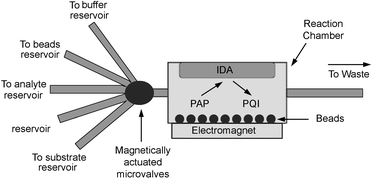 | ||
| Fig. 1 Schematic of the MEMS for ECIA. (Reprinted from N. J. Ronkainen-Matsuno et al., Trends Anal. Chem., 2002, 21, 224. By permission of Elsevier Science.) | ||
Another example of the use of MEMS is shown in Fig. 2. This system is based on a concept proposed by Manz and co-workers.13 It shows a stacked micromachined flow system for adsorptive stripping monitoring of trace metals, based on vertically aligned functional modules, each 2.5 cm2.14 These are stacked upon each other, including the sample and reagent reservoirs, micropumps and flow detector. The sample and reagent are mixed and allowed to react reproducibly.14
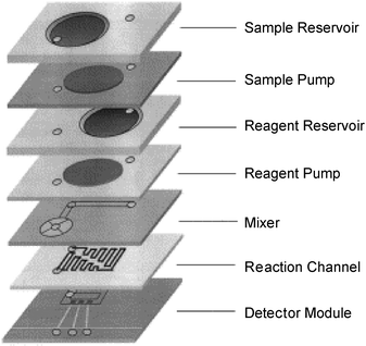 | ||
| Fig. 2 A stacked micromachined flow system for adsorptive stripping monitoring of trace metals. (Reprinted from J. Wang et al., Anal. Chim. Acta, 1999, 385, 429. By permission of Elsevier Science.) | ||
MEMS applications in analytical chemistry
In this section, we will discuss examples of the various uses of MEMS devices. They range from medical applications to imaging technology, environmental uses, development of sensors, integration to mass spectrometers and biological detection.One particularly interesting application is the use of MEMS probes for intracellular recording.15 Multi-site brain recordings of freely behaving animals allow scientists to link neuronal activity with external stimulation and behaviour. This provides a better understanding of the interactions of brain cells.15 MEMS allow microelectrodes to be further miniaturized for neuronal recording and it also allows integrated sensors for multi-site recording to be developed.15 MEMS probes produce improved signal quality compared with the ones currently available.
As expected, MEMS technology has started to become important in the medical field, with several applications being developed. MEMS-based microdelivery of drugs can be used as implantable medical devices. In one case, each drug dose is contained in an individually addressable microreservoir.16 The devices rely on either an electrochemical reaction or biodegradation to remove the reservoir cap after which the active material in the well can dissolve or diffuse into the surrounding solution. In another application, a MEMS flow sensor has been developed to monitor in vitro flow rate measurements of body fluids for haematology and urinalysis.17 This is achieved by measuring the forced convective heat transfer from a thermal sensing element to the fluid, with 10 μL min−1 being the lowest flow rate obtained.
With the completion of the sequencing of the human genome, there is much activity towards the development of automated molecular diagnostics systems. MEMS devices are allowing the achievement of automated sample preparation, cell separation and nucleic acid purification and amplification.18 A major goal of chemists is to perform PCR on a microchip but this process has been fraught with difficulties. Researchers have carried out electrothermal modelling of PCR chips using commercially-available MEMS software (IntelliSuite™) to find an optimum chip structure.19 They have found that that the structure and heater design can make a great impact in reducing the cracks in chips. In a similar manner, Burns′ group in Michigan has been active in developing integrated DNA analysis devices.20
Research into various sensors has been one of the main applications of MEMS. An IR-based sensor for monitoring industrial pollutants such as CO2, CO and NOx has been reported. The design uses silicon-based, thermally isolated bridge structures fabricated by MEMS-based methods.21 Gas detection was by non-dispersive IR techniques with target gas species and concentration determined from comparison with referenced spectra.21 Recently, a blood cell counter sensor based on MEMS has been used to determine the number of blood cells in human blood.22 The aperture-impedance method was used to detect these cells as voltage signals. A bioMEMS device with integrated microdialysis probe and biosensor array for continuous sample and on-line monitoring of glucose has been described. The device was a microdialysis sampling system combined with a flow through channel of a microfabricated enzyme sensor.23
A detection system for E. coli based on MEMS, self-assembled monolayers (SAMs), DNA hybridization and enzyme amplification has been reported in the literature.24 The detector array was made with multiple electrodes deposited on a silicon wafer by MEMS technology. A monolayer of streptavidin was immobilized on to a gold electrode to capture rRNA from E. coli. Detection was carried out amperometrically with results obtained in 40 min and a detection limit of 1000 E. coli cells was reported.
MEMS flow sensors have been utilized for nano-fluidic applications such as measuring liquid flow rates in the nL min−1 range.25 The micromachined sensors use a boron-doped polysilicon thin-film heater embedded in the silicon nitride wall of a microchannel. It has been reported that the sensors can also detect microbubbles in the liquid. In a related development, MEMS force sensors have been used for in situ mechanical characterization of nano-scale thin films in scanning and transmission electron microscopies.26 The microfabrication techniques were used to co-fabricate thin film samples with force sensors so as to obtain small sizes suitable for in situ experiments with SEM or TEM. The authors indicate that this approach allows single or multilayers of material to be deposited on the silicon substrate.
Finally, attempts have been made towards integrating micromachined devices with mass spectrometers. Initial attempts were on optimizing experimental arrangements to produce a stable electrospray.27 Recently, a micromachined, low-cost mass spectrometer has been developed.28 The micromachined device contains the ionisation chamber, the filter and the detector on one chip. The entire manufacturing process was based on MEMS technology and initial results with the instrument indicate its usefulness for helium detection in leaks. A MEMS-based approach to the fabrication of microfluidic devices has demonstrated the possibility of using a microfabricated nozzle structure for the nanoelectrospray of solutions for high-throughput mass spectrometry.29 The authors of the paper indicate that 3 samples per minute may be analyzed.
Conclusion
In this paper, we briefly examined the concepts behind MEMS technology and gave several examples of MEMS devices in chemistry. MEMS-based instrumentation can provide miniaturization and automation and, although there are several problems still to be solved, the technology may be harnessed to considerably reduce analysis times and even lead to the production of the elusive ‘lab-on-a-chip’. Readers interested in further information on the lab-on-a-chip can consult refs. 18 and 30.Acknowledgements
I would like to thank Professor Michael Thompson of the University of Toronto for helpful suggestions and advice. The reviewer is also thanked for providing many useful ideas and comments which allowed the paper to be improved.References
- http://www.mems-exchange.org/MEMS/what-is.html .
- http://www.sandia.gov/mstc/technologies/micromachines/vision.html .
- A. Manz, N. Graber and H. M. Widmer, Sens. Actuators, B, 1990, 244.
- A. Manz, J. C. Fettinger, E. Verpoorte, H. Ludi, H. M. Widmer and D. J. Harrison, Trends Anal. Chem., 1991, 10, 144 CrossRef CAS.
- S. C. Jacobson, R. Hergenroder, A. W. Moore and J. M. Ramsey, Anal. Chem., 1994, 66, 144.
- http://www.sandia.gov/mstc/technologies/micromachines/micromachine.html .
- J. W. Gardner, Microsensors, MEMS and Smart Devices, Wiley, Chichester, 2001 Search PubMed.
- T.-R. Hsu, MEMS and Microsystems: Design and Manufacture, McGraw-Hill, Boston, 2002 Search PubMed.
- http://www.lab-on-a-chip.com/publications/evalrev3.htm .
- V. K. Varadan, Proc. SPIE-Int. Soc. Opt. Eng., 2001, 4591, 28 Search PubMed.
- J. DeGaspari, Mech. Eng., 2002, 38 Search PubMed.
- N. J. Ronkainen-Matsuno, J. H. Thomas, H. B. Halsall and W. R. Heineman, Trends Anal. Chem., 2002, 21(4), 213 CrossRef CAS.
- E. Verpoorte, B. H. van der Schoot, S. Jeanneret, A. Manz, H. M. Widmer and N. F. de Rooij, J. Micromech. Microeng., 1994, 4, 246 CrossRef CAS.
- J. Wang, Trends Anal. Chem., 2002, 21(4), 226 CrossRef CAS.
- Y. Hanein, K. F. Bohringer, R. C. Wyeth and A. O. D. Willows, Sens. Update, 2002, 10, 47 Search PubMed.
- R. Scheidt, A. Richards, A. Rosenberg, A. Johnson, G. Voskerician, J. Anderson, R. Langer and M. J. Cima, Proceedings of the 28th International Symposium on Controlled Release of Bioactive Materials, 2001, vol. 1, p. 59 Search PubMed.
- E. Meng, S. Gassmann and Y.-C. Tai, Proceedings of the μTAS 2001 Symposium, Kluwer, The Netherlands, 2001, p. 167 Search PubMed.
- Y. Huang, E. L. Mather, J. L. Bell and M. Madou, Anal. Bioanal. Chem., 2002, 372(1), 49 Search PubMed.
- Z. Cui, Z. Zhao and S. Xia, Proc. SPIE-Int. Soc. Opt. Eng., 2001, 4407, 275 Search PubMed.
- M. A. Burns, B. N. Johnson, S. N. Brahmasandra, K. Handique, J. R. Webster, M. Krishnan, T. S. Sammarco, F. P. Man, D. Jones, D. Heldsinger, V. Namasivayam, C. H. Mastrangelo and D. T. Burke, Science, 1998, 282, 484 CrossRef CAS.
- J. T. Daly, D. Choi, E. A. Johnson, N. Moelders, M. P. McNeal, M. U. Pralle, A. C. Greenwald, W. Ho, I. Puscasu and T. George, Proc. SPIE-Int. Soc. Opt. Eng., 2002, 4576, 49 Search PubMed.
- D. Satake, H. Ebi, N. Oku, K. Matsuda, H. Takao, M. Ashiki and M. Ishida, Sens. Actuators, B, 2002, B83(1–3), 77 CrossRef.
- P. S. Petrou, I. Moser and G. Jobst, Biosens. Bioelectron., 2002, 17, 859 CrossRef CAS.
- J. Gau, Jr, E. H. Lan, B. Dunn, C.-M. Ho and J. C. S. Woo, Biosens. Bioelectron., 2001, 16, 745 CrossRef.
- S. Wu, Q. Lin, Y. Yuen and Y.-C. Tai, Sens. Actuators, A, 2001, A89(1–2), 152 Search PubMed.
- M. A. Haque and M. T. A. Saif, Sens. Actuators, A, 2002, A97–98, 239 Search PubMed.
- P. A. Limbach and Z. Meng, Analyst, 2002, 127, 693 RSC.
- N. Sillon and R. Baptist, Sens. Actuators, B, 2002, B83(1–3), 129 CrossRef.
- T. N. Corso, C. K. Van Pelt, S. Zhang, S. J. Prosser and G. A. Schultz, Proc. SPIE-Int. Soc. Opt. Eng., 2001, 4265, 81 Search PubMed.
- G. H. W. Sanders and A. Manz, Trends Anal. Chem., 2000, 19, 364 CrossRef CAS.
| This journal is © The Royal Society of Chemistry 2003 |