CMOS-based chemical microsensors
Andreas
Hierlemann
* and
Henry
Baltes
Physical Electronics Laboratory, ETH Zurich, Hönggerberg, HPT H 4.2, CH-8093 Zurich, Switzerland. E-mail: hierlema@iqe.phys.ethz.ch; Fax: +41 1 633 1054; Tel: +41 1 633 3494
First published on 4th December 2002
 Andreas Hierlemann Andreas Hierlemann | Andreas Hierlemann received a Diploma in Chemistry in 1992 and a PhD in Physical Chemistry in 1996 from the University of Tübingen, Germany. After working as a Postdoc at Texas A&M University, College Station, TX (1997), and Sandia National Laboratories, Albuquerque, NM (1998), he moved to ETH Zurich in Switzerland where he is currently a member of the technical staff. The focus of his research activities is on CMOS transducers, chemical sensors and interfacial design. |
 Henry Baltes Henry Baltes | Henry Baltes received a DSc degree from ETH Zurich in 1971. He has held faculty positions at Freie Universität Berlin and University of Düsseldorf, Germany, University of Waterloo, Canada and EPF Lausanne, Switzerland. He worked for Landis & Gyr Zug, Switzerland (1974–1982), directing the Solid-State Device Laboratory; he held the Henry Marshall Tory Chair at the University of Alberta, Edmonton, Canada (1983–1988), where he directed a research program in microsensors; he was a Director of LSI Logic Corporation of Canada (1986–1988), and since 1988 he has been Professor of Physical Electronics at ETH Zurich and Director of the Physical Electronics Laboratory active in silicon integrated micro-systems. |
1 Introduction
The rapid development of integrated circuit (IC) technology during the past decades has initiated many initiatives to fabricate chemical sensors on silicon or CMOS substrates (CMOS: Complementary Metal Oxide Semiconductor).1,2 The largely two-dimensional integrated circuit and chemical sensor structures processed by combining lithographic, thin film, etching, diffusive and oxidative steps have been recently extended into the third dimension using micromachining or MEMS (MEMS: MicroElectro-Mechanical Systems) technologies—a combination of special etchants, etch stops and sacrificial layers.3–9 A variety of micromechanical structures including cantilever beams, suspended membranes, freestanding bridges, etc. have been produced.3–9 The realization of microelectronics and micromechanics (MEMS-structures) on a single chip allows for on-chip control and monitoring of the mechanical functions as well as for data preprocessing such as signal amplification, signal conditioning, or data reduction.3–12CMOS- or CMOS-MEMS-technology, therefore, provides excellent means to meet some of the key criteria of chemical sensors such as miniaturization of the devices, low power consumption, rapid sensor response characteristics, or batch fabrication at industrial standards and low costs. Additional advantages come from the possibility of monolithic co-integration of circuitry and transducers. These include improved sensor signal-to-noise characteristics due to on-chip signal processing and analog/digital conversion, or the realization of smart features on the sensor chip. Drawbacks of using CMOS technology encompass a limited selection of materials (see CMOS technology section) and a predefined fabrication process for the CMOS part. Sensor-specific or transducer-specific materials and fabrication steps have to be introduced as post-processing after the CMOS fabrication.13
After a short introduction to CMOS and basic micromachining technologies, we will give an overview on different types of chemical sensors fabricated in CMOS and CMOS-MEMS technology.
2 CMOS technology
CMOS is the dominant semiconductor technology for microprocessors, memories and application-specific integrated circuits (ASICs).14–16 CMOS-chips generally consist of a layered structure of aluminum, polysilicon, silicon (doped and undoped), silicon oxide and -nitride layers (Fig. 1), which are fabricated in a defined sequence of material deposition, doping, lithography and etching steps.14–16 | ||
| Fig. 1 Cross-section of a CMOS-chip. The different layers and materials include metals (aluminum), silicon oxides, silicon nitride, and polysilicon on a p-doped silicon wafer with n-well implanted areas. | ||
Semiconductors conduct electricity but not enthusiastically. Semiconductor areas that are doped become conductors of either extra electrons with a negative charge (phosphorus-doping) or of positive charge carriers (boron-doping). The denomination ‘complementary’ metal oxide semiconductor is due to the fact that both, n-type and p-type transistors are realized on the same substrate, for example on a lightly p-doped wafer material, that exhibits n-doped areas (n-wells) (Fig. 1). Both, n-type (NMOS) and p-type (PMOS) transistors are used to realize logic functions. A CMOS-chip cross-section is shown in Fig. 1. The p-substrate exhibits n-well areas created by implantation. Heavily p-doped structures (p+) in the n-well, and n-doped structures (n+) in the p-substrate form transistor source and drain. The transistor gate is made of polysilicon on top of the gate oxide (SiO2). By applying a voltage to the gate via the polysilicon, electrons or holes are accumulating in the surface area (field effect) below the gate and thus create a conducting n- or p-channel between source and drain. Variation of the gate voltage thus modulates the source drain current: continuously within a certain range in analog circuits, on/off in digital circuits. Several metal layers (Fig. 1: metal 1 and metal 2, aluminum) are used to wire the transistors. Dielectric layer such as field oxide, contact oxide, and intermetal oxide (SiO2) serve as electrical insulation between conducting areas. The silicon nitride on top serves as passivation and provides electrical and mechanical/chemical protection of the circuitry. Silicon nitride and to a lesser extent silicon oxide (or silicon with a native oxide layer) are durable in case of liquid exposure and are biocompatible, which allows for using CMOS chips also with cells or living material. CMOS aluminum is neither stable in liquids (or in air at higher temperatures) nor is it biocompatible, and, consequently, has to be covered with precious metal coatings such as gold or platinum. For more details on semiconductor technology, see, e.g., the standard textbooks of Sze.15,16
3 Micromachining techniques
3.1 Bulk micromachining
One approach to enhance the functionality of IC-based substrates includes micromachining the bulk substrate, which in most cases consists of silicon. Silicon can be dry or wet etched by various techniques.3–7,17 Some wet etchants such as nitric acid/hydrofluoric acid lead to isotropic etching (same etch rate in all directions), others like potassium hydroxide lead to anisotropic etching, i.e., preferentially etch away the silicon along certain crystal planes while preserving it in other directions (Fig. 2a). Typical structures obtained by, e.g., anisotropic wet etching through the complete bulk silicon of a CMOS wafer include membranes consisting of the remaining dielectric CMOS layers. The thermal oxide serves as an etch-stop layer. The resulting membrane structures can be used for sensors requiring excellent thermal insulation, such as calorimetric chemical sensors or metal oxide-covered microhotplates. | ||
| Fig. 2 Micromachining techniques: (a) bulk micromachining, anisotropic and isotropic etching, (b) surface micromachining with sacrificial layer, structural layer and a subsequent etch step. | ||
Another technique is dry etching. Again, there is isotropic etching performed by using, e.g., xenon difluoride or anisotropic etching by reactive-ion-etching (RIE). RIE can be used to release cantilevers or create bridge structures from preformed membranes.18
3.2 Surface micromachining
Surface micromachining comprises a number of techniques to produce microstructures from thin films previously deposited onto a substrate and is based on a sacrificial layer method (Fig. 2b). In contrast to bulk micromachining, surface micromachining leaves the substrate intact. A sacrificial layer is deposited and patterned on a substrate. After that, a structural thin film, in most cases polysilicon, is deposited and patterned, which will perform the mechanical or electrical functions in the final device. A selective etchant then removes exclusively the sacrificial layer material. The thickness of the sacrificial layer determines the distance of the structural parts from the substrate surface. Common sacrificial layer materials include silicon oxide etched by hydrogen fluoride and aluminum etched by a mixture of phosphoric, nitric and acetic acid.Clamped beams, microbridges, or microchannels can be fabricated this way, microrotors and even microgears can be realized by repeated layer deposition and etching.3–7,17
4 CMOS-based chemical sensors
Chemical sensors usually consist of a sensitive layer or coating and a transducer.19–25 Upon interaction with a chemical species (absorption, chemical reaction, charge transfer etc.), the physicochemical properties of the coating, such as its mass, volume, optical properties or resistance etc. reversibly change. These changes in the sensitive layer are detected by the respective transducer and translated into an electrical signal such as frequency, current, or voltage, which is then read out and subject to further data treatment and processing.A variety of transducers based on different physical principles have been devised. We will follow a classification scheme suggested by Janata20,21 to give an overview on CMOS-based chemical sensors in the next sections of this review. This scheme includes four principal categories distinguished with regard to the transduction principle:20
1. Chemomechanical or mass-sensitive sensors (e.g., mass changes due to absorption)
2. Thermal sensors (e.g., temperature changes through chemical interaction)
3. Optical sensors (e.g., light intensity change by absorption)
4. Electrochemical sensors (e.g., potential or resistance changes through charge transfer)
We will briefly introduce each of those four sensor categories and then give examples of CMOS-based transducers and devices. Typical chemically sensitive materials and sensor applications will be mentioned in the context of the corresponding transducer structures.
4.1 Chemomechanical or mass-sensitive sensors
Chemomechanical or mass-sensitive sensors are in the simplest case gravimetric sensors responding to the mass of species accumulated in a sensing layer.26–28 Some of the sensor devices additionally respond to changes in a variety of other mechanical properties of solid or fluid media in contact with their surface such as changes of polymer elastic moduli, liquid density and viscosity,26–28 which will not be further discussed here. Chemomechanical sensor, therefore, is a more appropriate denomination. Any species that can be immobilized on the sensor can, in principle, be sensed. As with most of the chemical sensors, the measurements are taken at a thermodynamic equilibrium state.Mass changes can be monitored by either deflecting a micromechanical structure due to stress changes or mass-loading (static measurements) or by assessing the frequency changes of a resonating structure or a traveling acoustic wave upon mass loading. Both deflection and resonance frequency change in proportion to stress changes or mass loading on the device.26–28
The most common devices are the thickness shear mode resonator (TSMR) or quartz microbalance (QMB), and the Rayleigh surface acoustic wave (SAW) device, both based on piezoelectric quartz substrates. Both will not be detailed here, since they are not fabricated in CMOS technology. For more details on those devices, see refs. 26–28.
In the following, we will describe in more detail two CMOS-technology-based micromechanical structures for mass-sensitive devices, (1) flexural-plate-wave devices (FPWs), and (2) micromachined cantilevers.
 | ||
| Fig. 3 Schematic of a flexural plate wave device. The side view shows the different layers and the membrane movement. Interdigitated electrodes are used for actuation. | ||
The interdigital transducers (IDTs) on these devices generate flexural waves (Lamb waves, Fig. 3) with retrograde elliptical particle motions as in the SAW devices. The Lamb waves give rise to a series of plate modes, one of which has a frequency that is much lower than those of the other possible modes. The velocity of this unique wave decreases with decreasing plate thickness. The entire thickness of the plate is set in motion like the ripples in a flag.26–32 The confinement of acoustic energy in the thin membrane results in a very high mass sensitivity. Since the Lamb wave causes an elliptical particle movement at the transducer surface (Fig. 3), the sensitive films are deformed. The sensitive layer can be deposited on either side of the membrane. Deposition on the backside (non-processed side of the wafer) has the advantage, that on-chip-circuitry will not be exposed to chemicals.29–32
Fabrication sequences for monolithic integration of the Lamb device with CMOS electronics are detailed in refs. 32 and 33.
A variant includes a magnetical FPW actuation scheme based on Lorentz forces: A metal meander-line is patterned on the membrane surface, alternating current (AC) is flowing in the meander transducer and interacts with a static in-plane magnetic field to generate time-varying Lorentz forces, which in turn deform the membrane. Magnetic actuation requires an externally applied magnetic field, but eliminates the need for a piezoelectric layer.34,35 Such layers frequently contain elements (Zn etc.) that pose contamination problems in IC fabrication.34
Typical FPW applications include the detection of different organic volatiles in the gas phase by using polymeric layers,31,35,36 or the use of an FPW-based immunoassay for the detection of breast cancer antigens.37
There are two fundamentally different operation methods: (a) static mode: measurement of the cantilever deflection upon stress changes or mass loading by means of, e.g., a laser via laser light reflection on the cantilever;38–41 (b) dynamic mode: excitation of the cantilever in its fundamental resonance mode and measurement of the frequency change upon mass loading42–46 in analogy to other mass-sensitive transducers. Method (a) requires long and soft cantilevers to achieve large deflections, whereas method (b) requires short and stiff cantilevers to achieve high operation frequencies. Resonators are characterized by their quality factor (Q-factor), which is defined as the ratio of the resonance frequency and resonator bandwidth: the higher the Q-factor, the better the frequency stability of the resonator. The dynamic mode (b) is preferable with regard to simplicity of the measurement configuration since there is no need for an optical setup to determine small cantilever deflection by means of, e.g., laser light reflection.42–46 Method (a) can also be used in liquid media.39,41 The excitation of the resonant cantilever is performed by applying piezoelectric materials (ZnO)47 or by relying on Lorentz forces in a magnetic actuation scheme, which is analogous to that already described in the context of the FPWs: one or several conductor loops are patterned along the cantilever edges, AC is flowing in the loops and interacts with a static in-plane magnetic field to generate time-varying Lorentz forces, which deflect the cantilever.48,49 Another actuation variant includes making use of the different temperature coefficients or mechanical stress coefficients of the cantilever layer materials (bimorph effect).43–46 The different materials give rise to a cantilever deflection upon heating or applying mechanical forces. Cantilever deflection or resonance frequency changes can be detected by embedding piezoresistors in the cantilever base.41–46 The absolute mass resolution of the cantilevers is in the range of a few picograms.38–46 This high mass-sensitivity does not necessarily imply an exceptionally high gas sensor sensitivity since the area coated with the sensitive layer (on the order of 100 × 150 μm), and hence the overall sorption matrix volume is very small.43
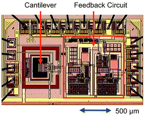 | ||
| Fig. 4 Micrograph of a 150 μm-long CMOS-integrated cantilever with on-chip feedback circuitry. | ||
Fig. 4 shows a CMOS-based cantilever, which is monolithically integrated with feedback electronics.43 The 150 μm-long cantilever consists of mainly silicon as well as vapor-deposited and thermal oxide. The bimorph effect is used to initiate a cantilever vibration by periodically applying electric pulses to heating resistors embedded at the cantilever base. The cantilever resonates at its fundamental mechanical frequency of 380 kHz with a quality factor of approximately 1000 in air, which is comparable to other acoustic-wave-based devices such as QMB or Rayleigh SAW-device. The Q-factor of the cantilever sandwich is dependent on the cantilever materials with silicon offering very favorable properties in comparison to silicon oxide, nitride or the polymer coating.43 The cantilever vibration is detected by embedded piezoresistors in a Wheatstone-bridge configuration. The cantilever acts as the frequency-determining element in a feedback oscillation circuit, which for the first time was entirely integrated on the chip with a counter. The advantages of the monolithic integration here include a better frequency stability of the resonator and lower crosstalk (thermal and electrical) of the different components leading to a better signal-to-noise ratio of the overall system. For more details on the electronics, see refs. 43–46 and 50.
Typical cantilever applications include the detection of organic volatiles or humidity in the gas phase by using polymeric layers,41–46,49–55 and biosensing in liquid phase such as the detection of cells,56 or complementary strands of oligonucleotides (DNA fragments).39
4.2 Thermal sensors
Calorimetric or thermal sensors rely on determining the presence or concentration of a chemical by measurement of an enthalpy change produced by the chemical to be detected.19,20,57 Any chemical reaction or even absorption/desorption process releases or absorbs from its surroundings a certain quantity of heat. Reactions liberating heat are termed exothermic, reactions abstracting heat are termed endothermic. This thermal effect shows a transient behavior: continuous liberation/abstraction of heat occurs only as long as the reaction proceeds. However, there will be no heat production and hence no measurable signal at thermodynamic equilibrium (ΔG = 0) in contrast to mass-sensitive, optical, or electrochemical sensors (see Fig. 15 later).Conflicting constraints are imposed on the design of a thermal sensor. The sensor has to interact with the chemical species (exchange of matter) and thus constitute a thermodynamically open system, but at the same time the sensing area should be thermally as isolated as possible to achieve maximum sensitivity.
The liberation or abstraction of heat can be conveniently measured as a change in temperature, which then is transduced into an electrical signal. The various types of calorimetric sensors differ in the way that the evolved heat is transduced.19,20,57
The catalytic sensor (often denoted ‘pellistor’58) employs platinum resistance thermometry, while the thermoelectric sensor is based on the Seebeck effect.57 Both sensor types benefit from CMOS integration and will be detailed in the following sections.
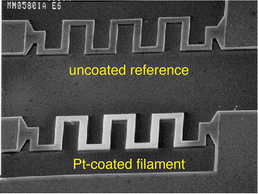 | ||
| Fig. 5 Micrograph (SEM) of two meandered polysilicon filaments. The lower filament is coated with a thin (approx. 0.1 μm) layer of platinum (CVD). In a differential gas sensing mode, the upper, uncoated, filament acts to compensate changes in the ambient temperature, thermal conductivity and flow rate. Reprinted from ref. 59 with permission. | ||
Fig. 5 shows a surface-micromachined, free-standing, Pt-coated polysilicon micro-filament (10 μm wide, 2 μm thick) separated from the substrate by a 2 μm air gap.59,60 Other designs include micromachined membranes.61–66 Heat losses to the silicon frame are minimized in both designs. By passing an electric current through the meander, the microfilament is heated to a temperature sufficient for the Pt-surface to catalytically oxidize the combustible mixture; the heat of oxidation is then measured as a resistance variation in the Pt. The combustion of, e.g., methane generates 800 kJ mol−1 heat, which translates into a corresponding temperature change.
Detailed processing sequences for microbridges are given in refs. 67 and 68.
Typical applications include monitoring and detection of flammable gas hazards such as methane,64,68 hydrogen,59–61,64 propane,61 or carbon monoxide61,65 in industrial, commercial and domestic environments at concentrations below the lower explosive limit (LEL). The LEL is the concentration of gas in air below which it cannot be ignited.
Fig. 6 displays the schematic of a CMOS-based thermopile consisting of a dielectric membrane with polysilicon/aluminum thermocouples (Seebeck coefficient: 111 μV K−1).46,72,73 CMOS-based thermoelectric sensors are advantageously set up in a sensor/reference configuration. The system includes two membranes, one of which is coated with the gas-sensitive polymer, the uncoated one serves as a reference to compensate for gas-induced temperature fluctuations.73 The sensing and reference thermopiles are connected in parallel to the input stage of a low-noise chopper-stabilized instrumentation amplifier on-chip to record the temperature differences between the two membranes. The thermovoltage can be translated into a digital signal on chip using a Sigma–Delta analog/digital converter.74
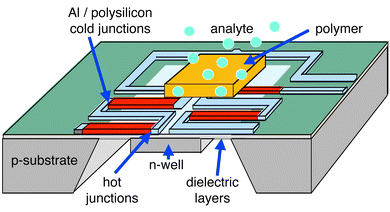 | ||
| Fig. 6 Schematic of a thermoelectric sensor. Polysilicon/aluminum thermopiles are used (hot junctions on the membrane, cold junctions on the bulk chip) to record temperature variations caused by analyte sorption in the polymer. | ||
Processing sequences for the integration of thermoelectric sensors with circuitry in a CMOS standard process are detailed in refs. 72 and 75.
Typical applications include the detection of different kinds of organic volatiles in the gas phase by using polymeric layers,46,72–77 and the biosensing of glucose, urea and penicillin in the liquid phase by using suitable enzymes.71,78–80
4.3 Optical sensors
In comparison to other chemical sensing methods, optical techniques offer a great deal of selectivity already inherent in the various transduction mechanisms. Characteristic properties of the electromagnetic waves such as amplitude, frequency, phase, and/or state of polarization can be used to advantage.81–83 Geometric effects (scattering) can provide additional information. The wavelength of the radiation, e.g., can be tuned to specifically match the energy of a desired analyte-specific resonance or absorption process. In addition, optical sensors like any other chemical sensor can capitalize on all the selectivity effects originating from the use of a sensitive layer.81–83If a sample is irradiated with visible light or electromagnetic waves, the radiation can be absorbed (intensity decrease), scattered (direction randomization, possibly frequency changes), refracted or reflected (metallic reflection, internal reflection mediated by evanescent waves) at the interface(s), or can produce phosphorescence/fluorescence (absorption–emission process) and chemiluminescence (conversion of chemical energy into light) effects.81–83
The generation of light in CMOS or silicon devices is very difficult since there is no first order transition from the valence band to the conduction band without the involvement of a phonon (lattice vibrations).15 However, direct-bandgap semiconductors (III–V-semiconductors) like gallium arsenide (GaAs) or indium phosphide (InP) show first-order radiative electron-hole-recombinations with high quantum efficiency.15 The detection of light is possible with either silicon-based devices (photodiodes) or other semiconducting materials (GaAs, InP). Consequently, integrated optical sensors and systems nowadays mostly are made of III–V-semiconductors, which will not be detailed here, but offer the opportunity for fabrication and integration of lasers, waveguides, phase modulators and detectors on the same chip.84 There is also a wealth of fiber-optical techniques and integrated optical devices, which are realized on silicon substrates without making use of CMOS technology. For details, see review articles.81–83, 85–88
In this article we will exclusively focus on CMOS-based optical sensors, an example of which includes an integrated device making use of bioluminescence.
The integrated circuit detects, processes, and reports the magnitude of the optical signal.89–91 The microluminometer uses the p-diffusion (source and drain diffusions of p-channel MOSFETs, PMOS, Fig. 1) in the n-well as the photodiode. The shallow p-diffusion has a strong response to the 490 nm bioluminescent signal. The entire sensor including all signal processing and communication functions can be realized on a single chip. The integrated circuit contains the devices and circuits to detect the optical signal, to distinguish the signal from noise, to perform analog or digital signal processing, to communicate the results, and to perform auxiliary functions such as temperature assessment or position measurement (Fig. 7).89–91
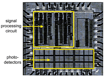 | ||
| Fig. 7 Micrograph of a bioluminescent bioreporter integrated circuit (BBIC). The circuitry blocks are in the upper part, the photodetectors in the lower part of the chip. Reprinted from ref. 90 with permission. | ||
Many types of bioluminescent transcriptional gene fusions have been used to develop light-emitting bioreporter bacterial strains to sense the presence, bioavailability, and biodegradation of different kinds of pollutants. The cells here were entrapped on the chip by encapsulation in natural or synthetic polymers providing a nutrient-rich hydrated environment.89–91
Applications include chemical analysis in gas or liquid phase. Depending on the integration time of the device, trace amounts of toluene and naphthalene were detected in the gas phase using engineered cell colonies of Pseudomonas putida.89–91
Similar CMOS-based photodiode or phototransistor structures such as CMOS charge-coupled detector (CCD) imagers have been used to develop microspectrometers for biochemical analysis92,93 or smart optical sensor systems to measure light intensity and color.94,95 Fabry–Perot-based single-chip microspectrometers (16 addressable Fabry–Perot etalons) that can be used, e.g., for chemical analysis are detailed in refs. 95 and 96.
4.4 Electrochemical sensors
Electrochemical sensors constitute the largest and oldest group of chemical sensors. Many of them are commercially available. Electrochemical sensors make use of electrochemical or charge-transfer reactions, i.e., charge transfer from an electrode to a solid or liquid sample phase or vice versa. Chemical changes take place at the electrodes or in the probed sample volume, and the resulting charge or current is measured. Electrode reactions and charge transport in the sample are both subject to changes by chemical processes (analyte exposure) and hence at the base of electrochemical sensing mechanisms.19–25,97An electrochemical sensor is always composed of at least two electrodes with two electrical connections: one through the probed sample, the other via transducer and measuring equipment. The charge transport in the sample can be ionic, electronic or mixed, while that in the transducer branch is always electronic.
Electrochemical sensors are usually classified according to their electro-analytical principles.20,21,24Voltammetric sensors are based on the measurement of the current–voltage relationship. A potential is applied to the sensor, and a current proportional to the concentration of the electro-active species of interest is measured (amperometry is a special case of voltammetry, where the potential is kept constant). Potentiometric sensors are based on the measurement of the potential at an electrode at equilibrium state, i.e., no current is allowed to flow during the measurement. The measured potential is proportional to the logarithm of the concentration of the electro-active species (Nernst-equation). Conductometric sensors are based on the measurement of a conductance by applying an AC potential with small amplitude to a pair of electrodes in order to prevent polarization. The presence of charge carriers determines the sample conductance.
Another method of classification is according to electronic components.6,25 There are chemoresistors, chemocapacitors and chemotransistors. We will use the electroanalytical principles as the superordinated scheme and use the component notation within the different sections. We will restrict to CMOS-based systems and omit a wealth of literature on other electrochemical sensor designs, for details of which we refer to literature.19–25,97–99
The measured current at any given potential difference depends on the material properties, the composition and geometry of the electrodes, the concentration of the electro-active species (presumably the target analyte) and the mass transport mechanisms in the analyte phase.20,24,97 Among those are migration, the movement of charged particles in an electric field, convection, the movement of material by forced means like stirring or from density or temperature gradients, and diffusion, the movement of material from high-concentration regions to low-concentration regions. The electrochemical reactions at the electrodes are normally fast in comparison to the transport and supply mechanisms. Since convection in the electrode vicinity is avoided, and migration is suppressed by, e.g., a large excess of electro-inactive salts (at the respective potential), diffusion is normally regarded to be the dominant mechanism. There are two components to the measured current, a capacitive component resulting from redistribution of charged and polar particles in the electrode vicinity and a component resulting from the electron exchange between the electrode and the redox species (analyte) termed faradaic current.20,24,97 The faradaic component is the important measurand and is in case of diffusion-limited conditions directly and linearly proportional to the target analyte concentration.20,24
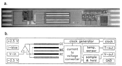
A picture and a schematic of a CMOS-based 3-electrode voltammetric/amperometric sensor is shown in Fig. 8.100 The monolithic device includes the electrochemical sensor, a temperature sensor, and interface circuitry. The circuitry contains an operational amplifier as potentiostat, a switched-capacitor current-to-voltage converter and a clock generator. Interface circuitry and temperature sensor are realized in 3 μm CMOS technology.100 The circuit operates at a supply voltage of ±2.5 V, can apply voltages from +1 V to −1 V to the sensor and handles current ranges from 30 nA full scale to 1 μA full scale. The output voltage of the temperature sensor is proportional to the absolute temperature and has a sensitivity of 125 μV K−1. The total sensor dimensions are 0.75 × 5 mm. Sensor processing sequences are given in refs. 97, 100, 101 and 102. The reference electrodes in liquid phase are in most cases silver/silver chloride elements.
 | ||
| Fig. 8 Micrograph (a) and layout (b) of a CMOS-based 3-electrode amperometric sensor. Reprinted from ref. 100 with permission. | ||
Typical applications include chemical analysis in gas or liquid phase. Target analytes in the gas phase include oxygen101 and carbon dioxide using liquid electrolytes.103 Target analytes in liquid phase comprise dissolved oxygen,100,102,104 glucose,100,105–107 or metal ions.108,109 If the target analyte is not an electro-active species like the glucose molecules monitored with the integrated system here, polymer electrolytes or enzymes (glucose oxidase) producing analyte-related ionic species are used in the sensitive electrode coatings.
The MOSFET (metal oxide semiconductor-FET) as used for chemical gas sensing (Fig. 9) has a p-type silicon substrate (bulk) with two n-type diffusion regions (source and drain). The structure is covered with a silicon dioxide insulating layer on top of which a metal gate electrode (electronics: poly-Si gate) is deposited.
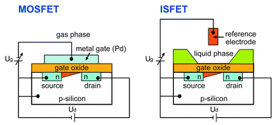 | ||
| Fig. 9 Schematic representation of a MOSFET and an ISFET structure. Ug denotes the gate voltage, Ud the source-drain voltage. The ISFET is realized by replacing the metal gate of the MOSFET with an ionic solution and a reference electrode immersed into this solution. | ||
When a positive voltage (with respect to the silicon) is applied to the gate electrode, electrons, which are the minority carriers in the substrate, are attracted to the surface of the semiconductor. Consequently, a conducting channel (n-channel) is created between the source and the drain, near the silicon dioxide interface. The conductivity of this channel can be modulated by adjusting the strength of electrical field between the gate electrode and the silicon, perpendicular to the substrate surface.
Palladium-(Pd)-gate FET structures were demonstrated to function as a hydrogen sensor by Lundström et al.111 Hydrogen molecules readily absorb on the gate metal (platinum, iridium, palladium) and dissociate into hydrogen atoms. These H-atoms can diffuse rapidly through the Pd and absorb at the metal/silicon oxide interface partly on the metal, partly on the oxide side of the interface.112,113 Due to the absorbed species and the resulting polarization phenomena at the interface, the drain current (Id) is altered and the threshold voltage (Ud) is shifted. The voltage shift is proportional to the concentration or coverage of hydrogen at the oxide/metal interface. Sensitivity and selectivity patterns of gas-sensitive FET devices hence depend on the type and thickness of the catalytic metal used, the chemical reactions at the metal surface, and the device operation temperature.
CMOS-based MOSFETs detecting hydrogen have been described in refs. 114–116.
MOSFET-sensor applications also include the detection of ammonia,112,113 amines, and any kind of molecule that gives rise to polarization in a thin metal film (hydrogen sulfide, ethene etc.) or causes charges/dipoles at the insulator surface.112,113
In the case of the liquid-phase ISFET (ion-selective field-effect transistor), the gate metal electrode of the MOSFET is replaced by an electrolyte solution, which is contacted by the reference electrode. The gate oxide is directly exposed to the aqueous electrolyte solution (Fig. 9).110 An external reference electrode is required for a stable operation of an ISFET.20,24,97 The source–drain current is influenced by the potential at the oxide/aqueous solution interface. ISFET amplifiers with feedback keep the source–drain current constant by compensating solution-induced changes in the gate oxide potential by modulation of the gate voltage (Ug) that is applied to the reference electrode. The gate–source potential is then determined by the surface potential at the insulator/electrolyte interface. Mechanistic studies of the occurring processes at the solution/gate oxide interface (site binding model117) and the oxide semiconductor interface can be found in literature.20,24,97,117–119 The insulator solution interface is assumed to represent in most cases a polarizable interface, i.e., there will be charge accumulation across the structure but no net charge passing through.
Classic ISFET applications include pH-sensing (acidity or basicity) with an exposed-gate-oxide FET.110 The surface of the gate oxide contains OH-functionalities, which can be protonated and deprotonated and thus, when the gate oxide contacts an aqueous solution, a change of pH will change the silicon oxide surface potential.110,120 Typical pH-sensitivities measured with silicon oxide ISFETs are 37–40 mV per pH unit.121 Gate materials such as silicon nitride,122–130 oxynitride,131 or alumina132–134 have better properties than silicon oxide with regard to pH-response, hysteresis and drift. In practice, these layers are deposited on top of the silicon oxide by means of chemical vapor deposition (CVD).
ISFETs can also be covered with organic ion-selective membranes like polyurethane, silicone rubber, polystyrene, and polyacrylates containing ionophores to detect metal ions such as potassium,135,136 sodium137 or silver.138 Cell metabolism induced pH-changes have been monitored,128 and glucose has been detected using a proton-producing electrochemical reaction.130
The fabrication of CMOS integrated field-effect-based electrochemical sensors with circuitry is described in various publications.97,122–131,139 An example of an integrated ISFET is shown in Fig. 10a.131
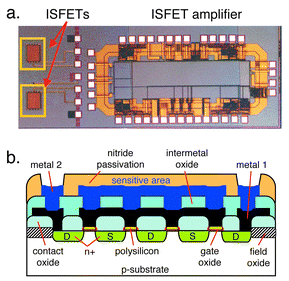 | ||
| Fig. 10 (a) Micrograph of a CMOS chip hosting two integrated ISFETs and an ISFET amplifier. (b) Schematic and cross-section of the ISFET. For details, see text and ref. 131. Reprinted from ref. 131 with permission. | ||
The system includes an ISFET amplifier (source and drain follower) and two interdigitated ISFETs realized in a 1.0 μm, two-metal CMOS process (Atmel-ES2, Atmel, France). The pH measurements have been conducted using a Ag/AgCl reference electrode and yielded a sensitivity of 47 mV per pH unit using silicon oxynitride as the pH-sensitive material.131 To render the fabrication CMOS-compatible, the sensitive oxynitride sits on top of an electrically floating multi-conductor gate structure including the two metal layers and the gate polysilicon, all of which are electrically connected (Fig. 10b). This way, the pH-dependent electrical charge at the surface of the oxynitride in contact with the solution directly affects the silicon surface source–drain current (Fig. 10b).131
4.4.3.1 Chemoresistors. Chemoresistors rely on changes in the electric conductivity of a film or bulk material upon interaction with an analyte. Chemoresistors are usually arranged in a metal electrode 1/sensitive layer/metal electrode 2 configuration.20,21,24 The resistivity/conductance measurement is done either via a Wheatstone bridge arrangement or by recording the current at an applied voltage in a DC (direct current) mode or in a low-amplitude, low-frequency AC (alternating current) mode to avoid electrode polarization. The contact resistance should be much lower than the sample resistance and be minimized, so that the bulk contribution dominates the measured overall conductance.
There is two major classes of chemoresistors: (1) high-temperature chemoresistors (200–600 °C) with semiconductor metal oxide coatings and (2) low-temperature chemoresistors (room temperature) with polymeric and organic sensitive coatings. We will focus on the technologically more challenging high-temperature sensors and only briefly mention the second type with the applications.
The sensitive materials used with high-temperature chemoresistors include wide-bandgap semiconducting metal oxides such as tin oxide, gallium oxide, indium oxide, or zinc oxide, all of which can only be operated as sensing materials at high temperature (>200 °C). In general, gaseous electron donors (hydrogen) or acceptors (nitrogen oxide) adsorb on the metal oxides and form surface states, which, at high temperature, can exchange electrons with the semiconductor. An acceptor molecule will extract electrons from the semiconductor metal oxide and thus decrease its conductivity. The opposite holds true for an electron–donating surface state. The reaction between gases and oxide surface depends on the sensor temperature, the gas involved, and the sensor material.20,140–144
Semiconductor metal oxide sensors usually are not very selective, but respond to almost any analyte (carbon monoxide, nitrogen oxide, hydrogen, hydrocarbons). One method to modify the selectivity pattern includes surface doping of the metal oxide with catalytic metals such as platinum, palladium, gold, and iridium.20,21,140–144
The device requirements for a high-temperature chemoresistor include a thermally well-isolated stage such as a membrane, which allows for keeping the sensing materials at a high temperature without heating the bulk chip (protection of electronic components), an integrated heater, and a temperature sensor (Fig. 11).145,146
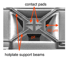 | ||
| Fig. 11 Scanning electron micrograph of a microhotplate. The suspended plate exhibits a polysilicon heater, an aluminum plane for homogenous heat distribution and noble metal-coated aluminum electrodes for measuring the resistance of a semiconductor metal oxide. Reprinted from refs. 145 and 146 with permission. | ||
Fig. 11 shows a front-side-etched microhotplate on a CMOS substrate.145,146 The microhotplate components include a polysilicon resistive heater, an aluminum metal plate for heat distribution and temperature measurement and four noble metal-coated aluminum or tungsten contacts for electrical connection to the sensing film.145,146 Tin dioxide is then deposited on top of the metal electrodes.
Since microhotplates have a very low thermal mass, they allow for applying temperature-programmed operation modes, which enhance the gas detection capability.147,148
The fabrication of hotplates on CMOS-substrates is described in refs. 145, 146, 149 and 150. Complete processing sequences are detailed in refs. 150 and 151. First results with hotplates and circuitry on a single CMOS-chip have been presented recently.152,153 Multi-chip solutions have been proposed in refs. 154 and 155. Reliability tests with CMOS hotplates have been conducted.156 CMOS-hotplates realized on SOI (silicon on insulator) and SIMOX (separation by implantation of oxygen) substrates are presented in refs. 157 and 158.
Typical microhotplate applications include the detection of inorganic gases such as hydrogen,145,146,150 oxygen,145,146 nitrogen oxide,147,159 carbon monoxide,145–148,155,159 and a variety of organic volatiles145,146,150,159–161 using predominantly tin oxide as sensitive layer.
Several classes of predominantly organic materials are used for application with chemoresistors at room temperature (electrode spacing typically 5 to 100 μm, applied voltage 1–5 V). Conducting polymers such as polypyrroles, polyaniline and polythiophene are used to monitor a variety of polar organic volatiles like ethanol, methanol, and components of aromas.162–165 Conducting carbon black can be dispersed in non-conducting polymers so that if the polymer absorbs vapor molecules and swells, the particles are, on average, further apart and the conductivity of the film is reduced (conductivity by particle-to-particle charge percolation).166 Applications also include organic solvents such as hydrocarbons, chlorinated compounds, and alcohols.166–170
CMOS-based monolithic sensor systems coated with carbon black/polymer blends are detailed in,169,170 two-chip solutions with a CMOS circuitry chip and a separate sensor chip based on conducting polymers can be found in refs. 164 and 165. A CMOS-compatible monolithic conductivity sensor for liquid phase (Pt electrodes) was presented in ref. 171.
4.4.3.2 Chemocapacitors. Chemocapacitors (dielectrometers) rely on changes in the dielectric properties of a sensing material upon analyte exposure. Interdigitated electrode structures are predominantly used.172,173 The capacitances usually are measured at an AC frequency of a few kHz up to 500 kHz.
The interdigitated capacitors described here exhibit an electrode width and spacing of 1.6 μm. The total footprint of a capacitor is 800 × 800 μm2. Since the nominal capacitance of such a microstructure is on the order of 1 pF and the expected capacitance changes (sensor signals) in the range of some attoFarads, an integrated solution with on-chip circuitry is required. There is no possibility to transfer such minute analog signals via bond wires and cables to desktop instruments. The integrated solution includes two capacitors, a polymer-coated sensing capacitor and a silicon nitride-passivated reference capacitor in a switched-capacitor scheme (Fig. 12). The sensor response is read out as a differential signal between the polymer-coated sensing and a passivated reference capacitor. A digital output signal is then generated by comparing the minute loading currents of both capacitors using a fully differential second-order Sigma–Delta-modulator circuitry.174,175 A counter to decimate the output bit stream is co-integrated on-chip. A schematic of a capacitive chemical sensor microsystem is shown in Fig. 12.
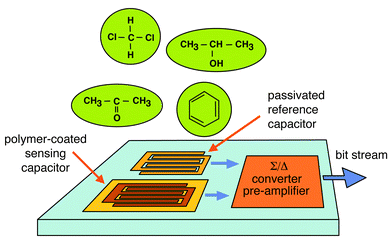 | ||
| Fig. 12 Schematic of a capacitive chemical sensor microsystem including a polymer-coated sensing capacitor and a Si-nitride-protected reference capacitor. The on-chip circuitry includes a ΣΔ-converter. | ||
Two effects change the capacitance of a polymeric sensitive layer upon absorption of an analyte: (i) swelling and (ii) change of the dielectric constant due to incorporation of the analyte molecules into the polymer matrix.46,174,176 The capacitance change for a polymer layer with a thickness of approximately half the periodicity of the electrodes is determined by the ratio of the dielectric constants of analyte and polymer. If the dielectric constant of the polymer is lower than that of the analyte, the capacitance will be increased. Conversely, if the polymer dielectric constant is larger, the capacitance will be decreased (see Fig. 15 later). These effects have been further discussed and supported by simulations in ref. 176.
For conducting measurements at defined temperatures, sensor and reference capacitors can be placed on thermally isolated membrane structures.175
The fabrication of capacitors integrated with CMOS circuitry components is described in refs. 46, 173–178.
Typical applications include humidity sensing with polyimide films,172,173,177–179 since water has a high dielectric constant of 78.5 (liquid state) at 298 K leading to large capacitance changes. CMOS-based integrated capacitive humidity sensors are commercially available from, e.g., Sensirion AG, Switzerland.180 More recent applications also include the detection of organic volatiles in the gas phase using polymeric layers.46,174–176
4.5 Monolithic integration of different transducers
Another significant advantage of CMOS-based chemical sensors is the possibility to integrate several different transducers along with all the driving circuitry on a single chip. Additional components that can be integrated include signal conditioning circuitry (amplifiers, references), multiplexers to reduce the number of output pins, analog/digital and digital/analog converters, chip memory (calibration values) or other smart features, an intra-chip communication or bus system and a serial interface to communicate with off-chip microcontrollers or instruments. In the following we will present two prototype monolithic CMOS multisensor systems, (1) a multiparameter biochemical sensor181 and (2) smart gas sensor microsystem.182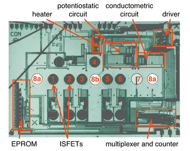 | ||
| Fig. 13 Micrograph of the CMOS multi-parameter biochemical sensor chip, which includes 6 ISFETS (1–6), one conductometric sensor (8a,b) and an (amperometric) oxygen sensor (7). The on-chip circuitry includes an EPROM, a multiplexer and counter, a driver unit, a conductometric and potentiostatic circuit and a heater. Reprinted with permission from ref. 181. | ||
The six ISFETs allow for direct contact of the electrolyte with the gate oxide. The gate oxide itself is pH-sensitive (see ISFET section), or the ISFET can be used as a ‘Severinghaus’-type pH-FET to measure dissolved carbon dioxide (detection of carbon dioxide via dissolution in water, formation of ‘carbonic acid’ and monitoring of the pH change). The gate oxide can also be covered with different ion-selective membranes to achieve sensitivity to a range of target ions such as potassium. All six ISFETs or only a subset can be used. The idea is to make a standard chip to reduce manufacturing costs and then modify the chip with selective coatings according to user needs.
The integrated amperometric sensor can be used as a Clark-type oxygen sensor, which is based on a two-step-reduction of gaseous oxygen in aqueous solution via hydrogen peroxide to hydroxyl ions.
The conductometric sensor consists of two parallel sensors (8a), which share one common electrode (8b). A sinusoidal AC potential is applied to the electrodes, and the current, which depends on the solution composition (concentration of charged particles or ions) is recorded. The eight sensors can continuously monitor ions, dissolved gases and biomolecules via enzymatic reactions that produce charged particles.
The full system is produced in a 1.2 μm single-metal, single-poly CMOS process and the chip size is 4.11 × 6.25 mm.181 The chip is operated at 5 V and hosts all driving circuitry for the sensors such as ISFET buffer amplifiers, a potentiostatic setup for the amperometric sensor and the circuitry necessary to perform a four-point conductometric measurement on chip. In addition the chip exhibits a temperature control unit to keep the system temperature at an adjusted value (physiological conditions). This temperature control unit includes a temperature sensor (parasitic vertical p–n–p bipolar transistor) and a NMOS transistor heater. A single-bit EPROM (electrically programmable read-only memory) was implemented on chip to make sure the chip is only used once and then is disposed, which is a crucial feature in medical applications. Additional on-chip electronics include units to control the chip (multiplexer, demultiplexer, 4-bit Gray counter and decoder) and units to provide the biasing and the communication to off-chip instrumentation. Due to the high level of on-chip integration only 5 external connections are needed: two for power supply, two for bi-directional communication and one for a clock signal.
First tests including amperometric oxygen measurements, the assessment of potassium concentrations with ISFETs, and conductometric measurements with a buffer solution have been performed.181
The capacitive sensor as previously described in section 4.4.3.2 is integrated with a fully differential second-order Sigma-Delta-modulator circuitry and a counter to decimate the output bit stream.185
The micromachined cantilever, the operation principle of which has also been already described in section 4.1.2, is 150 μm long and consists of silicon as well as vapor-deposited and thermal oxide. The cantilever acts as the frequency-determining element in a feedback oscillation circuit, which is entirely integrated on the chip with a counter. For more details on the electronics, see refs. 43 and 185.
The third transducer is a thermoelectric calorimeter based on the Seebeck effect with 256 polysilicon/aluminum thermocouples connected in series (500 μm by 500 μm dielectric membranes). Details have been described in section 4.2.2. The thermovoltage is translated into a digital signal on chip using a Sigma–Delta analog/digital converter and a decimation filter.
The overall system chip additionally includes a temperature sensor since volatile absorption in polymers is strongly temperature-dependent. The temperature sensor relies on the linear temperature dependence of a bipolar transistor available in the CMOS process. The voltage is converted to a digital signal using a Sigma–Delta converter. After calibration, the temperature sensor exhibits an accuracy of 0.1 °C at operation temperatures between −40 and 80 °C.
A micrograph of the microsystem chip is displayed in Fig. 14. The overall chip size is 7 × 7 mm. The chip exhibits all the sensor-specific driving circuitry and signal-conditioning circuitry, which has been described in the context of the different transducers. The analog/digital conversion is done on chip, which allows for achieving a favorable signal-to-noise ratio, since noisy connections are avoided and a robust digital signal is generated on chip and then transmitted to an off-chip data port via an I2C serial interface.186 The I2C bus interface offers the additional advantage of having only very few signal lines (essentially two) for bi-directional communication and also allows for operating multiple chips on the same bus system. An on-chip digital controller manages the sensor timing and the chip power budget. The sensors are located in the center of a metal frame, which is used to apply a flip-chip packaging technique.187
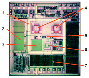 | ||
| Fig. 14 Micrograph of the gas microsensor system chip (size: 7 × 7 mm). The different components include: (1) flip-chip frame, (2) reference capacitor, (3) sensing capacitor, (4) calorimetric sensor and reference, (5) temperature sensor, (6) mass-sensitive resonant cantilever, and (7) digital interface. Reprinted with permission from ref. 182. | ||
Fig. 15 displays simultaneously recorded sensor signals of all three transducers upon exposure to 1200 and 3000 ppm (parts per million) of ethanol, and 1000 and 3000 ppm of toluene at 30 °C.181,185 The sensors were alternately exposed to analyte gas and pure carrier gas. The polymeric coating consisted of poly(etherurethane), PEUT46 at a thickness of approximately 4 μm.
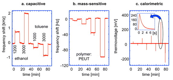 | ||
| Fig. 15 Sensor signals simultaneously recorded from all three polymer-coated transducers upon exposure to 1200 and 3000 ppm of ethanol and 1000 and 3000 ppm of toluene at 301 K: (a) frequency shifts (Sigma–Delta converter output) of the capacitor, (b) frequency shifts of the resonating cantilever, and (c) thermovoltage transients of the calorimetric sensor. The close-up shows the development of the calorimetric transient within 6 s. Reprinted with permission from ref. 182. | ||
Fig. 15a shows the measured frequency signals (Sigma–Delta converter output) of the capacitor. Ethanol exhibiting a dielectric constant of 24.5, which is larger than that of PEUT (2.9), causes a capacitance increase and hence positive frequency shifts, toluene with a dielectric constant of 2.4 causes a capacitance decrease and negative frequency shifts. Fig. 15b displays the cantilever response. The resonance frequency decreases with increasing oscillating mass as a consequence of volatile absorption. Ethanol shows rather low signals as compared to toluene due to its lower molecular mass and due to its lower enrichment (partitioning) in the polymeric phase.
The calorimetric results in Fig. 15c represent a superposition of already discussed partitioning and heat budget change due to analyte ab/desorption. The absorbing analyte liberates heat (heat of condensation) causing a positive transient signal (positive peak), whereas the desorbing analyte abstracts vaporization heat from the environment generating a negative transient signal (negative peak upon purging, see Fig. 15c). The close-up in the upper left corner shows the time-resolved response upon 3000 ppm of toluene within the first 6 s.
The signals of all three transducers linearly correlate with analyte concentration at low concentrations (less than 3% of saturation vapour pressure at the operating temperature). To further improve analyte identification/quantification, an array of microsystem chips coated with different polymers can be used. The monolithic CMOS gas microsystem is targeted at identifying organic solvents in transport containers or providing workplace safety in, e.g., chemical industry. It will form part of a handheld or credit card size detection unit.
5 Outlook
The field of CMOS-integrated chemical sensors is currently expanding as can be seen from the growing number of publications in the last years. As can be concluded from the article, the research and development thrusts go in the direction of integrating more and more electronic functions on the sensor chip such as adaptive circuits for signal evaluation and discrimination,188,189 or telemetry units for wireless communication. Telemetry functions will encompass, e.g., communication from implanted chips (glucose sensors) through the skin in medical applications190 or the transmission of remote and distributed chemical sensor responses to a central terminal in environmental and building control scenarios by using radio frequencies191–193 or other standards like Bluetooth™.194Another extensively belabored field of research will target the combination of CMOS chips with biomaterial such as living cells or neurons. Portable, cell-based biosensor systems with CMOS chips have been reported on by Kovacs and coworkers.195,196 The interfacing of neurons or nerve ends with CMOS circuitry to develop neural probes,197–199 neuromuscular microstimulators,200 or neural prostheses is at an early stage but will gain momentum and will most probably also include monitoring of chemical parameters (ionic signals have to be translated into electronic signals). Sensor arrays for DNA-analysis based on CMOS-assisted electronic detection rather than optical detection may also constitute an interesting application for CMOS technology.201,202
In summary, CMOS and CMOS-MEMS technology and processes offer a great deal of readily available electronic circuits provided by the huge development efforts of the IC-industry, only a small fraction of which has been used for chemical sensors so far. It has to be kept in mind, however, that CMOS sensor development is expensive (mask and processing costs) and only pays off, if either millions or at least hundreds of thousands of pieces are sold, or if the devices provide unique functionality, which then makes up for the costly development. The ‘killer-applications’ involving large numbers of chemical sensors have not emerged yet. They may be in the field of automotive applications, domestic gas alarms, HVAC (humidity, ventilation, air conditioning) units, or in the field of disposable medical devices (e.g., DNA or blood tests).
6 Acknowledgements
The authors are greatly indebted to current and former staff of the Physical Electronics Laboratory at ETH Zurich involved in the chemical microsensor development, notably Christoph Hagleitner, Dirk Lange, and Oliver Brand.7 References
- A. Van den Berg, P. D. van der Waal, B. B. van der Schoot and N. F. de Rooij, Sens. Mater., 1994, 6, 23–43 Search PubMed.
- G. Müller, P. P. Deimel, W. Hellmich and C. Wagner, Thin Solid Films, 1997, 296, 157–163 CrossRef.
- G. T. A. Kovacs, Micromachined Transducers, MCB McGraw-Hill, New York, 1998 Search PubMed.
- M. Elwenspoek and H. Hansen, Silicon Micromachining, Cambridge University Press, Cambridge, 1998 Search PubMed.
- M. Madou, Fundamentals of Microfabrication, CRC Press, Boca Raton, FL, 1997 Search PubMed.
- J. W. Gardner, V. K. Varadan and O. O. Awadelkin, Microsensor, MEMS and Smart Devices, Wiley, New York, 2001 Search PubMed.
- M. Gad-el-Hak, The MEMS Handbook, CRC Press, Boca Raton, 2002 Search PubMed.
- S. Middelhoek and S. A. Audet, Silicon Sensors, Academic Press Inc., London, 1989 Search PubMed; S. Middelhoek, Sens. Actuators, A, 1994, 41–42, 1–8 Search PubMed.
- Silicon Sensors and Circuits: On–chip Compatibility, ed. R. F. Wolffenbuttel, Chapman and Hall, London, 1996 Search PubMed.
- J. L. Rodriguez, R. C. Hughes, W. T. Corbett and P. J. McWhorter, Technical Digest IEEE International Electron Devices Meeting New York, NY, USA, 1992, pp. 521–524 Search PubMed.
- M. J. Vellekoop, G. W. Lubking, P. M. Sarro and A. Venema, Sens. Actuators, A, 1994, 44, 249–263 Search PubMed.
- H. Baltes and O. Brand, IEEE AES Systems Magazine, 1999, 14, 29–34 Search PubMed; H. Baltes and O. Brand, Proc. SPIE-Int. Soc. Opt. Eng., 1999, 3673, 2–10 Search PubMed.
- H. Baltes and O. Brand, Sens. Actuators, A, 2001, 92, 1–9 Search PubMed.
- Semiconductor Sensors, ed. S. M. Sze, Wiley, New York, 1994 Search PubMed.
- S. M. Sze, Physics of Semiconductor Devices, Wiley, New York, 1981 Search PubMed.
- C. Y. Chang and S. M. Sze, VLSI Technology, McGraw Hill, New York, 1996 Search PubMed.
- W. Menz, J. Mohr and O. Paul, Microsystem Technology, Wiley-VCH, Weinheim, 2001 Search PubMed.
- O. Brand and H. Baltes, in Sensors Update, ed. H. Baltes, W. Göpel and H. Hesse, VCH, Weinheim, Germany, vol. 4, 1999 Search PubMed.
- Sensors: A Comprehensive Survey, Chemical and Biochemical Sensors, ed. W. Göpel, J. Hesse and J. N. Zemel, VCH-Verlagsgesellschaft, Weinheim, Germany, 1991, vol. 2–3; Sensors Updates 1–9, ed. H. Baltes, W. Göpel and J. Hesse, VCH-Wiley, Weinheim, Germany Search PubMed.
- J. Janata, Principles of Chemical Sensors, Plenum, New York, 1989 Search PubMed.
- Solid State Chemical Sensors, ed. J. Janata and R. J. Huber, Academic Press, San Diego, 1985 Search PubMed.
- B. R. Eggins, Chemical Sensors and Biosensors, Wiley, Chichester, 2002 Search PubMed.
- Handbook of Biosensors and Electronic Noses, ed. E. Kress-Rodgers, CRC Press Inc., Boca Raton, FL, 1997 Search PubMed.
- M. J. Madou and S. R. Morrison, Chemical Sensing with Solid State Devices, Academic Press, Boston, 1989 Search PubMed.
- J. W. Gardner, Microsensors, Wiley, Chichester, 1994 Search PubMed.
- J. W. Grate and G. C. Frye, in Sensors Update; ed. H. Baltes, W. Göpel and J. Hesse, VCH, Weinheim, Germany, 1996, vol. 2, pp. 37–83 Search PubMed.
- J. W. Grate, S. J. Martin and R. M. White, Anal. Chem., 1993, 65, 940A–948A and 987A–996A.
- D. S. Ballantine, R. M. White, S. J. Martin, A. J. Ricco, G. C. Frye, E. T. Zellers and H. Wohltjen, Acoustic Wave Sensors: Theory, Design, and Physico–Chemical Applications, Academic Press, San Diego, 1997 Search PubMed.
- S. W. Wenzel and R. M. White, IEEE Trans. Electron Devices, 1988, 35, 735–743 CrossRef.
- S. W. Wenzel and R. M. White, Appl. Phys. Lett., 1989, 54, 1976 CrossRef.
- S. W. Wenzel and R. M. White, Sens. Actuators, A, 1990, 21–23, 700–703 Search PubMed.
- M. J. Vellekoop, G. W. Lubking, P. M. Sarro and A. Venema, Sens. Actuators, A, 1994, 249–263 Search PubMed.
- M. J. Vellekop, A. J. Van Rhijn, G. W. Lubking and A. Venema, Sens. Actuators, A, 1991, 25–27, 699–703 Search PubMed.
- S. J. Martin, M. A. Butler, J. J. Spates, M. A. Mitchell and W. K. Schubert, J. Appl. Phys., 1998, 83, 4589–4601 CrossRef CAS.
- W. K. Schubert, D. R. Adkins, M. A. Butler, S. J. Martin, M. A. Mitchell, R. Kottenstette and K. O. Wessendorf, Proceedings of the ECS Meeting Honolulu, Hawaii, 1999, vol. 99–23, pp. 332–335 Search PubMed.
- B. A. Martin, S. W. Wenzel and R. M. White, Sens. Actuators, A, 1990, 21–23, 704–708 Search PubMed.
- A. W. Wang, R. Kiwan, R. M. White and R. L. Ceriani, Sens. Actuators, B, 1998, 49, 13–21 CrossRef.
- J. K. Gimzewski, C. Gerber, E. Meyer and E. E. Schlittler, Chem. Phys. Lett., 1994, 217, 589–594 CrossRef CAS.
- J. Fritz, M. K. Baller, H. P. Lang, H. Rothuizen, P. Vettiger, E. Meyer H. J. Güntherodt C. Gerber and J. K. Gimzewski, Science, 2000, 288, 316–318 CrossRef CAS.
- H. P. Lang, M. K. Baller, R. Berger, C. Gerber, J. K. Gimzewski, F. Battiston, P. Fornaro, J. P. Ramseyer, E. Meyer and H. J. Güntherodt, Anal. Chim. Acta, 1999, 393, 59–65 CrossRef CAS.
- A. Boisen, J. Thaysen, H. Jesenius and O. Hansen, Ultramicroscopy, 2000, 82, 11–16 CrossRef CAS.
- H. Jesenius, J. Thaysen, A. A. Rasmussen, L. H. Veje, O. Hansen and A. Boisen, Appl. Phys. Lett., 2000, 76, 2615–2617 CrossRef.
- D. Lange, C. Hagleitner, A. Hierlemann, O. Brand and H. Baltes, Anal. Chem., 2002, 74, 3084–3095 CrossRef CAS.
- D. Lange, C. Hagleitner, O. Brand and H. Baltes, Proceedings of Transducers ‘99, Sendai, Japan, 1999, pp. 1020–1023 Search PubMed.
- H. Baltes, D. Lange and A. Koll, IEEE Spectrum, 1998, 9, 35–38 CrossRef.
- A. Hierlemann, D. Lange, C. Hagleitner, N. Kerness, A. Koll, O. Brand and H. Baltes, Sens. Actuators, B, 2000, 70, 2–11 CrossRef.
- S. S. Lee and R. M. White, Sens. Actuators, A, 1996, 52, 41–45 Search PubMed.
- Y. Ma, A. M. Robinson, R. P. W. Lawson, W. Allegretto and T. Zhou, Can. J. Phys., 1998, 76, 747–758 CrossRef CAS.
- D. Lange, C. HagleitnerC. Herzog, O. Brand and H. Baltes, Proceedings of IEEE MEMS, 2002, Las Vegas, USA, 2002, pp. 304–307 Search PubMed.
- C. Hagleitner, D. Lange, O. Brand, A. Hierlemann and H. Baltes, Proceedings of IEEE ISSCC 2001, San Francisco, USA, 2001, pp. 246–247 Search PubMed.
- T. Thundat, G. Y. Chen, R. J. Warmack, D. P. Allison and E. A. Wachter, Anal. Chem., 1995, 67, 519–521 CrossRef.
- H. P. Lang, R. Berger, F. Battiston, J. P. Ramseyer, E. Meyer, C. Andreoli, J. Brugger, P. Vettiger, M. Despont, T. Mezzacasa, L. Scandella, H. J. Güntherodt, C. Gerber and J. K. Gimzewski, Appl. Phys. A: Solids Surf., 1998, 66, 161–164 Search PubMed.
- M. Maute, S. Raible, F. E. Prins, D. P. Kern, H. Ulmer, U. Weimar and W. Göpel, Sens. Actuators, B, 1999, 58, 505–511 CrossRef.
- F. M. Battiston, J. P. Ramseyer, H. P. Lang, M. K. Baller, C. Gerber, J. K. Gimzewski, E. Meyer and H. J. Güntherodt, Sens. Actuators, B, 2001, 77, 122–131 CrossRef.
- B. H. Kim, F. E. Prins, D. P. Kern, S. Raible and U. Weimar, Sens. Actuators, B, 2001, 78, 12–18 CrossRef.
- S. Precesky, M. Parameswaran, A. Rawics, R. F. B. Turner and U. Reichl, Can. J. Phys., 1992, 70, 1178–1183.
- G. C. M. Meijer and A. W. van Herwaarden, Thermal Sensors, Institute of Physics Publishing, Bristol, UK, 1994 Search PubMed.
- A. R. Baker, Combustible gas-detecting, electrically heatable element, UK Pat. 892530, 1962 Search PubMed.
- R. P. Manginell, J. H. Smith, A. J. Ricco, D. J. Moreno, R. C. Hughes, R. J. Huber and S. D. Senturia, Technical Digest Solid State Sensor and Actuator Workshop Hilton Head Island, SC, USA, 1996, pp. 23–27 Search PubMed.
- R. P. Manginell, J. H. Smith and A. J. Ricco, Proceedings of the 4th Annual Symposium on Smart Structures and Materials SPIE, 1997, pp. 273–284 Search PubMed.
- M. Zanini, J. H. Visser, L. Rimai, R. E. Soltis, A. Kovalchuk, D. W. Hoffman, E. M. Logothetis, U. Bonne, L. Brewer, O. W. Bynum and M. A. Richard, Sens. Actuators, A, 1995, 48, 187–192 Search PubMed.
- R. Aigner, M. Dietl, R. Katterloher and V. Klee, Sens. Actuators, B, 1996, 33, 151–155 CrossRef.
- R. Aigner, F. Auerbach, P. Huber, R. Mueller and G. Scheller, Sens. Actuators, B, 1994, 18–19, 143–147 CrossRef CAS.
- P. Krebs and A. Grisel, Sens. Actuators, B, 1993, 13–14, 155–158 CrossRef CAS.
- M. Gall, Sens. Actuators, B, 1991, 4, 533–538 CrossRef.
- M. Gall, Sens. Actuators, B, 1993, 15–16, 260–264 CrossRef CAS.
- C. H. Mastrangelo, PhD Thesis, UC Berkeley, 1991.
- A. Accorsi, G. Delapierre, C. Vauchier and D. Charlot, Sens. Actuators, B, 1991, 4, 539–543 CrossRef.
- A. W. Van Herwaarden and P. M. Sarro, Sens. Actuators, 1986, 10, 321–346 CrossRef CAS.
- P. M. Sarro, A. W. van Herwaarden and W. van der Vlist, Sens. Actuators, A, 1994, 41–42, 666–671 Search PubMed.
- A. W. Van Herwaarden, P. M. Sarro, J. W. Gardner and P. Bataillard, Sens. Actuators, A, 1994, 43, 24–30 Search PubMed.
- N. Kerness, A. Koll, A. Schaufelbuehl, C. Hagleitner, A. Hierlemann, O. Brand and H. Baltes, Proceedings of the IEEE Workshop on Micro Electro Mechanical Systems MEMS 2000, Myazaki, Japan, 2000, pp. 96–101, ISBN 0-7803-5273-4 Search PubMed.
- A. Koll, A. Schaufelbühl, O. Brand, H. Baltes, C. Menolfi and H. Huang, Proceedings of the IEEE Workshop on Micro Electro Mechanical Systems MEMS 99, Orlando, USA, 1999, pp. 547–551, ISBN 0-7803-5194-0 Search PubMed.
- C. Hagleitner, D. Lange, A. Hierlemann, O. Brand and H. Baltes, IEEE J. Solid-State Circuits, 2002 Search PubMed , in press.
- P. M. Sarro, H. Yashiro, A. M. van Herwaarden and S. Middelhoek, Sens. Actuators, 1988, 14, 191–201 CrossRef CAS.
- J. Lerchner, J. Seidel, G. Wolf and E. Weber, Sens. Actuators, B, 1996, 32, 71–75 CrossRef.
- D. Caspary, M. Schröpfer, J. Lerchner and G. Wolf, Thermochim. Acta, 1999, 337, 19–26 CrossRef CAS.
- J. Lerchner, A. Wolf and G. Wolf, J. Therm. Anal., 1999, 55, 212–223 Search PubMed.
- P. Bataillard, E. Steffgen, S. Haemmerli, A. Manz and H. M. Widmer, Biosens. Bioelectron., 1993, 8, 89–98 CrossRef CAS.
- J. M. Köhler, E. Kessler, G. Steinhage, B. Gründig and K. Cammann, Mikrochim. Acta, 1995, 120, 309–319.
- O. Wolfbeis, G. E. Boisde and G. Gauglitz, in Sensors: A Comprehensive Survey, ed. W. Göpel, J. Hesse and J. N. Zemel, VCH-Verlagsgesellschaft, Weinheim, 1991, vol. 2, pp. 573–646 Search PubMed.
- G. Gauglitz, in Sensors: A Comprehensive Survey, ed. W. Göpel, J. Hesse and J. N. Zemel, VCH-Verlagsgesellschaft, Weinheim, 1996, update vol. 1, pp. 1–49 Search PubMed.
- A. Brecht, G. Gauglitz and W. Göpel, in Sensors: A Comprehensive Survey, ed. H. Baltes, W. Göpel and J. Hesse, VCH-Verlagsgesellschaft, Weinheim, 1998, update vol. 3, pp. 573–646 Search PubMed.
- H. Zappe, in Sensors: A Comprehensive Survey, ed. H. Baltes, W. Göpel and J. Hesse, VCH-Verlagsgesellschaft, Weinheim, 1999, update vol. 5, pp. 1–45 Search PubMed.
- U. E. Spichiger-Keller, Chemical Sensors and Biosensors for Medical and Biological Application, Wiley-VCH, Weinheim, 1998 Search PubMed.
- Optical Fiber Sensors, ed. J. Dakin and B. Culshaw, Artech House, Norwood, MA, 1997, vols. 3 and 4 Search PubMed.
- Chemical and Biochemical Sensing with Optical Fibers and Waveguides, ed. G. E. Boisde and A. Harmer, Artech House, Norwood, MA, 1996 Search PubMed.
- O. S. Wolfbeis, Anal. Chem., 2000, 72, 81R–90R CrossRef CAS.
- M. Simpson, G. Sayler, D. Nivens, S. Ripp, M. Paulus and G. Jellison, Trends Biotechnol., 1998, 16, 332–338 CrossRef CAS.
- M. Simpson, M. Paulus, G. Jellison, G. Sayler, B. Applegate, S. Ripp and D. Nivens, Technical Digest: Solid-State Sensor and Actuator Workshop, Hilton Head, USA, 1998, pp. 354–357 Search PubMed.
- M. Simpson, G. Sayler, D. Nivens, S. Ripp, M. Paulus and G. Jellison, Proc. SPIE-Int. Soc. Opt. Eng., 1998, 3328, 202–212 Search PubMed.
- G. M. Yee, N. I. Maluf, P. A. Hing, M. Albin and G. T. Kovacs, Sens. Actuators, A, 1997, 58, 61–66 Search PubMed.
- G. M. Yee, N. I. Maluf and G. T. Kovacs, Technical Digest Transducers, Sendai, Japan, 1999, pp. 1882–1883 Search PubMed.
- G. De Graaf and R. F. Wolffenbuttel, Sens. Actuators, A, 1998, 67, 115–119 Search PubMed.
- R. F. Wolffenbuttel, in Sensors: A Comprehensive Survey, ed. H. Baltes, J. Hesse and J. Korvink, VCH-Verlagsgesellschaft, Weinheim, 2001, update vol. 9, pp. 69–101 Search PubMed.
- J. H. Correia, G. de Graaf, S. H. Kong, M. Bartek and R. F. Wolffenbuttel, Sens. Actuators, A, 2000, 82, 191–197 Search PubMed.
- M. Lambrechts and W. Sansen, Biosensors: Microelectrochemical Devices, Institute of Physics Publishing, Bristol, 1992 Search PubMed.
- P. Fabry and E. Sieber, in The GRC Handbook of Solid State Electrochemistry, ed. P. J. Gellings and H. J. M. Bouwmeester, CRC Press, Boca Raton, FL, 1997 Search PubMed.
- U. Wollenberger, in Biotechnology and Engineering Reviews, Artech House, Norwood, UK, 1996, vol. 13, pp. 237–266 Search PubMed.
- W. Sansen, D. de Wachter, L. Callewaert, M. Lambrechts and A. Claes, Sens. Actuators, B, 1990, 1, 298–302 CrossRef.
- H. Hinkers, C. Sundermeier, R. Lürick, F. Walfort, K. Cammann and M. Knoll, Sens. Actuators, B, 1995, 26–27, 398–400 CrossRef.
- Z. Huixian, L. Tai Chin, L. Ralf and R. Reinhard, Sens. Actuators, B, 1998, B46, 155–159.
- Z. B. Zhou, Q. H. Wu and C. C. Liu, Sens. Actuators, B, 1994, 21, 101–108 CrossRef.
- M. Wittkampf, G. C. Chemnitius, K. Cammann, M. Rospert and W. Mokwa, Sens. Actuators, B, 1997, 43, 40–44 CrossRef.
- O. C. Chen, S. Wang, L. Chii Wann and L. Yao Chou, Proceedings of 1997 IEEE International Symposium on Circuits and Systems, ISCAS ′97, Hong Kong, (Cat. No. 97CH35987), pp. 2761–2764 Search PubMed.
- L. Chii Wann, J. Chien Yu, O. C. Chen, S. Wang and T. Kao, Proceedings of the 20th Annual International Conference of the IEEE Engineering in Medicine and Biology Society, 1998, vol. 20, (Cat. No. 98CH36286), pp. 1834–1836 Search PubMed.
- J. Wu, J. Suls and W. Sansen, Sens. Actuators, B, 2001, 78, 221–227 CrossRef.
- R. Kakerow, Y. Manoli, W. Mokwa, M. Rospert, H. Meyer, H. Drewer, J. Krause and K. Cammann, Sens. Actuators, A, 1994, A43, 296–301 Search PubMed.
- J. G. Ryan, L. Barry, C. Lyden, J. Alderman, B. Lane, L. Schiffner, J. Boldt and H. Thieme, IEEE International Solid–State Circuits Conference. Digest of Technical Papers, ISSCC, (Cat. No. 95CH35753), 1995, pp. 158–159 Search PubMed.
- P. Bergveld, IEEE Trans. Biomed. Eng., 1970, BME–17, 70–71.
- I. Lundström, S. Shivaraman, C. Svensson and L. Lundkvist, Appl. Phys. Lett., 1975, 26, 55–57 CrossRef CAS.
- I. Lundström, Sens. Actuators, B, 1996, 56, 75–82.
- L. G. Ekedahl, M. Eriksson and I. Lundström, Acc. Chem. Res., 1998, 31, 249–256 CrossRef CAS.
- J. L. Rodriguez, R. C. Hughes, W. T. Corbett and P. J. McWhorter, International Electron Devices Meeting 1992, San Francisco, USA, Technical Digest, (Cat. No. 92CH3211-0), 1992, pp. 19.6.1–19.6.4 Search PubMed.
- R. C. Hughes, D. J. Moreno, M. W. Jenkins and J. L. Rodriguez, Solids–State Sensor and Actuator Workshop, Hilton Head, USA, Technical Digest, 1994, pp. 57–60 Search PubMed.
- A. Srivastava, N. George and J. Cherukuri, Proc. SPIE-Int. Soc. Opt. Eng., 1995, 2642, 121–129 Search PubMed.
- W. M. Siu and R. S. Cobbold, IEEE Trans. Electronic Devices, 1979, ED–26, 1805–1815 Search PubMed.
- J. Janata, Sens. Actuators, 1983, 4, 255–265 CrossRef CAS.
- I. Lauks, Sens. Actuators, 1981, 1, 261–288 CrossRef CAS.
- L. Bousse and P. Bergveld, Sens. Actuators, 1984, 6, 65 CrossRef CAS.
- A. Van den Berg, P. Bergveld, D. N. Reinhoudt and E. J. R. Sudholter, Sens. Actuators, 1985, 8, 129 CrossRef CAS.
- S. Alegret, J. Bartroli, C. Jimenez Jorquera, M. del Valle, C. Dominguez, J. Esteve and J. Bausells, Sens. Actuators, B, 1992, B7, 555–60 CrossRef.
- K. Chang Soo, S. Hwa Il, L. Chae Hyang, S. Byung Ki, International Conference on Solid-State Sensors and Actuators, Transducers ‘97, Chicago, USA, Digest of Technical Papers, (Cat. No. 97TH8267), 1997, pp. 911–914 Search PubMed.
- I. Gracia, C. Cane and E. Lora Tamayo, Sens. Actuators, B, 1995, B24, 206–210 CrossRef CAS.
- R. L. Smith and D. C. Scott, IEEE Trans. Biomed. Eng., 1986, BME–33, 83–90.
- S. Martinoia, L. Lorenzelli, G. Massobrio, B. Margesin and A. Lui, Sens. Mater., 1999, 11, 279–295 Search PubMed.
- P. Hein and P. Egger, Sens. Actuators, B, 1993, B14, 655–656 CrossRef.
- M. Lehmann, W. Baumann, M. Brischwein, H. J. Gahle, I. Freund, R. Ehret, S. Drechsler, H. Palzer, M. Kleintges, U. Sieben and B. Wolf, Biosens. Bioelectron., 2001, 16, 195–203 CrossRef CAS.
- P. Neuzil, Sens. Actuators, B, 1995, B24, 232–235 CrossRef CAS.
- L. Chae-Hyang, S. Hwa-Il, L. Young-Chul, C. Byung-Woog, J. Hoon and S. Byung-Ki, Sens. Actuators, B, 2000, B64, 37–41.
- J. Bausells, J. Carrabina, A. Errachid and A. Merlos, Sens. Actuators, B, 1999, B57, 56–62 CrossRef.
- M. Armgarth and C. Nylander, Appl. Phys. Lett., 1981, 39, 91–92 CrossRef CAS.
- A. Grisel, C. Francis, E. Verney and G. Mondin, Sens. Actuators, 1989, 17, 285–295 CrossRef CAS.
- D. Ewald, A. Van Den Berg and A. Grisel, Sens. Actuators, B, 1990, B1, 335–340 CrossRef CAS.
- D. N. Reinhoudt, J. F. J. Engbersen, Z. Brzózka, H. H. van den Vlekkert, G. W. N. Honig, H. A. J. Holterman and U. H. Verkerk, Anal. Chem., 1994, 66, 3618 CrossRef CAS.
- P. D. Van der Wal, E. J. R. Sudholter and D. N. Reinhoudt, Anal. Chim. Acta, 1991, 245, 159 CrossRef CAS.
- J. A. J. Brunink, J. R. Haak, J. G. Bomer, D. N. Reinhoudt, M. A. McKervey and S. J. Harris, Anal. Chim. Acta, 1991, 254, 75 CrossRef CAS.
- Z. Brzózka, P. L. H. M. Cobben, D. N. Reinhoudt, J. J. H. Edema, J. Buter and R. M. Kellogg, Anal. Chim. Acta, 1993, 273, 139 CrossRef CAS.
- B. Palan, F. V. Santos, J. M. Karam, B. Courtois and M. Husak, Sens. Actuators, B, 1999, B57, 63–68 CrossRef.
- W. Göpel and G. Reinhardt, in Sensors, ed. H. Baltes, W. Göpel, and J. Hesse, VCH, Weinheim, 1996, update vol. 1, pp. 49–120 Search PubMed.
- N. Barsan and U. Weimar, J. Electroceram., 2001, 7(3), 143–167 CrossRef CAS.
- I. Simon, N. Barsan, M. Bauer and U. Weimar, Sens. Actuators, B, 2001, 73, 1–26 CrossRef.
- H. Geistlinger, Sens. Actuators, B, 1993, 17, 47–60 CrossRef CAS.
- G. Heiland and D. Kohl, in Chemical Sensor Technology, ed. T. Seiyama, Elsevier, Amsterdam, 1988, vol. 1 Search PubMed.
- J. S. Suehle, R. E. Cavicchi, M. Gaitan and S. Semancik, IEEE Electron Devices Lett., 1993, 14, 118–120 Search PubMed.
- S. Semancik and R. E. Cavicchi, Acc. Chem. Res., 1998, 31, 279–287 CrossRef CAS.
- A. Heilig, N. Barsan, U. Weimar, M. Schweizer–Berberich, J. W. Gardner and W. Göpel, Sens. Actuators, B, 1997, 43, 45–51 CrossRef.
- A. P. Lee and B. J. Reedy, Sens. Actuators, B, 1999, 60, 35–42 CrossRef.
- A. Götz, I. Gracia, J. A. Plaza, C. Cane, P. Roetsch, H. Böttner and K. Seibert, Sens. Actuators, B, 2001, B77, 395–400 CrossRef.
- S. Lie Yi, T. Zhenan, W. Jian, P. C. H. Chan and J. K. O. Sin, Sens. Actuators, B, 1998, B49, 81–87.
- S. Majoo, J. L. Gland, K. D. Wise and J. W. Schwank, Sens. Actuators, B, 1996, 35–36, 312–319 CrossRef.
- D. Barrettino, M. Graf, M. Zimmermann, A. Hierlemann, H. Baltes, S. Hahn, N. Barsan and U. Weimar, Proceedings of IEEE ISCAS 2002, Phoenix, USA, 2002, vol. II, pp. 157–160 Search PubMed.
- M. Y. Afridi, J. S. Suehle, M. E. Zaghloul, D. W. Berning, A. R. Hefner, S. Semancik and R. E. Cavicchi, Proceedings of IEEE ISCAS 2002, Phoenix, USA, 2002, vol. II, pp. 732–735 Search PubMed.
- N. Najafi, K. D. Wise, R. Mechant and J. W. Schwank, Technical Digest. IEEE Solid–State Sensor and Actuator Workshop, Hilton Head, USA, (Cat. No. 92TH0403-X), 1992, pp. 19–22 Search PubMed.
- G. C. Cardinali, L. Dori, M. Fiorini, I. Sayago, G. Fagila, C. Perego, G. Sberveglieri, V. Liberali, F. Maloberti and D. Tonietto, Analog Integrated Circuits and Signal Processing, 1997, 14, 275–296 Search PubMed.
- L. Y. Sheng, C. de Tandt, W. Ranson and R. Vounckx, Microelectron. Reliab., 2001, 41, 307–315 CrossRef.
- F. Udrea, J. W. Gardner, D. Setiadi, J. A. Covington, T. Dogaru, C. C. Lu and W. I. Milne, Sens. Actuators, B, 2001, 78, 180–190 CrossRef.
- J. Werno, R. Kersjes, W. Mokwa and H. Vogt, Sens. Actuators, A, 1994, A42, 578–581 Search PubMed.
- D. Vincenzi, M. A. Butturi, V. Guidi, M. C. Carotta, G. Martinelli, V. Guarnieri, S. Brida, B. Margesin, F. Giacomozzi, M. Zen, G. U. Pignatel, A. A. Vasiliev and A. V. Pisliakov, Sens. Actuators, B, 2001, B77, 95–99 CrossRef.
- L. Ratton, T. Kunt, T. McAvoy, T. Fuja, R. Cavicchi and S. Semancik, Sens. Actuators, B, 1997, B41, 105–120 CrossRef.
- R. E. Cavicchi, S. Semancik, R. M. Walton, B. Panchapakesan, D. L. DeVoe, M. Aquino Class, J. D. Allen and J. S. Suehle, Proc. SPIE-Int. Soc. Opt. Eng., 1999, 3857, 38–49 Search PubMed.
- K. C. Persaud and P. Pelosi, Sensor Arrays Using Conducting Polymers in Sensors and Sensory Systems for an Electronic Nose, ed. J. W. Gardner, P. N. Bartlett, Kluwer, Dordrecht, 1992 Search PubMed.
- P. N. Bartlett and J. W. Gardner, Odor Sensor for an Electronic Nose in Sensors and Sensory Systems for an Electronic Nose, ed. J. W. Gardner, P. N. Bartlett, Kluwer, Dordrecht, 1992 Search PubMed.
- J. V. Hatfield, P. Neaves, P. J. Hicks, K. Persaud and P. Travers, Sens. Actuators, B, 1994, B18–19, 221–228 CrossRef CAS.
- P. Neaves and J. V. Hatfield, Sens. Actuators, B, 1995, B26–27, 223–231 CrossRef.
- M. C. Lonergan, E. J. Severin, B. J. Doleman, S. A. Beaber, R. H. Grubbs and N. S. Lewis, Chem. Mater., 1996, 8, 2298–2312 CrossRef CAS.
- E. J. Severin, B. J. Doleman and N. S. Lewis, Anal. Chem., 2000, 72, 658–668 CrossRef CAS.
- S. V. Patel, M. W. Jenkins, R. C. Hughes, W. G. Yelton and A. J. Ricco, Anal. Chem., 2000, 72, 1532–1542 CrossRef CAS.
- J. A. Dickson and R. M. Goodman, Proceedings of the IEEE International Symposium on Circuits and Systems, Geneva, Switzerland, 2000, (IEEE CAt. No. 00CH36353), 2000, vol. 4, pp. 341–344 Search PubMed.
- J. A. Dickson, M. S. Freund, N. S. Lewis and R. M. Goodman, Solid-State Sensor and Actuator Workshop 2000, Hilton Head Island, USA, Technical Digest, (TRF Cat. No. 00TRF-0001), 2000, pp. 162–164 Search PubMed.
- N. Kordas, Y. Manoli, W. Mokwa and M. Rospert, Sens. Actuators, A, 1994, A43, 31–37 Search PubMed.
- N. F. Sheppard, D. R. Day, H. L. Lee and S. D. Senturia, Sens. Actuators, 1982, 2, 263–274 CrossRef.
- S. D. Senturia, Technical Digest Transducers 1985, pp. 198–201 Search PubMed.
- C. Cornila, A. Hierlemann, R. Lenggenhager, P. Malcovati, H. Baltes, G. Noetzel, U. Weimar and W. Göpel, Sens. Actuators, B, 1995, 24–25, 357–361 CrossRef.
- C. Hagleitner, A. Koll, R. Vogt, O. Brand and H. Baltes, Technical Digest Transducers, Sendai, Japan, 1999, vol. 2, pp. 1012–1015 Search PubMed.
- F. P. Steiner, A. Hierlemann, C. Cornila, G. Noetzel, M. Bächtold, J. G. Korvink, W. Göpel and H. Baltes, Technical Digest Transducers 1995, vol. 2, pp. 814–817 Search PubMed.
- T. Boltshauser and H. Baltes, Sens. Actuators, A, 1991, 25–27, 509–512 Search PubMed.
- T. Boltshauser, L. Chandran, H. Baltes, F. Bose and D. Steiner, Sens. Actuators, B, 1991, 5, 161–164 CrossRef.
- C. Laville, J. Y. Deletage and C. Pellet, Sens. Actuators, B, 2001, B76, 304–309 CrossRef.
- http://www.sensirion.com .
- E. Lauwers, J. Suls, W. Gumbrecht, D. Maes, G. Gielen and W. Sansen, IEEE J. Solid-State Circuits, 2001, 36, 2030–2038 Search PubMed.
- C. Hagleitner, A. Hierlemann, D. Lange, A. Kummer, N. Kerness, O. Brand and H. Baltes, Nature, 2001, 414, 293–296 CrossRef CAS.
- A. Witvrouw, F. Van Steenkiste, D. Maes, L. Haspeslagh, P. Van Gerwen, P. De Moor, S. Sedky, C. Van Hoof, A. C. de Vries, A. Verbist, A. De Caussemaeker, B. Parmentier and K. Baert, Microsyst. Technol., 2000, 6, 192–199 CrossRef.
- W. Gumbrecht, D. Peters, W. Schelter, W. Erhardt, J. Henke, J. Steil and U. Sykora, Sens. Actuators, B, 1994, B19, 704–708 CrossRef.
- C. Hagleitner, D. Lange, A. Hierlemann, O. Brand and H. Baltes, IEEE J. Solid-State Circuits, 2002 Search PubMed , in press.
- I2C is a communication standard developed by Philips, Eindhoven, The Netherlands.
- A. Koll, S. Kawahito, F. Mayer, C. Hagleitner, D. Scheiwiller, O. Brand and H. Baltes, Proc. SPIE Smart Structures and Materials, 1998, 3328, 223–232 Search PubMed.
- D. M. Wilson and S. P. DeWeerth, Sens. Mater., 1998, 10, 169–83 Search PubMed.
- A. Apsel, T. Stanford and P. Hasler, Proceedings of the 1998 IEEE International Symposium on Circuits and Systems, ISCAS ′98, (Cat. No. 98CH36187), 1998, vol. 3, pp. 107–110 Search PubMed.
- M. C. Shults, R. K. Rhodes, S. J. Updike, B. J. Gilligan and W. N. Reining, IEEE Trans. Biomed. Eng., 1994, 41, 937–942 CrossRef CAS.
- P. Wouters, M. de Cooman, D. Lapadatu and R. Puers, Sens. Actuators, A, 1994, A41, 198–206 Search PubMed.
- B. Puers, P. Wouters and M. De Cooman, Sens. Actuators, A, 1993, 260–267 Search PubMed.
- K. Bult, A. Burstein, D. Chang, M. Dong, M. Fielding, E. Kruglick, J. Ho, F. Lin, T. H. Lin, W. J. Kaiser, R. Mukai, P. Nelson, F. L. Newburg, K. S. J. Pister, G. Pottie, H. Sanchez, O. M. Stafsudd, K. B. Tan, C. M. Ward, G. Yung, S. Xue, H. Marcy and J. Yao, Technical Digest. Solid–State Sensor and Actuator Workshop, Hilton Head, USA, 1996, pp. 205–210 Search PubMed.
- http://www.bluetooth.com/ .
- J. J. Pancrazio, R. P. Bey, Jr, A. Loloee, S. Manne, H. C. Chao, L. L. Howard, W. Milton Gosney, D. A. Borkholder, G. T. A. Kovacs, P. Manos, D. S. Cuttino and D. A. Stenger, Biosens. Bioelectron., 1998, 13, 971–979 CrossRef CAS.
- B. D. DeBusschere and G. T. A. Kovacs, Biosens. Bioelectron., 2001, 16, 543–556 CrossRef CAS.
- K. Najafi and K. D. Wise, Sens. Actuators, A, 1990, 21–23, 589–591 Search PubMed.
- B. Qing, M. D. Gingerich and K. D. Wise, Technical Digest. Solid–State Sensor and Actuator Workshop, Hilton Head, USA, 1998, pp. 15–18 Search PubMed.
- D. T. Kewley, M. D. Hills, D. A. Borkholder, I. E. Opris, N. I. Maluf, C. W. Storment, J. M. Bower and G. T. A. Kovacs, Technical Digest. Solid-State Sensor and Actuator Workshop. Hilton Head, USA, 1996, pp. 266–271 Search PubMed.
- M. Nardin and K. Najafi, 8th International Conference on Solid–State Sensors and Actuators and Eurosensors IX, Stockholm Sweden 1995, Digest of Technical Papers, (IEEE Cat. No. 95TH8173), 1995, pp. 59–62 Search PubMed.
- P. Caillat, D. David, M. Belleville, F. Clerc, C. Massit, F. Revol Cavalier, P. Peltie, T. Livache, G. Bidan, A. Roget and E. Crapez, Sens. Actuators, B, 1999, B61, 154–162 CrossRef.
- R. Thewes, F. Hofmann, A. Frey, B. Holzapfl, M. Schienle, C. Paulus, P. Schindler, G. Eckstein, C. Kassel, M. Stanzel, R. Hintsche, E. Nebling, J. Albers, J. Hassmann, J. Schülein, W. Goemann and W. Gumbrecht, IEEE International Solid–State Circuits Conference, ISSCC, 2002, San Francisco, USA, Digest of Technical Papers, 2002, pp. 350–351 Search PubMed.
| This journal is © The Royal Society of Chemistry 2003 |