ZnO nanowires fabricated by a convenient route
Jun
Zhang
a,
Lingdong
Sun
*a,
Huayong
Pan
b,
Chunsheng
Liao
a and
Chunhua
Yan
*a
aState Key Laboratory of Rare Earth Materials Chemistry and Applications, PKU-HKU Joint Lab in Rare Earth Materials and Bioinorganic Chemistry, Peking University, Beijing, 100871, P. R. China. E-mail: chyan@chem.pku.edu.cn
bElectron Microscopy Laboratory, Peking University, Beijing, 100871, China
First published on 7th January 2002
Abstract
A convenient microemulsion-mediated hydrothermal process was employed to synthesize ZnO nanowires, which exhibited a strong ultraviolet emission and a relatively weak defect emission. X-Ray diffraction, scanning electron microscopy, transmission electron microscopy and fluorescence spectroscopy were used to characterize the as-prepared ZnO nanowires.
Semiconductor nanowires have exhibited strong grain-size-dependent properties in electronics and optoelectronics, and their one-dimensional nanostructures are liable to be integrated in nano-devices, for instance, as nanowire light-emitting devices with extremely low power consumption.1–3 Various methods, such as chemical vapor deposition,4–7 arc discharge,8 laser ablation,9 solution10,11 and a template-based method,12,13 have been employed to prepare the nanowires. However, the production of nanowires by a simple and mild route still remains a major challenge.
Nowadays, growing interest in one-dimensional oxide nanomaterials, especially ZnO nanowires, is being displayed. ZnO, as a wide bandgap (3.37 eV) semiconductor with a large exciton binding energy (60 meV), has been extensively investigated, due to its promising applications in short-wavelength light-emitting, transparent conductor, piezoelectric materials and room temperature ultraviolet (UV) lasing.14 Recently, a few studies on ZnO nanowires prepared by vapor transport,15 anodic alumina membrane templates13,16 and physical vapor deposition approaches17 were reported. However, the preparation methods mentioned above involve complex procedures, sophisticated equipment and rigorous experimental conditions. Therefore, it is necessary to develop a simple synthetic method to prepare ZnO nanowires for promising wide-ranging applications. Microemulsion or reverse micelle methods have been widely used as a special microreactor for confining the growth of nanomaterials. The shape of the microreactor varies significantly with the reaction conditions, especially the temperature.18 Herein, we report a simple, direct and reproducible synthetic method for preparing ZnO nanowires by a microemulsion-mediated hydrothermal process under mild conditions.
The as-prepared ZnO nanowires have been structurally characterized by X-ray diffraction (XRD, Rigaku Dmax 2000, employing Cu-Kα radiation). A typical XRD pattern of the nanowires is shown in Fig. 1. It can be seen that the nanowires display the wurtzite structure (hexagonal phase, space group P63mc, JCPDS card no. 36-1451) with high crystallinity. Compared with the standard diffraction patterns of ZnO, the discrepancy in the relative peak intensities is associated with the fact that nanowires have preferred growth orientations. Moreover, the relative peak intensity of (100) to (002) in the present case is quite different from that reported by Pan et al.,3 implying that ZnO nanowires prepared by various methods may exhibit different preferred growth orientations.
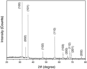 | ||
| Fig. 1 X-Ray diffraction pattern of the ZnO nanowires prepared by the microemulsion-mediated hydrothermal approach. | ||
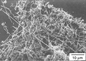
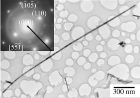
The morphology of the nanowires was examined by scanning electron microscopy (SEM, Amary, FE-1910) and transmission electron microscopy (TEM, Hitachi, H-9000NAR). A typical SEM image, shown in Fig. 2, reveals that the product contains ZnO nanowires with diameters ranging from 30 to 150 nm. The aspect ratio of the nanowires is estimated to be larger than 50. A representative TEM image for a single ZnO nanowire (Fig. 3) shows a nanowire with a diameter of ∼30 nm and a length of up to 3 μm. The selected-area electron diffraction pattern (SAED, inset of Fig. 3) indicates that the ZnO nanowires exhibit a single crystal structure with a preferred growth orientation along the (110) crystal face, based on a calculation of the diffraction dots. The blurry diffraction dots in the inset image might hint at the existence of small crystallites segregated around the nanowires.
The room temperature photoluminescence spectra were performed on a Jobin Yvon-Labram spectrometer with a He–Cd laser focused in about 1 μm as the excitation source at 325 nm. As is shown in Fig. 4, the UV emission at 385 nm was assigned to the recombination of excitonic centers in the nanowires,15 and the emission at 485 nm originated from the radiative recombination of a photogenerated hole with an electron occupying the oxygen vacancy.19
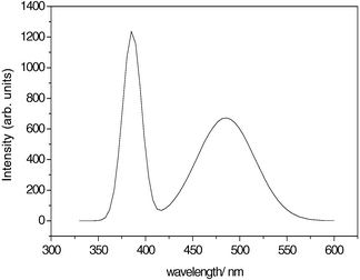 | ||
| Fig. 4 Photoluminescence spectrum of the ZnO nanowires at room temperature. | ||
As for the growth mechanism of the as-made ZnO nanowires, the role of surfactants should be taken into consideration. In the absence of surfactant, ZnO usually crystallizes via a growth-directed process under hydrothermal conditions.20 In the present case, when CTAB and n-hexanol surfactants are both present, the formation of the ZnO nanowires could be induced and achieved via a directed aggregation growth process mediated by the microemulsion droplets, as suggested by Zhang et al.21 At the nucleation stage, the microemulsion droplet may play a role in confining the size and shape of the crystal nucleus.18 At the growth stage, it is considered that the controllable precipitation of Zn(OH)2 inside the droplet microreactor is very beneficial to the growth of the nanowires along preferred orientations. On the other hand, the reaction temperature seems to have certain effects on the growth of nanowires. The detailed mechanism will be further clarified and subsequently addressed elsewhere.
In summary, a microemulsion-mediated hydrothermal approach, which is simple, convenient and mild, has been explored to synthesize ZnO nanowires. A directed aggregation growth process mediated by the reverse micelle droplets is proposed to be responsible for the formation of ZnO nanowires under hydrothermal conditions. It is expected that other oxide nanowires can be made by the same method. Further research in our laboratory is under progress.
Experimental
The nanowire preparation was carried out by using a quaternary microemulsion consisting of 1 g cetyltrimethylammonium bromide (CTAB, AR), 1.2 mL Zn(OH)42− solution formed by adjusting the pH value of zinc acetate solution with NaOH to 14, 3 mL n-hexanol and 10.2 mL n-heptane, as the reaction media. After constant stirring, the microemulsion was transferred into a 25 mL teflon-lined autoclave and heated at 140![[thin space (1/6-em)]](https://www.rsc.org/images/entities/char_2009.gif) °C for 13 h. The white precipitate that formed was collected and washed several times with absolute ethanol and distilled water. Finally, the ZnO nanowires were obtained by centrifugation and drying in vacuum at 60–70°C. The yield of the ZnO nanowires prepared by this method is about 21%.
°C for 13 h. The white precipitate that formed was collected and washed several times with absolute ethanol and distilled water. Finally, the ZnO nanowires were obtained by centrifugation and drying in vacuum at 60–70°C. The yield of the ZnO nanowires prepared by this method is about 21%.
Acknowledgements
This work was supported by NSFC (20001002, 20023005, 29831010), MOST (G19980613), MOE and the Founder Foundation of PKU.References
- K. Hiruma, M. Yazawa, T. Katsuyama, K. Ogawa, K. Haraguchi and M. Koguchi, J. Appl. Phys., 1995, 77, 447 CrossRef CAS.
- J. T. Hu, T. W. Odom and C. M. Lieber, Acc. Chem. Res., 1999, 32, 435 CrossRef CAS.
- Z. W. Pan, Z. R. Dai and Z. L. Wang, Science, 2001, 291, 1947 CrossRef CAS.
- M. Yazawa, M. Koguchi, A. Muto, M. Ozawa and K. Hiruma, Appl. Phys. Lett., 1992, 61, 2051 CrossRef CAS.
- Y. Wu and P. Yang, Chem. Mater., 2000, 12, 605 CrossRef CAS.
- C. C. Chen and C. C. Yeh, Adv. Mater., 2000, 12, 738 CrossRef CAS.
- Z. G. Bai, D. P. Yu, H. Z. Zhang, Y. Ding, X. Z. Gai, Q. L. Hang, G. C. Xiong and S. Q. Feng, Chem. Phys. Lett., 1999, 303, 311 CrossRef CAS.
- Y. C. Choi, W. S. Kim, Y. S. Park, S. M. Lee, D. J. Bae, Y. H. Lee, G.-S. Park, W. B. Choi, N. S. Lee and J. M. Kim, Adv. Mater., 2000, 12, 746 CrossRef CAS.
- (a) X. F. Duan and C. M. Lieber, Adv. Mater., 2000, 12, 298 CrossRef CAS; (b) A. M. Morals and C. M. Lieber, Science, 1998, 279, 208 CrossRef CAS.
- T. J. Trentler, K. M. Hickman, S. C. Goel, A. M. Viano, P. C. Gibbons and W. E. Buhro, Science, 1995, 270, 1791 CrossRef CAS.
- J. D. Holmes, K. P. Johnston, R. C. Doty and B. A. Korgel, Science, 2000, 287, 1471 CrossRef CAS.
- (a) M. H. Huang, A. Choudrey and P. Yang, Chem. Commun., 2000, 12, 1063 RSC; (b) J. Zhu and S. Fan, J. Mater. Res., 1999, 14, 1175 CrossRef CAS.
- Y. Li, G. W. Meng, L. D. Zhang and F. Philipp, Appl. Phys. Lett., 2000, 76, 2011 CrossRef CAS.
- (a) H. Cao, J. Y. Xu, D. Z. Zhang, S.-H. Chang, S. T. Ho, E. W. Seelig, X. Liu and R. P. H. Chang, Phys. Rev. Lett., 2000, 84, 5584 CrossRef CAS; (b) H. Cao, J. Y. Xu, W. Seelig and R. P. H. Chang, Appl. Phys. Lett., 2000, 76, 299; (c) D. M. Bagnall, Y. F. Chen, Z. Zhu, T. Yao, S. Koyama, M. Y. Shen and T. Goto, Appl. Phys. Lett., 1997, 70, 2230 CrossRef CAS; (d) M. H. Huang, S. Mao, H. N. Feick, H. Q. Yan, Y. Y. Wu, H. Kind, E. Weber, R. Russo and P. D. Yang, Science, 2001, 292, 1897 CrossRef CAS.
- M. H. Huang, Y. Y. Wu, H. N. Feick, N. Tran, E. Weber and P. D. Yang, Adv. Mater., 2001, 13, 113 CrossRef CAS.
- Y. Li, G. S. Meng and L. D. Zhang, J. Mater. Res., 2000, 15, 2305 CAS.
- Y. C. Kong, D. P. Yu, B. Zhang, W. Fang and S. Q. Feng, Appl. Phys. Lett., 2001, 78, 407 CrossRef CAS.
- H. Seto, D. Okuhara, Y. Kawabata, T. Takeda, M. Nagao, J. Suzuki, H. Kamikubo and Y. Amemiya, J. Chem. Phys., 2000, 112, 10608 CrossRef CAS.
- K. Vanheusden, W. L. Warren, C. H. Seager, D. R. Tallant, J. A. Voigt and B. E. Gnade, J. Appl. Phys., 1996, 79, 7983 CrossRef CAS.
- C. H. Lu and C. H. Yeh, Ceram. Int., 2000, 26, 351 CrossRef CAS.
- D. B. Zhang, L. M. Qi, J. M. Ma and H. M. Cheng, Chem. Mater., 2001, 13, 2753 CrossRef CAS.
| This journal is © The Royal Society of Chemistry and the Centre National de la Recherche Scientifique 2002 |